Note: Descriptions are shown in the official language in which they were submitted.
CA 02099260 2000-11-06
77312-4
1
A TRI-STATE SWITCHING AMPLIFIER
Introduction
This invention relates generally to power switching
amplifiers and, more particularly, to improved switching
amplifiers which use multiple state power output circuitry,
preferably either ternary, i.e., tri-state, or quaternary,
i.e., quadri-state, power output circuits.
Background of the Invention
Analog amplifiers suffer from several disadvantages
which have given rise to the development of switching, or
discrete state, amplifiers. For a given power output,
especially at relatively high amplitude levels, analog
amplifiers suffer from poor efficiency, primarily because of
the need to bias the acaive elements into linear regions for
amplification without distortion, as in well-known Class A and
Class B analog amplifiers. Since the power dissipated in the
active elements is sub:>t:antial, the resulting amplifier power
efficiency is poor.
Moreover, the low efficiency of analog amplifiers
increases the heat generated therein and results in size and
weight penalties caused by the need to remove the heat
generated. At relatively high power levels, for example, the
amplifiers may require a large passive mechanical heat
exchanger and/or the
W092/12572 zo~~zso
PCT/ L'S91 /0837
- 2 -
use of forced air heat exchangers for heat removal
purposes.
Low efficiency also implies the need for larger
power supplies for a given power output which further
aggravates the efficiency problem because of the heat
losses in the power supplies themselves, thereby
imposing in effect a double penalty. Lower
efficiency also increases costs because the power
handling elements are larger, components having wider
temperature ranges of operation are required, and
heat removal techniques require added cooling
components.
Further, analog amplifiers have an additional
disadvantage when the input signal thereto is taken
from a digital source, such as a CD player, or is
some other serially digitized format signal. In such
cases, an analog amplifier is not fundamentally
compatible with serial digital inputs and requires
intermediate conversion where the digital signal is
first converted to an analog signal either at the
source or in the amplifier, such conversion giving
rise to added complexity and cost to the amplifier,
and often resulting in a degradation of the signal
quality.
Wo 92/m~7~ 2 ~ ~ ~ 2 G ~
PCTII.'S91 /0837 7
- 3 -
Binary switching amplifiers have been used by
those in the art to achieve higher efficiency than
analog amplifiers by the substitution of a switching
control operation for the linear control element in
the output circuitry of the amplifier. Instead of a
linearly biased element, one or more switches are
alternated between on and off states in response to a
digital command that is time modulated by the
amplifier's input analog signal. The time modulated
output signal is then filtered to yield an output
signal that is an amplified replica of the input
signal. Because the active control element comprises
one or more switches which are either in an on or an
off state, the power loss in the active element can
be made relatively low as compared with analog
amplifiers.
The low power losses allow substantial benefits
in terms of the size and cast of the amplifier as
well as in a reduced size and cost of the. associated
power supplies. Cooling can in most cases be handled
by simple thermally conductive paths to the amplifier
package itself, additional cooling components often
not being required.
The fact that the output circuitry is digitally
controlled means that a straightforward interface to
digital signal sources is possible. All the
processing required to create the time modulated
signals can be done at the digital level. For serial
data inputs this can be relatively simple and can
take advantage of many of the new digital signal
processing techniques.
WO 92/ 12572 ? ~ ~ ..
PCT/L S91 /08377
- 4 -
While the use of currently available binary
switching amplifiers provide the above discussed
advantages over the use of analog amplifiers, it is
desirable to improve even further the benefits
derived from the use of switching techniques. For
example, in such binary switching amplifiers, power
dissipation at the output thereof is essentially
constant since one or the.other of the switching
states is always being used. If that power
dissipation can be reduced, the overall power
efficiency of the amplifier can be increased.
Further, for most applications, e.g., in
amplifying music, the average input signal and the
resulting desired average output power are small
compared to the peak power requirements. The
constant power dissipation at the amplifier output,
however, is related only to the peak power capacity.
Thus, a low signal application must always suffer the
power losses associated with the maximum output
capabilities.
Similar losses also appear in the amplifier's
output filter, which is required in all modulated
systems in order to remove the carrier from the
switched output. In a binary amplifier, the carrier
frequency is the same as the sampling and conversion
rate frequency. Since the output switch circuitry is
always connected to a power supply which is providing
power of one polarity or the other into the load,
current is always flowing through the filter elements
even if the net output polarity is zero. Since
realizable filter elements are not purely reactive,
WO 92/125%2 ~ 'S91/083~7
PCT/L
- 5 -
power is dissipated therein, especially in inductive
elements, and the power losses in the filter may be.
as high as those in the switch circuitry itself.
Another problem in using a binary switching
amplifier implementation involves the removal of the
modulation carrier frequency by the output filter.
Because only two output states of opposite polarity
are available, small outputs can only be created by
cancellation of two large signals of opposite
polarity. For a net output of zero, for example, the
actual switched output spends equal times in the two
opposite states. Such a large square wave signal,
when filtered, results in a zero output with some
superimposed ripple. Thus, for the creation of a
very small output, a very large signal must be
supressed by the filter in order to keep the
resulting ripple from entering the load. Such
operation imposes severe design constraints on the
filter both in terms of power handling capacity and
in avoiding any nonlinear filter effects which
generate spurious harmonic energy at the output.
It should be noted that removal of the carrier in
the output is the most difficult when the demanded
output is the smallest, at which time, however, the
ripple effects are the most noticeable, especially in
audio applications. Thus, if the resulting error and
the resulting distortion is measured in proportion to
the output signal, a binary switching amplifier tends
to produce very large percent errors when the signal
being amplified becomes small.
CA 02099260 2000-11-06
77312-4
6
It is desirab:Le to design an amplifier which, while
taking advantage of the benefits obtained when using switching
amplifying techniques as opposed to using analog amplifying
techniques, also overcomes the above problems which arise when
using a binary switching amplifier system.
Brief Summary of the Invention
In accordance with the invention, a switching
amplifier is designed t=o utilize more output switching states
than the two-state swit=ching operation utilized in current
binary switching amplifier systems. In one embodiment of the
invention, a ternary, o:r tri-state, switching operation is
utilized to provide three switching states, namely, positive
power and negative power states, as used in a binary operation,
and a third, or zero, power state. In the third state, a
switching circuit operates as a short circuit to current and
provides effective amp:L:ifier damping. The timing used in
implementing the tri-si.;~te operation is uniquely arranged so
that the critical time phasing thereof prevents major errors
from adversely affecting such operation. The use of ternary
switching automatically provides the desired carrier
suppression and tends i.o minimize the ripple both for small
input signals and for maximum input signals.
The invention may be summarized as an amplifier
system comprising a switching power amplifier including means
responsive to an input signal for providing a tri-state command
signal having discrete amplitudes as a function of time, which
amplitudes represent a positive state, a negative state, or a
zero state; power supp:Ly means capable of supplying a positive
or a negative power oui~put signal; switching means connected to
said power supply mean, and responsive to said tri-state
CA 02099260 2000-11-06
77312-4
6a
command signal for providing a power output signal having
discrete amplitude levels, the time durations and polarities of
which correspond to the states of said tri-state command
signal; filter means responsive to said power output signal for
providing a filtered power output signal to a load, said
filtered power output signal being a substantial replica of
said input signal.
In a further embodiment of the invention, a
quaternary, or four-state, switching operation is utilized in
which, in addition to 1=he three modes of operation in the
ternary switching design, a fourth
WO 92/12572 2 s 9 o z s o ,
PCT/L S91 /083 ~ 7
state is used to reduce distortion effects which may
occur at very small input signal levels below a
selected threshold. In accordance with such
embodiment, the fourth operating state utilizes a
linear amplifier which responds directly to the
sampled input signal so that any distortion at such
. low input levels, which distortion might occur in a
ternary switching operation, are essentially
eliminated and a reproduction and amplification of
very small input signals can be achieved to equal
that achieved by any known analog amplification
system, i.e., there is in effect no ripple signal
present in the linear amplifier output. At the same
time the problems which arise in analog amplifier
systems at higher input signal levels are avoided.
For signals above a selected threshold level, for
example, the advantages of a ternary switching
operation, as discussed above, are available in the
quaternary system.
Description of the Invention
The invention can be described in more detail
with the help of the accompanying drawings wherein
FIG. 1 shows a block diagram of an exemplary
embodiment of a known binary switching amplifier;
FIG. 2, 2A, 2B and 2C show exemplary graphical
representations of signal waveforms present in the
operation of the embodiment of FIG. 1;
FIG. 3 shows a block diagram of an exemplary
embodiment of the invention;
20J9260
WO 92/12572 PCT/l'S91/0837?
_ g _
FIGS. 4, 4A, 4B and 4C show exemplary graphical
representations of signal waveforms present in the
operation of the embodiment of FIG. 3;
FIGS. 5 and 5A show exemplary graphical
representations of ideal and practically realizable
waveforms of a typical output signal obtained in an
embodiment of the invention;
FIGS. 6 and 6A show exemplary graphical
representations of typical command and output signal
waveforms at low input signal levels;
FIG. 7 shows a block diagram of another exemplary
embodiment of the invention:
FIG. 8 shows a chart of the switching states of
the switches for various operating modes of the
embodiment of the invention depicted in FIG. 7; and
FIGS. 9, 9A, 9B and 9C show exemplary graphical
representations of signal waveforms present in the
operation of the embodiment of FIG. 7.
In order to understand the inventibn,
particularly when compared with currently available
binary switching amplifiers, it is helpful to discuss
briefly the structure and operation of known binary
switching systems, with reference to FIGS. 1 and 2.
As shown in FIG. 1, a binary switching amplifier
includes an input sampling circuit l0.for digitally
sampling an analog input signal which is supplied to
an amplitude-to-time converter circuit 11 for
converting the sampled signal into a time modulated
form. A sampled signal is used to prevent any noise
from adversely affecting the subsequent conversion
process. Signals that are varying too quickly may
WO 92/ 12572
PCT/L'S91 /08377
g
also cause a problem which the sampling process
avoids. Alternatively, if the input signal varies
very slowly and has very little noise associated with
it, the sample circuit may in such cases be
eliminated.
The conversion of the sampled signal is performed
using appropriate timing reference and amplitude
reference signals from circuits 12 and 13,
respectively, the overall sample and conversion
process converting an analog input signal into a~
digital signal at the output of converter circuit 11,
the net state-time integral of which is proportional
to the input signal amplitude.
The resulting digital signal, which normally
changes for each successive frame sample of the input
signal, is used via a two-state power switch drive
logic circuit 17 to control the state of selecting
switch circuit 14 that selects either positive~or
negative power from positive and negative power
supplies 15 and 16, respectively. A commonly used
bipolar switch implementation is shown in FIG. 1
which uses relatively simple drive logic and two
power supplies, as would be well known to those in
the art.
The selected power supply output is applied to a
load 19 through an output filter 18. The output
filter averages the output amplitude/time excursions
thereby providing at the load a signal that is a
close replica of the input signal but which has the
~0992UU
WO 92/1257'- PCf/1JS91/08377
- 10 -
added power supplied by the power supplies, i.e., a
power amplified version thereof.
FIGS. 2, 2A, 2B arid 2C show a simplified
presentation of a portion (e. g., five sample frames)
of an input signal at various stages in the binary
switching amplifier circuitry of FIG. 1. For the
example shown, an amplitude-to-time converter uses a
reference ramp signal 26 (FIG. 2A) at each frame
sample to convert the sampled input signal 21 into
variable width pulses 22 (FIG. 2B) which change on
each successful sample for the five sample frames
depicted. The ramp signal can be generated in any
convenient manner, e.g., with an internally generated
waveform signal circuit, the ramp being repeated for
each new sample or by integrating the power~switch
output, as would be well known to those in the art.
When the reference ramp amplitude matches that of the
sampled input signal, the output state is reversed
and the opposite power supply polarity is selected
for the remainder of the sample period. Such
operation results in a switching output signal 23
(FIG. 2B), the net area of which (i.e., the
amplitude/time,product) is proportional to the '
amplitude of the sampled input signal. When such
switching output signal is filtered, the resulting
output signal 24 (FIG. 2C) substantially replicates
the input signal with the presence of ripple from the
filtering process, as shown by filtered output
signal 24.
In order to avoid or reduce the problems which
arise in using such a binary, or two-state, switching
WO 92/12572 ~ ~ ~ ~ ~ ~ ~ PCT/L'S91/08377
- 11 -
operation, the invention uses, in one embodiment
thereof, a tri-state, or ternary, switching operation
as shown with reference to FIG. 3. Circuits 10-13 of
the type shown in FIG. 1 axe used except, as
described in more detail below, the timing and
amplitude reference circuits operate in a different
manner to provide a control signal to a 3-state power
switch drive logic control circuit 25 and a different
switching arrangement 26 is used. In the latter
configuration, a single unipolar power supply 27 is
used with switches 26A, 26B, 26C, 26D to supply a
switched output signal to filter 18 and thence to a
load 19.
In order to provide positive power, switches 26A
and 26D are closed, in order to provide negative
power switches 26B and 26C are closed, and in order
to provide a third, or zero, state, either switches
26A and 26B are closed or switches 26C and 26D are
closed. Such latter operations provide a short
circuit path to any energy that is present on the
load or in the ~ilter.
FIGS. 4, 4A, 4B and 4C show various stages of a
portion of the input signal 20 in a manner similar to
that depicted for the binary switching system in FIG.
2. In the system of FIG. 3, a reference
triangle-shaped signal 30 is used to convert the
sampled input signal 21 into variable width pulses 31
which are changed on each successive sample. The
triangle can be generated either with an internally
generated waveform that is repeated for each new
2099260
WO 92/12572 PCT/l.'S91/08377
- 12 -
sample or by using a suitable integrating technique,
as would be well known to those in the art.
When the magnitude of the reference triangle is
greater than the magnitude of the sampled input, the
output switch is commanded to the zero state. When
the magnitude of the reference triangle is less than
the magnitude of the sampled input, the switch is
commanded to connect the unipolar supply to the load
with the same polarity as the sampled input signal.
This results in a signal whose net area (i.e., the
amplitude-time product) is proportional to the
sampled input. When filtered, the resultant filtered
input signal 32 substantially replicates the input
signal, with greater power, and with the presence of
a ripple, as shown by filtered output signal 32.
It should be noted that the conversion process
described above results in a pulse at the switch
output that is centered within each frame sample and
is roughly sym.~netrical about the midpoint of the
frame since the triangle-shaped reference signal 30
is arranged to be symmetrically disposed within each
time frame. Such pulses differ from the pulses
created in a binary system and avoid producing a
major error as would occur if the conversion were
done using a triangle-shaped reference signal that is
not symmetrical or by using a linear ramp starting at
the beginning of the sample period, as in the binary
case. If such a non-symmetric or ramp reference is
used, the resulting pulse, although having three
states, would not be centered within the sample
frame. If the non-centered signal is then filtered,
VfO 92/ 125 7 2 ~ i~ ~ ~ ~ ~ ~ PC.'T/l,'S91 /08377
- 13 -
a large transient in the the filtered output would
appear whenever the converted input passes through
zero. By using a conversion process that is "frame
centered" such error is removed and distortion of the
filtered output is avoided.
The error effect discussed above can also be
described in terms of modulation theory. The ternary
system as described is ideally a suppressed carrier
system. If the conversion is not frame centered, the
output contains a residual carrier as the signal
approaches zero (i.e., the carrier is not fully
suppressed). When the output inverts, i.e., as the
input crosses zero, both the signal and the residual
carrier are inverted. The step change in carrier
phase at this point injects a signal into the output
filter that is equivalent to a DC step in the input
signal. This causes the output filter to ring and
this error signal is superimposed on the desired
output. By frame centering the pulses, the filter
output ringing effect is substantially reduced or
effectively eliminated. Thus, the output filter
ringing problem is avoided and no carrier error
signal is superimposed on the desired filter output.
The ternary system of the invention also provides
damping of the filter output signal by assuring that
a low source impedance is always present at the input
to the filter. Thus, when switch command pulse
signals are present, as shown by pulses 31, for
example, in FIG. 4B, the source impedance is the low
impedance of the power supply 27 and damping is
provided. When no switch command pulse signal is
2001260
WO 92/ 1257? PCf/ C~S91 /083'7
- 14 -
present, the switches are in the third, or zero,
state, as mentioned above; in which state either
switches 26A and 26B are closed or switches 26C and
26D are closed. In such case the source impedance at
the filter input is effectively zero (the filter
input is effectively shorted) and damping is also
provided. Thus, in accordance with the operation of
the system of the invention, damping of the filter
output signal is always provided, as desired.
The use of a ternary switching operation that can
implement three states and provide damping in the
output eliminates problems inherent in a binary
switching implementation. Moreover, efficiency and
carrier related problems are also essentially
eliminated.
Because of the use of a third state, i.e., a zero
output state, the output circuitry dissipates power
only in proportion to the output signal supplied~by
the converter. Thus, fox small signal inputs, the
power loss is small. For a zero state signal, the
switch is always off so that no losses occur. This
operation allows signficantly smaller switch
circuitry yielding lower cost and higher possible
switching speeds because of the lower distributed
reactances in the switch circuitry itself. The
reduction in power loss reduces heat generation and
allows heat removal using conductive heat sinks to
the amplifier package or in some cases to the wiring
interconnections alone.
WO 92/12572 2 (~ 9 ~ 2 6 ~3 P~/L'S91/08377
- 15 -
Since the speed performance of the switch can now
be improved, the carrier frequency (or the rate of
the conversion process) can be raised. This means a
reduction in sampling rate induced errors because the
frequency of the input response can be raised. At
the same time, the filter can be made smaller because
less reactance is necessary at the higher carrier
frequency to obtain the same carrier rejection.
Even if the carrier frequency is not raised, the
net ripple in the output~signal is much lower than in
the output signal of a binary system because the
carrier has been essentially suppressed before the
signal is even applied to the output filter.
The ripple properties of the suppressed carrier
system are such that the ripple is minimized at the
two extremes of pulse width output, i.e., for
minimum, or near minimum, and maximum, or near
maximum, signals. The minimum pulse width case is
for small signal outputs where the ripple magnitude
is the most damaging to the signal performance.
The maximum ripple for the ternary system occurs
for the signals that are about one half the output
range in either polarity. At this point the signal
waveform from the switch structure to the output
filter appears as a square wave. Its height,
however, is one half that of the binary output for
the same area. Since the voltage excursion has been
reduced by two, the resulting ripple magnitude is
much smaller than that for the binary system at that
level.
wo9Z/i2sr 2099260
PCT/1JS91 /083 % 7
- 16 -
Further, the errors and losses in the filter are
greatly reduced for smaller outputs because the
filter no longer has to handle the large power
dissipation required to achieve peak power. The
filter can now be designed on the basis of average
rather than peak power requirements. As a result, it
can be made smaller and for lower cost for the same
ripple rejection.
The achievement of such low ripple also has
implications in the overall design of the amplifier.
Most switching amplifier designs often require
feedback (not shown) around the overall amplifying
chain, as is well known to those in the art. The
feedback is used to improve the overall frequency
response of the system and to reduce nonlinearity
induced errors caused in the conversion process. The
magnitude of the ripple in the amplifier output tends
to limit the amount of signal that can be fed back to
the input of the amplifier. If the ripple is
relatively large, for example, the resulting signal
can limit the dynamic range of the input stages in
the amplifier, thus limiting the amount of gain
available to reduce errors. Because the ternary
system carrier is suppressed and the filter at the ,
output can be made more effective, the amount of
feedback gain can be raised, thus allowing greater
error reduction in the overall amplifier.
The ternary switching amplifier described above
provides significant advantages over the use of
binary switching amplifiers, as well as analog
amplifiers, and can find extensive use in many
~'O 92/12572 ~ ~ ~ ~ ~ ~ ~ PCT/l.'S91/08377
- 17 -
applications. However, there tends to be a
possibility of same signal performance degradation
for very small input signals, because of the finite
rise and fall times of the signals at the output of
the switching circuit.
The output waveforms prior to the filtering
operation ideally are rectangular pulses of
substantially constant height, with only the time,
i.e., the widths thereof, changing as the signal
varies. In a practical system, however, the state
transition times make the signal waveform more nearly
resemble a trapezoid shape, the leading and trailing
slopes thereof being determined by the switching
speeds of the switch elements involved.
Both ideal and practically realizable waveforms
at the switch output, i.e., the filter input, are
shown in FIGS. 5 and 5A, respectively, as exemplary
waveforms 4o and 41, for an arbitrary input signal,
the rise and fall times being exaggerated in the
figures. If the signal is very small, any changes in
the transition times can cause relatively large
changes in the area of the switch output waveform.
This effect can be thought of as an apparent change
in the. gain slope of the amplifier, particularly when
the very small signal changes its magnitude. This
effect represents a form of nonlinearity which causes
signal distortion.
A ternary switch amplifier may also produce an
additional error that is related to the non-zero
transition times of the output switch. If the
wo9znzi7: 2fl~~26'~
PC1'/l'S91 /08377
- 18 -
commanded pulse width 42 for a small input signal 43
results in a time that approaches the total rise and
fall time of the switch elements (FIG. 6), the output
pulse can became triangular or may not appear at all
(FIG. 6A), which figures again exaggerate the rise
and fall times. As the input signal 43 grows smaller
and, hence, the command pulse width 42 grows
narrower, an actual or practically obtainable pulse
output 43 changes its characteristics accordingly as
shown. Thus, there is a minimum signal level at
which the area of the output is a fixed incrementally
linear function of the commanded pulse width. Below
this minimum level, the output area is still a
function of pulse width but, since the height of the
pulse is no longer constant, the change in area for a
given time increment (i.e., the incremental gain) is
now different.
Such a gain error for small signals is in many
respects analogous to errors which arise in a Class B
linear analog amplifier. The distortion created in
the output is the result of the change in gain as the
output structure swings through signals near zero.
For input signals that are extremely small, the
switch may not be able to respond at all and no pulse
will appear. This effect can occur in all switching
amplifiers since time is the output modulator. Any
signal that is equivalent to a time that is less than
the system response capabilities cannot be
reproduced.
w0 92/ 12572 ~' ~ PCT/L'S91 /083
- 19 -
In present binary switching implementations,
these types of errors are reduced by using large
feedback gain. However, because of the ripple
problems with binary systems, as discussed above, the
gain available is limited, due to the relatively high
ripple, before such errors are induced. In a ternary
system, a higher gain can be used because the ripple
is lower. In neither case, however, can such
feedback significantly improve the performance for
signals that are below the time thresholds of the
amplifies since no signal is available for feedback.
In many applications the input signal is
predominantly small, with only occasional excursions
into large signal regions. One example is an analog
input audio amplifier where the average signal is
small but in which sufficient "headroom", i.e.,
amplifier response to such larger signals, is
required to reproduce the occasional transients
involved, as in music, for example. Another example
is an amplifier used in null servo systems where
amplifying large signals is required only at turn on
or for stewing the servo, while for most of the time,
the system normally operates near a null or very low
signal. Most motor servos, or other
electromechanical position servos and speed control
systems, fall into this category. Except for the
penalties related to power efficiency for large
signals, an analog linear amplifier is often used for
applications with such small analog inputs.
In accordance with another embodiment of the
invention, the advantages achieved by a ternary
WO 92/12572
PC1'/ 1. S91 /08377
- 20 -
switching operation, as well as the advantages of
using an analog linear amplifier, can be obtained by
utilizing a quaternary, or four-state, switching
operation, particularly where~small input signals
predominate.
In a quaternary switching amplifier a fourth
state is implemented in the output switch structure,
in which state all switches are disconnected from the
output filter and the load. At the same time, a
linear analog amplifier, of a type which can be
tailored to small signal requirements, is connected
to the filter and load. Four output states can now
be requested by the drive logic of the system,
namely, the three states of the ternary switching
amplifier plus a fourth state in which another form
of amplifier, typically analog, is used.
The fourth state is selected on the basis of a
particular performance criteria. In the case of
music, or any application in.which small signals are
predominant, for example, such criteria would involve
the input signal magnitude. Thus, below a certain
input signal magnitude the fourth state is selected,
while above such magnitude, the output operation uses
a ternary switching operation. For this case, an
amplitude "window" detection approach can be used.
~If the input signal is within the window, the system
operates as an analog amplifier. Whenever the input
is outside the window, the amplifier operates as a
ternary switching system.
WO 92/125 ~ 2 ~ ~ ~ ~ PCT/L'S91/08377
- 21 -
The analog amplifier used while in the fourth
state can be specifically tailored to achieve the
highest performance for small signals as a Class A,
Class B, or whatever type is necessary to meet
overall signal performance needs. The penalty
imposed on a linear analog amplifier used to achieve
this improved signal performance is in its power
inefficiency as discussed above. This inefficiency,
however, is now bounded by a much lower maximum
signal level requirement. Thus, the net power losses
involved can be made~very~small relative to the
maximum power handling capabilities of the ternary
switching amplifier operation at higher input signals
magnitudes.
By suitably selecting the performance criteria
used, the overall efficiency of the amplifier can
still be much higher than that of binary switching
amplifier. At the same time the errors associated
with the transition time effects in switching
amplifiers are greatly reduced and minimum signal
level related errors are avoided. Further, more
feedback gain can be used since no switching ripple
is present in the system when it is operating in the
fourth state.
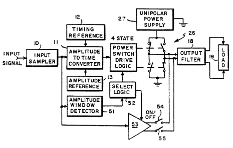
A quaternary switching amplifier in accordance
with the invention is shown in Fig. 7. As can be
seen therein, the complete circuitry of a ternary
amplifier is retained and the signal is processed
thereby in the same manner. An amplitude window
detector 51, decision making select logic 52, and a
separate linear amplifier 53 and switches 54 and 55
WO 92/12572
PCT/l'S91 /08377
- 22 -
associated therewith for turning the output thereof
on and off, are also used. Further, the output
switch device drive logic circuit is modified to
provide a capability of turning,all the switches to
their off state so as to implement the fourth state.
The output switch states are shown in Fig. 8. In
many cases it is possible to implement the two
switches 54 and 55, shown at the output of the linear
amplifier 53, without the need to use active switch
elements as shown. For example, the linear amplifier
can be modified to include suitably connected diodes
in its output circuit, as would be well known to the
art, the amplifier output being turned on and off by
low level internal switches that back-bias the output
diodes when the linear amplifier is not being used.
Tt should be noted that in, the switching circuit
shown in Fig. 7, other types of amplifiers could be
substituted for linear amplifier 53, although the
specific implementation shown in the figure
effectively addresses an important application
wherein relatively small signals are present, as
found in audio systems and in null servo systems, for
example.
The output of the switch circuitry in Fig. 7 is
applied to an output filter 18 and then to a load
19. The requirements for the output.filter are
further simplified from that used in a ternary
switching system. Since the low level signals from
the amplifier no longer have any switching transients
to produce a ripple, the errors produced by the
WO 92/1257?
PC'f/ l'S91 /083~ 7
- 23 -
filter operation do not appear when using the fourth
state. Moreover, when the output is switching, as
for large input signals, the ripple that is present
for large signals appears as a much smaller error
relative to the outputs being generated.
FIGS. 9, 9A, 9B and 9C show a simplified
presentation of the signals at various stages in the
quaternary switching amplifier. For the example
depicted, the use of a sampling circuit is shown in
the amplifier as a comparison to the ternary case.'
In many cases, as discussed above, such a sampling
circuit may not be needed.
As in the ternary case, the input signal 60 can,
be sampled and the sampled signal 61 held for the
conversion process which follows. The sample signal
61 is then compared to an internal reference
triangular waveform 62 just as in the ternary case.
This process and its resulting switch command output
63 (FIG. 9B) is shown in the first sample frame in
the figures. At the end of the first frame, in the
example shown, the input signal is less than the
window amplitude level limits 64 (FIG. 9A) being used
by the amplitude window detector 51 and remains
within the window limits during the next three frames
(frames 2, 3 and 4). As a result the select logic 52
now commands the switches to be in the fourth state
mode so as select the output of the linear amplifier
during the next three frames. Thus, the outputs 65;
65A, and 65B during such frames are the outputs from
the linear amplifier 53. In the frame (frame 5)
following such three frames, however, the detector
WO 92/12573
PCT/ l.'S91 /083 ; 7
- 24 -
detects a sampled signal that is again bigger than,
i.e., outside, the window limits. The select logic
52 then arranges the output to return to the ternary
mode so that the output again becomes the pulse width
modulated signal 66 (FIG. 9B) from the ternary
switching portion of the amplifier system.
The composite output is applied to the output
filter and the load, as in the ternary case. The
resulting output signal 67 (FIG. 9C) is then a
substantial replica of the input signal with a
superimposed ripple component.
When operating in the ternary mode for large
signals (greater then the "window" at the detector
51) the quaternary amplifier has all the properties
of a ternary amplifier including its high efficiency
and damping operation, as discussed above. When in
the fourth state, for small input signals (within the
window'), the quaternary amplifier has all the
properties of the linear amplifier (or whatever type
of amplifier is used), including low distortion and
error and further including the desired damping since
the linear amplifier also presents a low impedance to
the input of filter 18 as required for such damping.
Any inefficiency penalty imposed by the addition
of the linear amplifier can be made relatively
small. If the switch over to the fourth state is
done for signal amplitudes that are a selected
fraction of the total amplitude signal range, for
example 1/4, the amplifier used in the fourth state
need only handle 1/l6th of the total power at the
'CVO 92/ i 25''_ ~~ ~ ~ ~ PCT/ l.'S91 /083 ~ 7
- 25 -
maximum amplitude. The power inefficiencies in the
fourth state are thus related to a level that is 1/16
of the maximum power, rather than to the full power
amount which would be involved when using only a pure
linear amplifier over the entire range. The total
power penalty imposed is therefore relatively small
and allows the use of a relatively small and
inexpensive linear amplifier.
Another advantage of the quaternary switching
amplifier involves the use of the sampling circuit at
the input thereto. One of the reasons a sampling
circuit is used is to prevent false analog to digital
conversions near zero inputs that could result if the
signal were stewing or had significant noise. Since
conversion is no longer being performed near zero
input signal levels (i.e., in the fourth state), it
is possible to eliminate the sampling circuit in many
cases. Such elimination results in significant
performance benefits since it not only removes
another source of error in the signal path but it
also allows an increase in the bandwidth of the
overall amplifier, thereby permitting the use of a
wider feedback bandwidth for reducing any
non-linearities in the conversion process.
In order to provide the most effective operation
of such a quaternary switching-amplifier, it is
desirable that certain characteristics of the ternary
switching-amplifier and of the linear amplifier be
matched. Thus, the designs thereof should be such
that the transient responses, the frequency
responses, the gains, the D.C. biases, and the source
WO 92/12573 ? ~ ~ ~ ~ ~ ~ PCT/L~S91/08377
- 26 -
impedances of such amplifiers are matched as
effectively as possible. Design of the circuitries
thereof so as to provide the required characteristics
for each in order to produce,,such effective matching
would be well within the skill of those in the art
and need not be described in further detail here.
It is understood that the specific embodiments
described above represent exemplary embodiments of
the invention and that modifications thereto may
occur to those in~the art without departing from the
spirit and scope of the invention. Hence, the
invention is not to be construed as limited to the
particular embodiments disclosed herein except as
defined by the appended claims.