Note: Descriptions are shown in the official language in which they were submitted.
WO 92/12536 PCT/LrS91/04512
_i-
~.l.c~aAs Native Oxide
This invention was made, in part, with Government
support under contract DAAL 03 89-K-0008 awarded by the
United States Army and Grants NSF ECD 89-43166 and NSF DMR
89-20538 awarded by the National Science Foundation. The
Government has certain rights in the invention. This appli-
cation is a continuation-in-part of U.S. patent application
Serial No. 636,313 filed December 31, 1990.
BACKGROUND OF THE INVENTION
1. Field of the Invention
The present invention relates to a method of form-
ing a high quality, stable and compact :native oxide layer
from an aluminum-bearing Group III-V semiconductor material.
T~lore specifically, the present invention forms the native
oxide layer by a method involving wet thermal oxidation.
Importantly, the thickness of the native oxide layer produced
by the method is substantially the same as or less than the
thickness of the aluminum-bearing Group III-V material layer
that converts to the oxide. Further, the present invention
forms the native oxide under conditions that discourage the
formation of various other oxygen-rich compounds, such as
aluminum oxide hydrates and aluminum suboxides, the presence
~f which compounds cause an expansion oi: the resultant native
oxide layer thickness and are generally deleterious to the
electrical and physical properties of the semiconductors.
The present invention is also directed to devices
utilizing the native oxide'layer thus grown, including elec-
trical and optoelectrical devices such as transistors, ca-
pacitors, waveguides and, more especial7.y, lasers.
WO 92/ 12536 '' - PCT/ L.TS91 /04512
~~~~,~~ J
Finally, the present invention relates to the mash-
ing and passivation of semiconductors utilizing the native
oxide that forms from the practice of the present invention.
2. Description of the Prior Art
An important trend in semiconductor technology is
the use of Group III-V materials for the fabrication of semi-
conductor devices. While the utilization of silicon (Si) is
still prevalent in this area, Group III-V compounds --such as
GaAs-- have been the subject of much research due to the
significant advantages these compounds offer. For example,
Group III-V compounds generally exhibit larger band gaps,
larger electron mobilities and have the ability to produce
light, which properties result in unique electrical and opti-
cal characteristics.
Notwithstanding these qualities, Group III-V semi-
conductor technology has failed to develop at the rate and to
the level of silicon-based technology. The primary causative
factor to this end has been the inability to produce, on the
Group III-V semiconductor, an oxide layer of desired thick-
ness that exhibits the necessary surface state and electrical
properties required for practical application. In this re-
gard, the oxide must be able to fulfill, without the disrup-
tion and strain caused by over-expansion of the oxide thick-
ness, a variety of functions in a practical and consistent
manner. Examples of these functions include: serving as a
mask during device fabrication, providing surface passiva-
tion, isolating one device from another (dielectric isola-
tion, as opposed to junction isolation), acting as a compon-
ent in the anatomy of various device structures and providing
electrical isolation of multilevel metallization systems.
Accordingly, the presence of a high-quality, stable oxide
WO 92/12536 -3 PCT/US91/04512
layer having adequate physical properties and proper thick-
ness is essential to the successful development of Group
III-V semiconductor technology.
Silicon-based materials, unlike Group III-V semi-
conductors, readily form a high quality oxide (Si02) by such
methods as reacting the silicon crystal with water vapor,
.
e.g., in the form of steam. Indeed, the very existence of
silicon-based integrated circuit technology is largely due
and owing to this ability of silicon to form a high quality
silicon oxide. Moreover, this oxide is a native (or natural)
oxide, as opposed to a deposited oxide layer. Native oxides
are more desirable than deposited oxides in that they are
monolithic with the crystal and thus avoid potential mis-
matching of dielectric characteristics and problems asso-
ciated with oxide-substrate interface bonding, such as lift-
ing and cracking. Further, deposition processes are on the
whole more complicated and costly than are methods of growing
a native oxide thus making the latter more attractive for
commercial use.
Attempts at producing a ,qualit-y native o::id~ layer
on Group III-V semiconductors by adapting methods that have
been successful for silicon have had disappointing results.
These results are usually ascribed to the fact that the be-
havior of Group III-V materials depends, in large part, on
the behavior of the individual Group I:II-V constituents,
which behavior, under given circumstances, may not be compat-
ible with the desired end result. For example, thermal oxi-
dation techniques, which are regarded to be among the sim-
plest of the techniques and which have had tremendous success
for silicon, have not worked well for Group III-V materials
such as GaAs. This is because gallium (Ga) and arsenic (As)
have different oxidation rates, and because the AsZ03 and
4 As20~ that are produced in the normal course of events, are
~~~9~~~ _.
WO 92/12536 PCT/US9l/04512
v~iatile: once formed, they tend to boil off the substrate
rather than stabilize on it as part of an oxide layer.
Thus other approaches, which for the most part
occur at low temperatures, e.g., room temperature, to avoid
the formation of volatile components, to produce a native
oxide layer directly from a Group III-V semiconductor surface
have evolved. These techniques include the use of ozone,
simultaneous OZ and electron beam exposure, photo-excitation
of electron-hole pairs (in GaAs), use of more reactive oxi-
dizers (such as N?O), photochemical excitation of the gas-
phase molecular species, addition of water to the 02, excita-
tion of 02 with a hot filament or a Tesla discharge, plasma
excitation of the 02 a:.d exposure to a high kinetic beam of
atomic oxygen. The drawback of these techniques, aside from
their overall complexity, which makes them unrealistic for
large scale utility, is that although they can increase the
rate of formation of the first few monolayers of oxide they
are (with the possible exception of plasma oxidation and
exposure to a high kinetic beam of atomic oxygen) generally
ineffective for rapidly growing layers having a thicknesj ir.
the range of hundreds to thousands of angstroms, A (10,000 A
- 1 micron, urn). Moreover, these oxidation reactions are
often incomplete, the Ga and As not being in their highest
formal oxidation state. The resulting oxide is thus usually
deficient in Ga or As, which deficiencies have adverse ef-
fects on oxide quality.
Particular examples of these methods include: U.S.
Patent No. 3,859,178 wherein an oxide is grown on the surface
of a GaAs layer by submersing the GaAs layer into an anodiza-
tion bath of.concentrated hydrogen peroxide (H202) having a
pH of less than 6.
W092/12536 ~5 . PCT/US91/04512
'J.S. Patent No. 4;374,867 describes a method of
growing an oxide layer on InGaAs by using a growth chamber
that has been evacuated and in which an oxygen plasma has
been established. Water vapor is introduced into the chamber
to facilitate the growth process.
U.S. Patent No. 3;890,169 relates a method of form-
ing an oxide on GaAs in an electrolytic fashion using H202 as
an electrolyte. The oxide thus formed is rendered more sta-
ble and more impervious to impurities and dopants normally
employed in diffusion processes by being dried in oxygen at
250°C for 2 hours followed by annealing at 600°C for 30 min-
utes.
U.S. Patent No. 3,914,465 describes a double oxida-
tion technique whereby a native oxide is grown on GaAs by
immersion in an aqueous H202 solution with a pH of 1.5-3.5,
followed by a second oxidation in aqueous H2o2 at a pH of
6-8.
H. Barbe, et al. in Semiconductor Science and Tech-
nol.ocrv, 3, pp. 853-858 (1988) describe the growth of a thin
oxide layer on GaAs in methancl having a varying wate,_- con_
tent, without the application of external voltage. J. P.
Contour, et al. in the Japanese Journal of Applied Physics,
Vol. 27, No. 2, pp. L167-L169 (Feb: 1988) report on the prep-
aration of a surface oxide on a GaAs substrate by heating the
substrate to 250° - 350°C in air. Similarly, in Applied
P~sics Letters, Vol 26, No. 4, pp. 180-181 (Feb. 15, 1975),
the growth of an oxide film on GaAs by thermal oxidation at
350°, 450° and 500°C is described. Applied Physics
Letters,
Vol. 29, No. 1, pp. 56-58 (July 1, 1976) reports on a one
step dry process to form an oxide film on GaAs by plasma
oxidation using an oxygen plasma.
Because of the complexity of these techniques and
a the less-than-desirable results in terms of physicality and
WO 92/12536 ~ ~'J ~ c~ 6 PCT/US91/04512
ch.ickness obtained, all of which can be related to the diffi-
culties in worl~:ing with Ga and As, methods of oxide formation
have been developed which involve overlaying or implanting on
a Group III-V surface a material that can oxidize more read-
ily. Aluminum (Al) and aluminum-bearing compounds are ex-
amples of such materials. These particular materials are
particularly adaptable in that aluminum is a Group III ele-
ment and is known to oxidize more easily than the other ele-
ments normally found in Group III-V semiconductors.
Examples of oxidation methods which exploit the
presence of aluminum or aluminum-bearing compounds include
U.S. Patent No. 4,144,634 which first deposits a thin layer
of Al by, e.g., evaporation, over a GaAs substrate. The A1
overlay is then oxidized by plasma oxidation. Y. Gao, et al.
report in the Journal of Applied Physics, 87, (11), pp. 7148-
7151 (June 1, 1990) a cryogenic technique whereby molecular
oxygen is first overlaid on a GaAs surface; deposition of A1
follows. The A1 reacts to form an oxide layer until the
oxygen is depleted.
C. W. Wilmsen, et al. in Thin Solid Fplms; ~1, gp.
93-98 (1978) report a method whereby a metal, such as Al, is
implanted into a Group III-V substrate; oxidation then occurs
by thermal or anodic means. M. Hirose, et al. relate in
Physica Status Solidi, (a) 45, pp. P,175-K177 (1978) an oxi-
dation process for GaAs in which oxygen gas, admitted close
to the substrate surface, is reacted with A1 molecular beams
to form A12o3. Finally, U.S. Patent Nos. 4,216,036 and
4,291,327, and European Patent Application 0 008 898 describe
the fabrication of oxides by the thermal oxidation of an AlAs
or AIGaAs layer which has been epitaxially grown on GaAs.
The oxidation occurs in a flowing gas mixture of 800 02 and
20o N2, and can occur in the presence of water vapor in order
to permit the use of lower temperatures, e.g., 70°-130°C; the
WO 92/12536 -~- PCT/US91/04512
~~9~~~
oxides produced by this method ar~~, however, believed to be
aluminum arsenic oxide and/or hydrated aluminum oxides.
These types of oxygen-rich 'aluminum compounds do not have the
o requisite physical characteristics tlhat are necessary for
semiconductor application; moreover, their presence in any
modest amounts is deleterious to semiconductor structure. In
addition to this, and integrally related to the presence of
hydrator, is the expansion of thickness in the final oxide
layer, which is consistently 80o thicker than the thickness
of the original AlAs epilayer. In terms of real application
and device construction, this magnitude of layer expansion is
wholly impractical in that it distorts and strains the device
architecture to unacceptable levels acrd puts inter-dependent
dimensions and geometry out of kilter. These shortfalls are
especially harmful when the semiconductor device is an opto-
electrical device such as a laser, th.e optical output effici-
ency and lifespan of which is highly dependent on proper
crystal dimensioning and geometry as the various layers are
developed over the course of device fabrication.
In brief , prior art i"et hods which rely on the pres-
ence of materials such as aluminum, are either too complex
f or large scale use or result in oxides that contain signifi-
cant amounts of hydrates and/or have thicknesses which are
over-expanded. The oxides produced by these methods also
have less-than-desirable physical and electrical character-
istics, in that they have poor electrical properties, e.g.,
significant leakage, and the overall quality of their physi-
cal state is not good. As to the latt=er, oxides formed by
these known methods exhibit non-uniformities in density and
continuity, and also lack suitable stability, which results
in lifting, cracking and out-diffusion; devices fabricated
with oxides grown by these methods show a strong tendency to
degrade in unacceptably short periods of time under normal
WO 92/12536 R PCT/US91/04512
conditions of use and atmospheric exposure. These undesir-
able end results and deleterious effects thus preclude t:~e
use.> of these methods in large scale practical application as
required for commercial devices.
Thus the semiconductor art, although producing a
variety of methods to form oxides on Group III-V semiconduc-
tor materials, recognizes a continuing need for a method of
growing an improved, high-quality native oxide on aluminum-
bearing Group III-V semiconductor materials, particularly a
native oxide whose thickness is substantially the same as or
less than the thickness of the semiconductor material from
which it forms. Moreover, it is desirable that the method be
simple, cost effective and produce the native o::ide consis-
tently in a controlled and repeatable manner.
SUMMARY OF THE INVENTION
A new method of growing a high-quality native oxide
on an aluminum-bearing Group III-V semiconductor has now been
developed. The native oxide thus grown exhi~its a proper
range of conversion thickness and has superior physical and
electrical characteristics as compared to oxides grown by
methods known heretofore. Specifically, the native oxide
layer grown by the method of the present invention has a
thickness which is substantially the same as or less than the
thickness of that portion of aluminum-bearing Group III-V
material from which it forms. The native oxide layer thus
grown is denser and more stable than oxide layers formed from
prior art methods, meaning, for example, that they do not
degrade under conditions of normal use and atmospheric expo-
sure. Further, the native oxide grown in accordance with the
present invention manifests operating and performance char-
acteristics that surpass those of any other currently used
WO 92/12536 -9- PCT/US91/04512
~~r:ide film. For example, the native oxides formed from the
present invention exhibit excellent metallizztion adherence
and dielectric properties. The native oxides formed by the
method of the invention are particularly useful in optoelec-
trical devices, such as lasers, which can tolerate oxide
a layer contraction but are acutely affected by over-expansion
in oxide layer thickness. Lasers thus fabricated are capable
of long-term, high power output before burn-out occurs.
In accordance with the present invention, a method
of growing a native oxide on the surface of an aluminum-
bearing Group III-V semiconductor material is provided. The
method comprises exposing an aluminum-bearing Group III-V
semiconductor material to a water-containing environment and
a temperature of at least about 375°C to convert at least a
portion of the aluminum-bearing Group III-V semiconductor
material to a native oxide. The native oxide is character-
ized in that the thickness of said native oxide is substan-
tially the same as or less than the thickness of that portion
of said aluminum-bearing Group III-V :semiconductor material
thus converted.
In further accordance with i:he subject invention
semiconductor devices utilizing the native oxide thus grown
are provided. Devices of particular applicability in this
regard include electrical and optoelec:trical devices such as
transistors, capacitors, waveguides and, more especially,
lasers.
In still further accordance with the instant inven-
tion the masking and passivation of se:miconductor5 utilizing
the native oxide that forms from the present method is also
described.
-10-
WO 92/12536 PCT/US91/04512
EFF:iRh DE~CRIF'TI023 OI' TF-;E DRAWINGS
Fig. l shows a thin platelet of disorder-defined
red-gap AlAs-GaAs superlattice (SL1) discs surrounded by
yellow-gap AlxGal-xAs (where x is about 0.8) after oxidation
by the present invention at 400°C and 3 hours in are atmos-
phere of nitrogen and water vapor. The top row of SL discs
(representing a coarse-scale alloy) had e~:posed cleaved edges
which were converted by the present invention to native oxide
to a depth of 24 ~.un beyond the crystal edge (indicated by the
small horizontal arrows). The oxide thickness of the 24~un
region was substantially the same as the thickness of that
portion of the original SL1 material that was converted. The
oxide was transparent in appearance.
Fig. 2 shows an AlAs-GaAs superlattice (SL1) after
oxidation by the present invention at 400°C and one hour in
an atmosphere of nitrogen and water vapor. Oxide conversion
into the edge region of the SL disc was 3 um (as indicated by
small horizontal arrows). The oxide thickness of the Sum
region was substantially the same as the thickness of that
portion of the SL that was converted.
Fig. 3 shows an AlAs-GaAs superlattice (SL2) after
oxidation by the present invention at 400°C and 4 hours in an
atmosphere of nitrogen and water vapor. SL2 was a finer
scale alloy than was SL1 and the oxide formation was 2-3 dun
into the edge of the SL disc. The oxide thickness of the 2-3
Wn region was substantially the same as the thickness of that
portion of SL2 that was converted. The slower conversion
rate even at a longer time period relative to SL1 in Figs. 1
and 2 was due to the finer alloy scale of SL2.
Fig. 4 shows the photopumped room temperature (300°
f;elvin, K) laser operation of the red-gap SL1 discs of Fig. 2
which were oxidized by the present invention. The sample was
WO 92/12536 PCT/US91/04512
,~,
compressed in an annealed copper heat sin) under a diamond
window.
Fig. 5(a) is a scanning e:Lectron microscope photo-
mic:rograph showing quantum well heterostructu.re (QWH); the
lef t side of Fig . 5 ( a ) shows the QWF~ with an Si02 mash: ; the
right shows the QWH with the GaAs cap removed. The exposed
crystal where the GaAs cap was remo~~ed was oxidized according
to the present invention at 400°C for 3 hours in an atmos-
phere of nitrogen and water vapor. Fig. 5(b) shows the QWH
after the oxide on the right side wa.s selectively removed.
The slanted arrow in rig. 5(b) shows the crystallographic
facet defined by the natural oxide on the AlvGal-BAs (x or
abo'st 0 ~ 8 ) conf fining layer .
Fig. 6(a) shows the current versus voltage (I-V)
characteristics for the contact on the GaAs cap layer of the
left-side masked region (Si02 removed) of the QWH of Fig. 5;
Fig. 6(b) shows the I-V characteristic for the contact of the
right-side, region having the native oxide as formed accord-
ing to the present invention. Fig. ~(a) exhibits p-n conduc-
tion and Fig. 6(b) an open circuit (I ~ Ol.
Fig. 7 shows the spectral behavior and the power
versus current (L-I) characteristics of the QWH laser of Fig.
having the native oxide as grown according to the present
invention at 20 milliamps, mA, 30 mA and 40 mA.
Fig. 8 shows the high power laser operation of the
QWH laser of Fig. 5 which incorporates the native oxide as
formed according to the present invention. Burn-out did not
occur until over 100 milliwatts, mW/facet.
Fig. 9 is a photomicrograph showing the surface of
a multiple-stripe contact region, as prepared using a native
oxide that was f or;ned in accordance with the present inven-
tion, on a AlxGa1-xAs-GaAs (x of about 0.8) QWH crystal.
Fig. 9(a) shows the native oxide as formed at 400°C for 3
WO 92/12536 -1 ~' PCT/US91/0451Z
h~~urs i_n an atmo.spheze'ol'nitrogen and. water vapor, on the
upper AlYGa~ -3,As ( x, of about () . 8 ) conf fining layer ~,a;~ez a the
QWFI was not: ma~l:ed by a GaAs contac t layer . Fi.g. 9 ( b ) shows
the entire surface following m~tallization 4:ith titanium-
plati.num-gold (Ti-Ft-Au).
Fig. 10(a) shows the neap:-ffield (tdF), and Fig.
7.0(b) thc~ far-fie7_d (F'F) emission patterns of the ten element
Jrtl11t1p1E'-stripe ~WH laser array ShU47n 1:1 Fig. 9 which had 5
micron (um) wide emitters on 7 llm center-to-center spacings.
The narrow pea): with full angle at half power at 100 mA of
0.6° (Fig. 10(b)) indicated that the strips were coupled.
Fig. 11 shows the continuous-wave (cw) room-temper-
ature (3U0° K) laser operation of the ten emitter QWH coupled
array ~f Figs. 9 and J..O which had 5 um wide stripes on 7 um
centers. The output power per facet approached 300 mW. In
the inset, the spectral behavior tat 8457 ~ and 1.466 eV) of
the diode is shown at an output power. of lO mW (115 mA).
Fig. 12 shows the high power operation of a ten
emitter native-oxide coupled-stripe Al.l,Ga1-kGaAs QWH laser
array. The stripe width was the sa:~e as t hat of t~iie array of
Fig. 11 ( 5 dun) , but the stripes were located on 10 j.un cen-
ters, as shown in the inset. Output powers exceeding 400 mW
per facet were obtained.
Fig. 13 shows a shallow-angle beveled cross sec-
tion, after zinc (Zn) diffusion, of a 1.05 wn AlxGal-xAs-GaAs
superlattice with 20 um masking stripes, (top) on the crystal
surface. The masking stripes were comprised of a native ox-
ide as formed in accordance with the present invention. The
lower part of the slant cross section shows regions, not
masked by the oxide, where the superlattice was disordered;
the disordered regions are shown as alternating with regions
that were masked by the native oxide and where the super-
lattice was intact.
WO 92/12536 1 3 PCT/US91/04512
F'i g . 1 ~~ shows tl~e cleaved section of a ( i00 )
AlxGa1-hAs-F.lyGal-yAs-AlZGa1-BAs QWH (x of a3~out O.F, y o
about 0 . ?.5, z of about 0 . 06 ) ~>latelet sample. Native o::ide
formed according to the process of the present invention, was
revealed by removing the substrate and etching a tapered hole
through all the layers (stopping at the oxide). The native
~t:.ide layer, indicated as Region A, transmitted light an~? was
clear enough to show spocks of dirt 'that were on it. The
upper confining layer is indicated as Region B; the QWH wave-
guide and upper and lower confining :layers are indicated as
Region C. The,entire QWH is indicated as Region D.
Fig. 15 shows the photopumped continuous wave (cw)
room-temperature (300~ K) laser operation of the annealed QWH
of Fig. 14 which incorporated a native oxide as formed by the
method of the present invention: Fig. 15(b) shows, in com-
parison, the pulsed-excited laser operation of a non-masked
bare sample as modified by impurity-induced layer disordering
(IILD). Both samples had been simultaneously annealed at
575°C for 1 hour in a Zn diffusion ampoule.
Fig. 16 shows a scanning electron microscop' (;g~.~,)
Image (using a stain) of a buried-heterostructure (BH)
AlyC,a~-yAs-GaAs QWH laser of er Si di:~fusion at 850°C for o.5
hours and impurity-induced layer disordering on the left and
right sides (indicated by the letter "n"). Oxidation accord-
incT to the present invention, at 400°C~ and 3 hours in an
atmosphere of nitrogen and water vapor, of the top confining
layer was then performed. The Si diff:usion undercut the edge
of the GaAs cap, which resulted in a contact region of about
. 5 um and an active region of about 7 ~m ( f or a 6 lun masking
stripe). The formation of a native oxide by the method of
the invention was at. the surface of the exposed high-gap
Al~_Gal-xAs confining layer, and extended completely to the
w 14 - pCT/US91 /04512
WO 92/12536
edge of the Gams cap ( as indicated by the two unmar)~ed down-
ward arrows).
F'icr. 17 shows the continuous wave (cwl room-temner-
ature, (30f~° K) output (single facet) power versus current
(L-I) curve and spectra for a:~ IILD QW~i laser diode, having a
native oxide layer as formed by the method of the present
invention. '.Che laser diode had a 3 ~m-wide active region (as
compared to the 7 um wide active region of the laser of Fi.g.
16). The laser threshold (250 um long diode) was 5 mA, with
single mode behavior well developed at 7 mA (~;avelength of
about 8198 A). Spectral narrowing and "ringing" began at
about 2 mA and caused the fuzzy appearance at the top ef
curve (a) of the inset (3 mA).
Fig. 18 shows the near field (NF) and far-field
(FF) emission patterns of a 3-arm-wide active region IILD QWH
laser, that was delineated by native oxides as formed by the
present invention, under continuous wave (cw) excitation of
12 mA. The near-field (tZF) pattern indicated as (a), had a
full width at half maximum power of about 3.4 ~.~.m. The far
fif~ld ( FF ) pattern, i.,~ii~3ted as (b) , hau a iuii angle at
half power of 20.9°, and was diffraction limited.
F.ig. 19 shows a Nomarslsi image photograph taken
after 100 days of an AlAs-GaAs heterostructure which had
undergone oxidation at atmospheric conditions, Fig. 19(a),
and which had a native oxide layer as formed by the present
invention, Fig. 19(b). The atmospherically oxidized Sample
(a) shows the characteristic roughening of atmospheric hydro-
lysis, while Sample: (b) oxidized by the method of the inven-
tion was covered with a smooth "blue" oxide and was unaf-
fected by the aging process.
Fig. 20(a) is a scanning electron microscope (SEM)
image (unstained cross section) of Sample (a) of Fig. 19
W0 92/12536 ~ i S'~ PCT/US91/04512
,a° ~~~~i~~~
att~:t being cleaved and aged ('for,it)U days). Fig. 2U(b) is a
SEM image of Sample (b) of. Fig. 19 after being cleaved and
aged (for 100 days}. Sample (a) had been chemically attacked
tc~ a depth of 1 u.m ( indicated by vertical arrows } and was
striated in appearance. In contrast:, Sample (b) remained
smooth under the native o~.ide layer which was less than 0.1
urn thick. This thickness was less than the thickness of that
f>ortion of heterostructure which had. converted to the oxide.
Fig. 21 shows secondary ion mass spectrometer
(SIMS) profiles after Sample (a) and (b) of Fig. 19 were aged
for 80 days. In accord with the SEM images of Fig. 20, a Ga
depletion approximately 1 ~ deep in Sample (a) was not evi-
dent in Sample (b). Also in accord 'with Fig. 20, Fig. 21
shows that chemical attack was about 1 um deep for Sample
(a}; no chemical attack at this depth was evidenced in Sample
(b).
DETAILED DESCRIPTION OF THE INVENTION
The present i n«entl0n pr~~,~.d~g a mCth Od of forming
a high-quality native oxide from a Group III-V semiconductor
material where the thickness of the native oxide i.s substan-
tially the same as or less than the thickness of that portion
of said Group III-V semiconductor material which is converted
to the native oxide. The native oxide formed by the present
invention is especially utile in the fabrication of electri-
cal and optoelectrical active devices, including capacitors,
transistors, waveguides and lasers, such as stripe-guided
lasers, surface emitters and lasers whose active regions, as
normally defined by their quantum well structures, are
slightly mismatched in order to lengthen the wavelength of
the energy emitted. An example of su~~h a device is one hav-
WO 92/12536 1 s PCT/US91/04512
lng a f lrst quantum wc_ll 'i c>rmcd of , a . g. , InGaAs inside of a
second quantum well formed of, e.g., GaAs. The native oxide
formed by the method of the present invention can also be
used to define various geometries and patterns on the sur-
Faces of Group III-V semiconductor materials in order to
create any number of different configurations and topologies.
The method of the present invention finds
particular utility in forming a native oxide from an
aluminum-bearing Group III-V semiconductor material.
Although the scope of the present invention is independent of
any theory explaining its superior results, it is theorized
that the present invention forms the native o:,ide in a manner
that discourages the formation of debilitating amounts of
hydrated and/or oxygen-rich aluminum compounds that are
believed primarily responsible for the increase in thickness
of native oxide layers grown in accordance with wet thermal
oxidation techniques known heretofore, relative to the
thickness of that portion of aluminum-bearing material so
converted. In another aspect, it is believed that the
present inventio_n_ forms the native vxiue izi a manner that
favors the formation of sufficient amounts of anhydrous forms
of aluminum oxide and/or aluminum oxide hydroxides (referred
to herein as dehydrated aluminum compounds) such that the
thickness of the native oxide layer thus formed is
substantially the same as or less than the original thickness
of that portion of the aluminum-bearing Group III-V material
converted to the native oxide.
As to the aforementioned oxygen-rich aluminum
compounds, these include, e.g., compounds having the formula
A10, A120 and A12o2. These compounds, which are deleterious
t.o semiconductor performance and stability, are referred to
herein as aluminum suboxides.
WO 92/12536 ~ I ~ - PCT/US91 /04512
h~' ~f~?T-~'ment.~or~~d hvdrat:.ed compounds that-. arc
r>el.ieved to form in undesirable amounts when employing wet
t~»rmal o::idation methods known heretofore, and are
accordingl~~ believed to contribute to the poor quality and
increased thickness of native oxides thus formed, include
aluminum hydroxides and aluminum oxide hydrates as
hereinbelow defined.
As t0 alumiIlum hydroxides, the most well-defined
crystalline forms include the three trihydroxides having the
general formula A1(OH)3, which are conventionally denominated
as gibbsite (also known as hydragillite in European
literature), bayerite and norstranditn. The deleterious
effects of these aluminum hydroxides relative to
semiconductor application are believed related ~to the triply
hydroxylated status of the aluminum.
As to the aluminum oxide hydrates, these are formed
from the intermediate or transitional forms of aluminum
oxide; A1203. These intermediate forms, individually
unsuited for practical semiconductor purposes, are generally
i.den rifled as : '~ -A1_ p ~y _Al n ~ T ~ ~~ , ~-A i2'v3 , k-A12o3
j , ,.
and L,-A120.~. These intermediate species of aluminum oxide
normally exist between the compositional range of true
anhydrous aluminum oxide and the hydroxide forms of aluminum.
Accordingly, some of these intermediate species can form
hydrates of the formula A1203. nH20 (O<n<0.6). It is the
hydrates which form from these intermediate aluminum oxides
that are referred to herein as aluminum oxide hydrates. It
is further believed that the greater the degree of hydration,
e~g., trihydrate versus monohydrate, the greater the degree
of. expansion in native oxide layer thickness.
One technique of determining the extent of
hydration in an oxide layer is by meas~r,ring the index of
refraction (denoted as "n"), which those of skill in the art
WO 92/12536 18 PCT/US91/04512
tail? appreciate as c:orrelatab~.e to dielectric constant. As a
rule, the larger the index of refraction, the greater the
dogree of hydration of the oxide layer and the more
unsuitable that oxide is f.or practical semiconductor
application. Thus the index of refraction for hydrated
aluminum compounds such as, e.g., aluminum o3:ide hydrates, is
generally in the range of about 2.0 to about 11Ø In
comparison, the index ~f refraction for anhydrous oxides is
generally in the range of less than about 2.U. For example,
a dehydrated film of GaAs-oxide formed by gas plasma
c~xid.atioc~ has m index of refraction, as measured by
conventional ellipsometer techniques, of about 1.78 to about
1.87; dehydrated arsenic oxide (AsG03) has an index of
refraction of_ about 1.93. Generally, anhydrous aluminum
oxides and aluminum oxide hydroxides have an index of
refraction of less than about 2Ø
In addition to forming the native oxide in a manner
that discourages the formation of debilitating amounts of
hydrated ~~nd/or oxygen-rich aluminum compounds as
hPreinabeve described, it is beiiPVed teat the ~r~ser,t
invention forms the native oxide in a manner that favors the
formation of sufficient amounts of anhydrous forms of
aluminum oxide and/or aluminum oxide hydroxides to thus
obtain a native oxide having the requisite physical and
electrical properties required for practical semiconductor
application, as well as a thickness that is substantially the
same as or less than the thickness of the aluminum-bearing
material that is converted to native oxide by the practice of
the present invention.
In this regard, a native oxide thickness that is
substantially the same as or less than the thickness of the
aluminum-bearing material that is converted can be measured,
for purposes of the present invention, by the ratio of native
WO 92/ 12536 ' 1. 9 - PCT/US91 /04512
u~:ide tti.ic~:ness to the thic~:ness of t:he aluminum-bearing
material thus converted. As contemp3.ated by the present
invention, this ratio is within the range of between about
0.G to about 1.1 (representing a shrinkage of the native
oxide layer compared to the portion of aluminum-bearing
material so converted of about 400, t;o an expansion of the
seine of about 10 ~) without adversely affecting the physics of
the native oxide formed:
As to the anhydrous forms of aluminum oxide, these
. include a,-A1z03 and ~ -A1203. It is important to the
appreciation of the present invention, to understand that
stoichiometrically there is only one oxide of aluminum
--namely, A12O3-- and that this oxide is polymorphic: it
eyists in a variety of crystalline forms which have different
structures, most of which, such as e.g., the intermediate
aluminum oxides identified hereinabove, are substandard
insofar as useful semiconductor-related electrical and
physical properties are concerned. Generally, the forms of
aluminum oxide that manifest the highest degree of parameters
iWCcssary fvr practical sen~icvnC3iit:tor applicati~il ale ti'1~
anhydrous forms, including a-A1203 and. ~-A1203.
For- example, a-A1203 .has a well-defined, close
packed lattice arrangement, and exhibits extreme hardness,
stability, resistance to wear and abrasion, chemical
inertness (including insolubility in, and unreactivity
toward, water), outstanding electrical properties (such as
dielectric character), good thermal shock resistance,
dimensional stability and high mechanical strength.
As to aluminum oxide hydroxides, these include the
two well-defined crystalline phases having the general
formula A10(OH) which phases are convE:ntionally denoted as
diaspore and boehmite.
WO 92/ 12536 ~ ~ 2 ~ PCT/US91 /04512
I ~. i s t~el i eveci tluat the native oxide formed in the
gracticc: of the prosent, ~invc:ntion is formed in a manner
such t3~at suffic:LCnt amounts of the anhydrous forms of
aluminurc~ oxide and,~or aluminum oxide hydroxides result,
rather than debilitating amounts of the hydrated and/or
oxygen-rich aluminum compounds, and further believed that
this circumstance is manifested in the fact that the
thickness of the native o:,i.de formed in the practice of the
~~rosent invention ~.s substantially the same as or less than
tlne thickness of the aluminum-bearing material that is so
converted.
Molar volume serve~~ ;:. an indicator in this regard.
That is, the fact that the thickness of the native axide of
the present invention is substantially the same as or less
than the thickness of that portion of the aluminum-bearing
mater:i.al treat converts to the native oxide is believed to
indicate that the present invention farms a native oxide of
compounds that have a molar volume substantially the same as
ur less than that of the almnimun-bearing Group III-V
SCmICOnduCtOr materi 31 from lr7h.l.Ci: t he iiati'vC 'vYide forms.
Molar volume can be established from the following
formula:
Molar Volume = Molecular Weight - Density
The molar volumes for AlAs (an aluminum-bearing
Graup III-V material contemplated by the instant invention),
a-A1203 and ~-A1203 (anhydrous forms of aluminum oxide, as
defined by the present invention), diaspore (an aluminum
oxide hyd.ro::ide, as defined by the present invention) and
gi.bbsite (an aluminum hydroxide, as defined by the present
invention) and aluminum mono- and tri-hydrate (aluminum oxide
hydrates, as defined by the present invention) are listed in
Table 1; below:
WO 92/12536 21 - PCT/US911045t2
~~~ ~ig~
Ti:t3LE J:
Molar thvlecular
Substance Weiaht, a Density, yolume,
alca c/mol
c
n-A1203 101.96 3.5 - 3.9 29.1 - 26.1
~j-A1203 101.96 3.97 25.7
gibbsite, A1(OH) 78 2
3 52
_ . 32.2
diaspore, A10(OH) 60 :l
3 - 3'
5
. 18.2 - 17.1
.
aluminum trihydrate, 156 2
42
. 6s.5
A1203 3H20
aluminum monohydrate, 199.98 3 '
014 g
. 3
A1203. F120 ,8
AlAs 101.90
3.73 27.3
GaAs 144.64 5:316 27,2
As seen by reference to Tab_Le 1, the molar volumes
of the anhydrous forms of aluminum ox»de, a- and ~ -A1203,
and the aluminum oxide hydroxide, diaspore, are substantially
the same as or lE:SS than that shown for AlAs, thus indicating
that an oxide formed from AlAs in practicing the present
invention, wherein the native oxide ha.s a thickness
substantially the same as or less than that portion of AlAs
form which it forms, may be comprised primarily of dehydrated
aluminum compounds, i.e., the anhydrous forms of aluminum
oxide and/or aluminum oxide hydroxide. In contrast, when the
thickness of the native oxide formed from AlAs is greater
than that portion of AlAs thus oxidized --as in the case in
earlier attempts at producing a native oxide, such as by
methods embodied in U.S. Patent Nos. 4,,216,036 and
4,?_91,327-- this is believed to indicate that the native
PCT/US91 /04512
WO 92/12536
~xi~e thereof is comprised primarily of compounds whose molar
volt.une i.s greater than AlAs , such as , a . g . , aluminum
monohydrate, aluminum trihydrate, and gibbsite --an aluminum
hydroxide.
irr~ilar to aluminum, gallium also forms a.n oxide,
Ga20.~, that has a variety of crystalline forms; these cry-
stalline modifications are denoted a-Ga?,03, 8-Ga20.~,
-Ga2U3, d -Ga203, e-Ga203. Of these, B-Ga203 is the most
stable and best suited for semiconductor use. Further, under
proper circumstances, aluminum oxides, such as a-A120.~, and
gallium oxides, such as B-Ga?03, can form a solid solution
and can form compounds of the formula GaAlO.~.
In the practice of the present invention, a native
oxide is formed from a Group III-V semiconductor material;
preferably an aluminum-bearing Group III-V semiconductor
material such as, e.g., AlGaAs, AlInP, AlGaP, AlGaAsP,
AlGaAsSb, InAIGaP or InAlGaAs.
In a practical embodiment of the present invention,
the alumini:m-bearing Group III-V semiconductor material is
overlaid on the surface of an al~~min~,:,~"-free Group III-V semi-
conductor material such as, e.g., GaAs, GaP, GaAsSb, InGaP or
InGaAs. When the thicl>ness of the aluminum-bearing overlayer
iS IlOt :;o great so as to impede the diffusion of the neces-
s~~?-y oxidation reactants down through the entire aluminum-
bearing layer, the conversion of the aluminum-bearing layer
t_o the native oxide layer will essentially terminate at the
aluminum-free Group III-v interface, or when the aluminum
content of a given layer or interface 1_ayer is about 300 or
less, e.g., x is about 0.3 in material such as AlxGal-xAs.
Diffusion effects, which can eventually terminate the
oxidation reaction, normally become a factor when the
aluminum-bearing material has a thickness of about 10,000
or more.
WO 92/12536 ?' PCT/US91/04512
Tt~c method ~f the present invention entails expos-
:incr the aluminum-bearing Group ILI-V' semiconductor material
to an environment. that contains water, preferably in the form
of water vapor. In the preferred practice of this embodiment
of the invention, the water vapor is present with one or more
inert gases, such as nitrogen: The water vapor is also pre-
ferably present in an amount wherein the nitrogen or other
inert gas or gases is substantially saturated with water.
The water-containing inert gas environment is preferably, but
need not be, under a condition of flow. When under flow, the
rate should be at least about 0.5 standard cubic feet per
hour (scfh), preferably about l.0 - :3.0 scfh; most preferably
about 1.5 scfh.
In practicing the present :Lnvention, ~a temperature
of at least 375°C is employed. Although no specific time
period need elapse in order for the native oxide to form in
the first instance, certain practices in this regard are
preferred, especially in applications involving the more
typical aluminum-bearing Group III-V semiconductor materials,
such as A1~Gal-XAs where x is about i~.7 o_r greater-
Thus in a first embodiment of the present inven-
tion, wherein the temperature employed is in the range of
from about 375°C to about 600°C, preferably in the range of
about 390° C to about 500°C, more preferably in the range of
about 400°C to ai~out 450°C, it is preferred if the exposure
to the water-containing environment is for a time period of
about 0.1 hour to about 6.O hours. A more preferred time
period far this first embodiment is about 1.0 hour to about
5.0 hours; even more preferred is a time period of about 2.0
hours to about 4.0 hours. Most preferred for this first
embodiment is a time period of about :3.0 hours.
In a second embodiment of the present invention,
referred to herein as rapid thermal processing, a temperature
WO 92/12536 ~ z 4 ~ PCC/US91/04512
,~z
.i.n ~..lm 1 mr~c~c~ c~f ov:~r abc~m GOU°C t~~ about 22UU°C. is
emplolTed.
I n a yre,i_-err ed aspect of tlni.s second embodiment, the
tomnerature employed is in t.hc range of about 650°C to about
1000°C; more: preferably about 700°C to 900°C and most
preferably about X00°C.
In the practice of this second embodiment of the
~.>resent invention the exposure to the water-containing
environment will depend upon whether the material is
self-capping under the conditions employed. If not, exposure
is preferably for a time period of up to about 120 seconds.
A more preferred time period for this second embodiment is
about 5 seconds t.o about 90 seconds; even more preferred is a
ti~«e period of about 10 seconds to about 50 seconds with the
most preferred time period for this second embodiment being
about 15 to about 30 seconds.
The time periods preferred in the practice of this
second embodiment of the present invention are abbreviated to
account for the fact that certain Group III-V materials, such
as arsenic, have a tendency to evaporate at the higher tem-
peratures employed therein. Thos the short exposure tim2S
fc>r these materials that are not self-capping are preferred
in order to prevent or minimize any such losses.
In the practice of the present invention,
particularly in the practice of the second embodiment
described hereinabove, material to be oxidized in accordance
therewith may be exposed to the aforedescribed temperatures
in the first instance, or alternatively, may be heated to
these temperatures from a lower temperature, e.g., room
temperature (about 20° - 25°C) in heating apparatuses, such
as conventional annealing furnaces or ovens, that are capable
of reaching these temperature ranges in about 2 seconds or
less, preferably in about 1 second or less.
In any event, in practicing the present invention
the temperature need not be hci4 co:~stant. Thus for example,
2a~~a~~
WO 92/ 12536 ~ ' ' - PCT/US91 /04512
within the ranges elucidated above the temperature may be
ramped up or down. These t.ernperatune ranges axe believed to
discourage any appreciable formation of hydrated aluminum
compounds and/or aluminum subo:sides iri quantities that would
deleteriously affect the final oxide and its utility for
semiconductor purposes. At the same time, these temperature
ranges are believed to encourage the formation of the
desirable anhydrous forms aluminum o:y:ide, such as a-A1?03
and/or aluminum oxide hydroxides, such as diaspore.
Other processing may occur subsequent to exposure
of the aluminum-bearing Group III-V material to the water-
containing environment without detrirnentally affecting the
native oxide that has formed. Thus t=he native'oxide and the
structure or article on which it has formed may be dried by
removal from, or removal of , the water-containing environ-
ment, with heating being continued at: the same or different
temperatures than those used to form the oxide. Inert gas
may also be passed over the native oxide-containing structure
to facilitate drying. For example, in a flowing water vapor-
nitrogen (or other inert gas) system at a temperature of,
e.g., about 400° to 450°C, the flow of.water vapor into the
system may be stopped after, e.g., 0.25 hour; the flow of
nitrogen gas continuing however for a period of time there-
after, e.g., 2 hours. The temperature of the flowing nitro-
gen system may be the same temperature as used during oxide
formation, or the temperature can be :ramped up or down, e.g.,
from 450° to 500°C.
Other processing that can occur subsequent to oxide
formation and which has no ill-effect on the quality of the
native oxide includes annealing. As conventionally preformed
for_ Group ILI-V semiconductor materials, annealing takes
place under "dry" conditions; that is in the absence of
water. Dry conditions in this regard normally entail the use
WO 92/12536 ~ ? '~ PCT/US91/04512
o.f an )s? ~~ar environment. ~~nnealing can also take place
under an ovrr-~~re~ssure formed of materials having a tendency
to vaporize at the thermal conditions employed to anneal.
Thus the native oxide-containing structure may be sealed in
an ampoule having, optionally, an overpressure of arsenic or
phosphorous; the former being normally used for arsenic-
containing Group III-V semiconductor materials (such as
AlGaAs) the latter for phosphorous-containing Group III-V
semiconductor materials (such as InGaP). Annealing is in
either case generally performed at a temperature of about
600°C to about 850°C, preferably in the higher temperature
ranges, e.g., 850°C, for a time of about 0.25 hour to about 4
hears, normally.
The .fol7.owing Examples are given to illustrate the
scope of the present invention. Since the Examples are given
for illustrative purposes only the invention should not be
limited thereto.
2fl_9fl~8
WO 92/ 12536 2 ' - PCT/US91 /0451 Z
F~~AMPLF' 1.
OY>>IUA~~ION OF' A1',Ga As-AlAs-GaAs
1. - x
9UANTUM WELL ~IETEROSTRUCTURES ArdD SUPERLATTICES
AlAs-GaAs superlattices (S:Ls) were grown by metal--
organic chemical vapor deposition techniques, as described by
R. D. Dupuis, et al. in Proceedings c~f the International
Symposium on GaAs and Related Corwounds, edited by C. M.
Wolfe, (Institute of Physics, London,, 1979), pp, l-9 and by
I~1. ,7. Ludowise , J . Appl . Phys . , 58 ,W31 ( 1985 ) . Several SLs
were employed, each about i micron (Lun) thick. Superlattices
denoted as SL1 had AlAs barriers having an LB size of about
1 ~0 ~~, and Ga7ss wells of width LZ of about 45 A~. Superlat-
tices denoted as SL2 had an LB(AIAs) of about 70 A and an
Lz ( GaAs ) of about 30 ~,. Although sub>erlattices have a spe-
cial character, i.e., sine quantization, they are also re-
garded as being relatively "coarse", i.e., non-stochastic,
AlyGal-xAs alloys. In this Examp)_e, SL1 was roughly two
t vmes coar ser than SL2 . SL1 and cL~ ..,; ~-~. r , ",
~, "1~1. ~ l~u ~ surfaces,
were rendered into random, or fine scale alloys, in a pat-
terned form by impurity-induced layer disordering (IILD) by
zinc (Zn) diffusion from ZnAs2 at 575°C for 0.5 hour as
described by D. G. Deppe, et al. J. App).. Phys , _64, R93
11988) and W. D. Laidig, et al. Appl. phys. Lett., 38, 776
(1981).
The SLs were masked with Si02 discs having a dia-
meter of about 37 dun. The discs were deposited by chemical
vapor deposition and patterned (by standard photolithography)
i.n a rectangular array on centers of about 76 Wn. After the
Zn diffusion and the removal of the masking Si02, as well as
the removal of the crystal substrates (by standard methods of
WO 92/ 12536 ' '' PCT/US9t /045 t 2
mc.riuanical ldpping.and wet chemical etching), completely
smooth, yellow gars Al~,Gal-',As platelets (having a thickness
of about 1 'un) with red gap SL discs ( having diameters of
about 37 um) distributed in a uniform array were obtained, as
described by td. Holonyak, et al., Appl. Phys. Lett., _39, 102
(1981). The "fine" scale (yellow) and "coarse" scale (red)
alloy, were now all in one sample, which sample was oxidized
according to the method of the present invention: The sam-
ples were heated in a furnace at 400°C for 3 hours in an H20
vapor atmosphere obtained by passing N2 carrier gas (with a
flow rate of approximately 1.5 scfh) through an H.,O bubbler
i-
that was maintained at 95°C. The sample thus obtained by
th:Ls method formed a native oxide having smooth, shiny sur-
faces, which were much shinier than before oxidation. This
surface characteristic was indicative of a dense, compact
oxide that was substantially free of alumina oxide hydrates,
and that a major component of the native oxide thus formed
was likely an anhydrous aluminum oxide, such as a-A1?03.
A cleaved section of SL1, which was oxidized ac-
tor ding to the invent i on is sho;.;.~. ; ~ ~; -- , '~,_ -
~.. i .iy . t . lFle LOp edge o~
the 37 um diameter SL discs was cleaved and arranged so to
expose the edge of the SL samples (the discs) to the oxida-
tion process of the present invention. The bottom row of
discs was uncleaved and hence was exposed to the oxidation
process of the present invention only at the surface (front
and back). As Fig. 1 shows, the conversion of the cleaved SL
discs to the native oxide was to a depth of about 24 um as
measured from the edge of the SL (as indicated by the small
horizontal arrows). This oxide thickness was substantially
the same as the thickness of the cleaved, exposed SL that was
converted. No expansion of thickness for the native oxide
layer was seen. As to the bottom row of discs, only a slight
WO 92/12536 ? ~ PCT/US91 /04512
delineation of oxidation was evident on the periphery; some
surface oxide was also present. Thus after oxidation by the
method of the present invention, the upper row of discs ap-
peared solid and were nearly totally clear across each disc,
while the surrounding IILD Al~Ga1-xA.s (where x is about 0.8)
material remained yellow in appearance and the bottom row of
discs (SL1 with oxide surface) remained red.
By reducing the time of the oxidation process from
3 hours to 1 hour (all other parameters were the same), the
edge oxide conversion of an SL1 disc was to a depth of about
3 u.m as measured from the edge of the SL as shown in Fig. 2
(as indicated by the small horizonta:L arrows). This depth
(or thickness) was substantially the same as the depth (or
thickness) of that portion of the SL disc that~was converted
to the oxide. No expansion or increase in the oxide thick-
ness relative to the original SL thickness was seen. In Fig.
3, an SL2 (L~ + LZ being about 100 A) was oxidized for 4
hours, as opposed to the 3 hours in the case represented by
Fig. l.. Edge oxidation of an SL2 di~~c, which is a finer-scale
alloy than that represented by SL1, r~aS to ca dept h of ~-~ 4,U't1
as measured from the edge of the SL, even with the longer
oxidation time. Nevertheless, the 2-3 llm oxide depth was
substantially the same as the original SL thickness that was
converted to oxide. No increase or expansion of oxide depth
(thickness) was seen. The surrounding yellow gap AlxGal-xAs
material (where x was about 0.7) IILD alloy oxidized also,
but not nearly as extensively; oxidation here was hardly
noticeable at all except for the shiny surface. Thus a dif-
ference in the oxide conversion of (AlAs)x(GaAs)1-x alloy is
seen when progressing from a coarser scale to a finer scale
alloy, with random alloy and lower compositions converting
much "slower". In all cases, however, the thickness of the
WO 92/12536 ~.g .3~ PCT/US9t/045t2
~5:ide formed by r-he n~ct2uod of the invention was substantially
ty same as the thic~;ness of that por tion of the alloy tha t
converts to the o~:ide .
F'.ic~s. 1~-3 also show that there is major anisotrop;l
in h041 the o3:ide developed Un ( AlAs ) x ( GaAs ) 1-X SLs. O::i~da-
tion normal to the layers was much "slower" than along the
layers, and began to approach or become equal when the scale
of the SL was finer. This is seen by comparing Fig. 3 (SL2
with LB + LZ approximately 100 A) with Fig. 1 (SL1 wit.u LF +
L approximately X00 rg.) .
z.
Thc~ high duality of the oxide produced by the met-
hod of the present invention was demonstrated by way of a
photopumped laser. F'ig. 4 shows the photopumped laser opera-
tion of one of the inner (seal.ed edge) SL1 discs of Fig. 2;
the sample was heat sunk compressed in annealed copper under
a diamond window by conventional methods. The laser opera-
tion (at 300° k) of this SL sample was possible even with
the loss, by oxidation, of some of the layers on both sides
of the red gap SL disc, and even with some oxidation non-
uniformity at the disc peripr~ery because of the crystal a::d
doping difference (heavily p-type edge). It is believed that
these results are attributable, at least in part, to the fact
that the thickness of the native oxide produced was substan-
tially the same as the thickness of that portion of_ the cry-
stal that was converted to the oxide. That is, because the
thickness of the native o~>ide thus formed was substantially
the same as that portion of the SL layer that converted there
was no appreciable distortion of the laser structure, meaning
that high performance operation was possible.
WO 92/12536 " ~ n " PCT/LjS91 /04512
J'.;~:11t~9PT.F:. 2
NA'.L'IVE OXIDE-DEFINED SINGLE STRIPE GEOI'IETRY
tll .Ga. As-GaAs QUA2dTUIfi YELL HETEROSTRUCTURE LASERS
The use of native o ides f ormed in accordance with
tree present invention in the fabrication of gain-guided
oxide-stripe quantum well heterostructure (QWH) lasers was
investigated. These devices, formed by simplified process-
ing, were found to have outstanding performance character-
istics which were directly attributable to the quality of the
native oxide and the fact that the thickness of the oxide was
substantially the saime as that portion of the cr~Tstal that
was converted; thus the laser structure was not~distorted or
strained as would happen if the oxides thic?mess expanded.
The epitaxial layers for these laser structures
were grown on n-type (100) GaAs substrates by metalorganic
chemical vapor deposition (MOCVD) as described in the Dupuis,
et al. reference cited in Example 1. An AlO,RGa~,2As lower
confining layer was grown of er a first GaAs buffer layer.
The active region of the gWH was grown next; the active re-
gion consisted of symmetrical A10,25G~a0.~~As waveguide layers
(ur~doped; thickness of these layers was approximately 1000
on either side of a Gags quantum well (QW) which had a thick-
ness of about 400 A. Lastly, at the i~op of the QWH, a p-type
A10.8Ga0.2As upper confining layer was grown to a thickness
of about 9000 X~. The entire'QWH was then capped by a heavily
doped p-type GaAs contact layer havincJ a thickness of about
800 A.
Diodes were constructed by first depositing, by
chemical vapor deposition (CVD), about 1000 A of Si02 on the
crystal. surf ace. Using standard photolithography and plasma
WO 92/12536 ~ , -32- PCT/US91/04512
etching techniques, SiU s~.ripes, lU u.m wide, were defined on
2
tlue wafer surface for purposes of masking. The crystal was
then etched in Y..,SO~': HZU~ : Ii?O ( i : 8 : 8 J ) to mmove the GaAs
G
contact layer in areas not protected by the Si0_, masking
stripes. Except in the 10 um wide stripe regions, this
~:xposed the high composition Al Ga. As (x of approximately
x 1-X
0~8) upper confining lay~:r. A native oxide was then formed
in accord with the method of the present invention from this
e::posed hig;~ aluminum-bearing composition of the upper
confining layer. The QWH crystal was heated to about 400°C
for 3 hours in an H20 vapor atmosphere produced by passing an
N~ carrier gas (at a rate of about 1.4 scfh) through an H.,O
bubbier maintained at about 95°C. About 1500 ~~ of the
exposed AlxGa1-xAs (x of about 0.8) layer was converted to
native oxide. The o?:ide thus produced by this method had a
thickness of about 1000-1500 X~ which was substantially the
same or less than the thickness of that portion of the
exposed upper confining layer that was converted, and was
clear and transparent and uniform blue in color (the blue
boing caused by optical effects). Foiiowing oxidation, the
Si02 masking layer was removed by conventional plasma etchina_
(CF4 and 4~ 02). The native oxide was unaffected by the
plasma removal of the SiO~ layer.
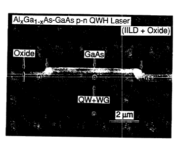
Figure 5 shows a cross section of the crystal
before removal of the Si02 masking layer. The vertical
arrows in Fig. 5(a) indicate, as labeled, the thicknesses of
the Si02 layer (left side) and of the native oxide layer (to
the right). Fig. 5(b) shows a cross section in which the
native oxide (right side) has been removed by etching in a
KOH-Y,3Fe(CN)~ mixture. The pair of vertical arrows in Fig.
~(v) indicates the location of the oxide prior to removal.
Figure 5 illustrates that the oxidation method of the present
WO 92/ 12536 - 3 3 - PC'T/US91 /04512
2~~~~~
.;.nveWicrti is somewhat sensitive to crystal orientation. For
example, reference to Fig. 5 shows i;:hat where the oxide
undercut the Si.02 masking stripe and the GaAs contact layer,
a tendency existod to develop a crystallographic step on the
AlyGal-xAs (where x was about 0.8) c:onfi.ning layer. This is
shown by the small slanted arrow in Fig. 5(b). This
sensitivity to crystal orientation :Lndicates that the native
oxide integrally conforms to the underlying crystal structure
which means that bonding problems at the interface would be
minimized or eliminated:
After the Si02 masking stripes were removed, the
crystal was sealed in an ampoule for. shallow Zn diffusion
(ZnAs source, 540°C; 25 min) to increase the GaAs stripe
contact doping. The crystal was them metallized with
titanium-platinurn-gold. (Ti-Pt-Au) across the native oxide
onto the exposed GaAs contact stripc-:. The metallization
adhered onto the native oxide much better than on oxides or
other dielectrics formed by prior art methods where the
metallization frequently peels. After the p-type side
ii~etaiiication, the crystal was thinned ( to 100 dun) from the
substra;.e side and was metallized on the n-type side with
germanium-gold-nickel-gold (Ge-Au-Ni.-Au). The wafer was then
cleaved into Fabry-Perot bars, saw-cut stripe-contact
sections were attached to copper heat sinks with indium (In)
for continuous wave (cw) laser operation at room temperature,
i.e., 300° K. Similar saw-cut sections with no contact
stripes were prepared in order to investigate the blocking
behavior of the o~:ide .
Figure 6ia) shows the current versus voltage (I-V)
c~~aracteristic of a diode prepared on the QWH crystal in the
GaAs contact stripe region; Fig. 6(b) shows (same scale) the
open-circuit diode that resulted when no contact strips was
WO 92/12536 ~ ' '1 PCT/US91/04512
present (i.t,., tle case of contact to a saw-cut section with
only the native o::ide on the crystal).
The high duality of those laser diodes was demon-
strated by their operating characteristics (continuous wave
at 300° K). The diodes (having a cavity approximately 500 dun
long) approached threshold, as shown in Fig. 7 by spectral
curves labeled (a) 20 mA, (b) 30 mA, and (c) 40 mA. The cor-
responding points on the power versus current (L-I) curve are
shown in the inset of Fig. 7. The power versus current char-
acteristics exhibited a rather sharp corner, reminiscent of a
distributed feedback or cleaved-coupled cavity diode. This
suggested that the oxide, unlike those formed by method of
the prior art, perhaps because of. its sensitivity to crystal
orientation, rippled or "milled" the crystal surface and
prcwided some natural distributed feedback. As the diode
approached threshold (Fig. 7) little tendency for multiple
mode operation (spectral "ringing") was shown. Spectral
curve (b) of Fig. 7 (30 mA) exhibited narrowing but no "ring-
ing", and just above threshold a single mode was dominant as
shown, in Fig. 7, at the higher current, (c) ~=0 mA.
Because of the quality of these recessed oxide
single-stripe diodes and the excellent adherence of the met-
allization on the natural oxide, they are easily attached
with indium to a copper heat sink on the oxide side, thus
providing very effective heat sinking in close proximity to
the QWH active region. Figure 8 shows the high power contin-
uous wave laser operation that was possible. The power out-
put per facet exceeded 100 mW before burn-out occurred.
Besides the high performance capability demon-
strated by the oxide-defined laser diodes of this Example,
one of their more notable features was their simple fabrica-
tion. Although a CVD SiOZ layer to mask to define the 10 um
W0 92/12536 -35' PCT/US91/045I2
wide GaAs contact stripes was employed, elimination of "his
step can be accomplished simply by photolithography, which
would make possible the fabrication of an oxide stripe laser
f ree of any CVD processes .
_.,._
PCT/US91 /04512
WO 92/12536
w.~~,r~nr r.
TTA'1'_tVE O~:IDI:;-DF,FINED rItTLTIPLE STRIPL
A1 Ga, T~.~~-GaAs pUANTUT~! WEhL HETEROSTRUCTURE LFSERS
t -~- ;
ns demonstrated in Example 2, ttoe more notable
faatures of the native AllGa1-xAs (x of about equal to or
greater than U.7) oxide that. forms in accordance with the
method of the present invention include how well it metal-
7.ized, (thus employable in device heat sinking), and how, via
ordinary photolithographic processes, the native o~:ide per-
mitted delineation of device geometries without the need t.o
deposit foreign anti potentially mismatched dielectric mater-
ials (such as, Si02 or Si.~N4). The present E::ample amplifies
these f eat.ures of the native ~~lXGa1-xAs ( x as def fined above )
oxide formed in accordance with the present invention by
constructing, with simplified processing, high performance
ten-stripe AlxGa~-XAs quantum-well heterostructure (QWH)
lasers. The considerable difference in the oxidation behav-
1 Or of A1 Ga., AS ( X Of a~7nt~t= a q~ta 1 t-O Or 7r oa tO.r t hail v . 7 )
X 1-X '
as compared to GaAs, which, relative to oxide formation, is
much weaker and readily permits current-contact metalliza-
tion, is shown.
The epitaxial layers for these coupled-stripe QWH
lasers were grown on n-type (100) GaAs substrates by metal-
organic chemical vapor deposition (MOCVD) as described in the
Dupuis, et al. reference cited in Example 1. A GaAs buffer
layer was grown first, followed by an n-type A10,8Ga0,~As
lower confining layer. The active region of the QWH was
grown next and consisted of a GaAs quantum well (QW) having a
thickness of about 400 R with A10,2JGa0,75As waveguide layers
(undoped; having a thickness of about 1000 ~) on either side.
W0 92/12536 -~7- PCT/US91/04512
~_,astly~, a: p-tY~?~ /;10. ~GaO. 2As upper confining layer was drown
to a t2u:i.ckness of about 9000 k on top of the active region.
The entire nWH was capped by a heavily doped p-type GaAs
contact layer about 80U A thick.
Tne GaAs contact layer was removed; where desired,
to provide access to the upper confining layer for conversion
of part of that layer to the native coxide by the method of
the present invention. The GaAs contact layer did not oxi-
dize readily, and consequently could be used directly as
mask (and them contact layer) when the native oxide formed
from a portion of the upper confining layer. Standard photo-
lithography was used to mask sets of ten GaAs stripes, 5 um
wide; located 2 pn apart (7 ~.m center-to-center spacing).
The GaAs between the stripes (2 um width), as well as the
GaAs between sets of stripes, was removed with H~S04:H?02:H20
11:8:80). This exposed the high composition AlxGal-xAs (x, of
about 0.8) upper confining layer to oxidation in accord with
the present invention. The gWH was heated at 400°C for 3
hours in an H20 vapor atmosphere obtained by passing N2 car-
rier gas (ha,Ji ng Q flow rate of about 1.4 scfh) through an
HBO bubbler maintained at 95°C.
The QWH crystal after oxidai:ion is shown in Fig.
9(a). The 5 wn GaAs contact stripes i:emained shiny (silvery)
and basically unaffected by the oxidat:ian. The remainder of
the crystal, including the 2 um regions between the GaAs
stripes, is covered with the native oxide tYrat formed by the
method of the present invention. The native oxide was clear
and transparent and uniform; it appeared blue in color be-
cause of optical effects and was 1000-1500 A thick. The
thickness of that portion of the upper confining that was
converted to native oxide was also about 1000 - 5000 A. Thus
the thickness of the native oxide was substantially the same
WO 92/12536 ° 38-- PCT/US91/04512
as or ~.oas than the corresponding thickness of the aluminum-
boar inc7 upper conf fining layer .
After the pWH was mctallized with titanium-plat.-
inum-gold (Ti-Pt-Au) by conventional techniques, across its
entire suz~facer it appeared as shown in Fig. 9(b). Before
metallization occurred, the crystal was Zn diffused (ZnAs2,
540°C, 25 rain) to a shallow depth to improve the contact on
the GaAs stripes. This procedure did not require and' special
mashing. The crystal was thinned to about 100 dun and was
metallized on the substrate side germanium-gold-nickel-gold
(Ge-Au-Ni-Au), and cleaved into Fabry-Perot resonator strips
that were t2ien saw-cut into separate 10-stripe dies. These
were attached to copper (Cu) using indium (In) on the stripe
side for heat sinl~>ing and electrical test. Died-~_ current
versus voltage (I-V) characteristics had low series resis-
tance (approximately 2 ohm, S2). This indicated that the GaAs
contact la~~er was not affected by exposure to the oxidation
method of the present invention. Additionally, the low leak-
age currents showed that the native oxide provided good cur-
l eii t i lOCkl.iicj .
The near-field and far-field radiation patterns of
one of these devices are shown in Fig. 10. The device was
mounted with the junction side upwards, and had a threshold
of about 95 mA cw. Fig. 10(a) shows the near-field image as
viewed with a Si metal oxide semiconductor (MOS) camera at a
continuous wave (cw) laser current of 100 mA. Eight of the
ten emitters of the array lased at this current. The other
two stripes were visible on a more sensitive scale, but could
not be shown without saturation of the camera by the eight
more intense emitters. The near-field image, Fig. 10(a),
demonstrates that effective current confinement is provided
by the native-oxide-defined stripes.
WO 92/12536 -39- PCT/US91/04512
icr. 1001 show:; the far-field pattern for the same
device used, for Fig. 10(a): The radiation was collimated
with a 25 mm f/0.95 lens and imaged on a l.~near charge-
c:oupled device array. The twin-lobe ;pattern shown is char-
acteristic of coupling with n-phase shift between emitters.
The lower trace of Fig. 10(:b) shows the far-field
pattern at 100 mA cw that corresponds to the near-field pat-
tern shown in Fig. 10(a). The left peak was dominant because
of non-~,zniforrn current injection and non-uniform operation
near the losing threshold. The peak ;separation of 6.8°
agrees with the calculated value of 6.9° for the 7um emitter
spacing (with a wavelength of 8470 A),. The full angle at
half-power (FAHP) of the left peak at 100 mA was 0,6°, which
indicates that coupling across the fu7:1 68 tun aperture of the
array (ten, 5 um wide stripes on 7 pn centers) occurred. At
higher currents, the carrier injection and the emitter inten-
sity were more uniform, resulting in t:he more balanced twin-
lobed far-field pattern shown at 145 mA in Fig. 10(b). Both
lobes of the top trace have a FAHP of 1.1°, indicating weaker
coupling of the 3rra~~ and; or coupling across a reduced aper-
ture of about 44 pn (7 emitters). The decreased peak separa-
tion of 5.0° indicates a slightly smaller phase shift between
emitters (the effect of transverse gain). An array of uncou-
pled 5-~.un wide emitters would have a far-field divergence
angle of 10° FAHP, roughly 10 times greater than the lobe
widths of the coupled array demonstrated here.
Because of the simple form of these coupled-stripe
lasers and how well they are heat sunk via the GaAs contact
stripes and the recessed native oxide, they were capable of
considerable power output before failure. The power versus
current behavior (continuous wave at 300° K) of one of the
diodes is shown in Fig. 11. The inset shows the output spec-
WO 92/12536 a s -40- PCT/US91/04512
crum at i0 mw (one facet), which shifted from 8456 ~, (i.466
V) to a dominant. mode at 8479 A (1.462 eV) at higher drive
currents and an output power of about 100 mw (single facet).
This corresponds to a temperature increase of about 10°C or
less, when there is significant bandfilling.
Inasmuch as the gain-guided lasers of this Example
couple over large distances, the emitter spacing can be fur-
ther increased and the heat sinking further improved. Fig.
12 shows the power versus current behavior of a 20-stripe
laser similar to that used in Fig. 11, but.,aith stripe separ-
ation increased to 5 um (see the Fig. 12 inset). Because of
power supply limitations, the laser operation was terminated
at 400 mw (single facet; 2 amp. A).
WO 92/12536 - 41- PCT/US91 /0451 2
r~: r ntnr r n
tJATIVE OXIDE MASY;ED IMPURITY--INDUCED LAYER
DI SORDERING OF A1 ,Ga ,As QUANTUM 4rTELL HETEROSTR'JCTURES
This example investigated the masking capability of
the native oxide tha forms on Al~Ga1_,XAs (X > 0.7) using the
present invention. In particular this. Example contrasted Zn
diffusion and impurity-induced layer disordering (IILD) be-
havior between a bare AlhGa1_xAs-GaAs superlattice (SL) or
quantum well heterostructure (QWH) crystal, and a SL or gWH
that was masked by a native oxide formed by the method of the
present invention. In the latter case (native oxide masked)
the quantum well (QW) and superlattice (SL) layers were shown
to be preserved.
The superlattice (SL) and quantum well heterostruc-
ture (QWH) crystals used in this Example were grown on (100)
GaAs substrates by metalorganic chemical vapor deposition
(MOCVD) as described in the Dupuis, et al, reference cited in
$xa.mpl a 1 , In the case of tile JL trryJr tal ( crystal ~ i ) , a
GaAs buffer layer was grown, followed by an undoped
A10.8Ga0,2As lower confining layer (the thickness of which
was approximately 0.1 dun) : Then the S:L, consisting of 40
GaAs wells (L" of about 110 A) and 41 ,~10.4Ga0,6As barriers
(LB of about 150 A), was grown. The total SL thickness was
approximately 1.05 tun. Lastly, a 1000 R A10,8Ga0.2As upper
confining layer was grown on top of the SL. The structure
was then capped with a 3000 A GaAs layer.
In the case of QWH crystal, i=he first part of the
MOCVD QWH (Crystal # 2) was an n-type GaAs buffer layer
(about 0.5 tun thick), which was followed by an n-type
A10.~5Ga0,75As intermediate layer. An n-type A10,8Ga0.2As
WO 92/12536 -42- PCT/US91/04512
209~g
lower confining layer was grown next. This was followedhy
flue pWli active region, which was a AlO,ObGaO.g~As (QW) quan-
t171i1 wE'l1 about 200 ~ thick, sandwiched by two undoped
A10 . Z,GaO , ~ JAs waveguide ( i~7G ) Layers of about 1000 n . Fin-
ally a p-type F,10.8Ga0,2As upper confining layer was grown to
a i_hickness of about 9000 h) on top of the active region.
The entire QWH, useful in laser diode construe+:.ion, was cap-
ped by a heavily doped p--type GaAs contact layer havinq_ a
thickness of about 800 A.
The GaAs cap layer. on both the SL and the QWH, was
removed to expose the upper AIGaAs confining layer (x of
about 0.8) to the oxidization method of the present inven-
tion. The presence of Ga in the oxidized layer ar_d at the
native oxide-semiconductor interface did not adversely affect
the structure of the native oxide that formed because the
oxygenated gallium and aluminum compounds form structural
isomorphs having similar crystalline form, and A1203 and
Ga2oj form a solid solution over the entire compositional
range represented by the upper confining layers of the SL and
,.. ,.
vwri. The A~xGal-XAS nxirl~tiCn ;~;uS gC.:.Cmpii,Sh ed iii c'tCl:vrCl
with the present invention by heating the samples at 400°C
for 3 hours in an ii20 vapor atmosphere obtained by passing N2
carrier gas (with a flow rate of about 1.5 scfh) through an
H20 bubbler rna.intained at 95°C.
In order to effect selective Zn diffusion and layer
disordering in the SL sample (Crystal #1), a photoresist
stripe pattern (20 um stripes on 50 um centers) was defined
on top of the native oxide thus formed. Using a NH4F:HF
(7:1) buffered HF solution, the native oxide was selectively
removed in a stripe pattern, as shown in Fig. 13. The sample
was then cleaned in an NF~40H solution and immediately sealed
in an ampoule with a piece of ZnAs2 (lU mg) for the Zn diffu-
WO 92/12536 ~ '1'1
,11CT/US91 /04512
lion (at eU0°C for i hour). A shallow-angle lap of th~~ SL
sample after the diffusion is shown in: Fig. 13. The native
oid~ mask, formed in accord with the practice of the present
invention, which is indicated by the downward arrow labelled
"oy.ide" in Fig. 13, masked the underlying A10.4Ga0.6As-GaAs
SL from the diffusion of Zn, and from layer intermixing that
occurred in areas where the oxide had been removed. The 40
period SL (having a total thickness of about 1:05 um) was
seen to be clearly intact ber~eat.h the native oxide mask,
while intermixed elsewhere.
In the case of the QWH wafer (Crystal #2), two
sample; were sealed in an ampoule with ZnAs2 for simultaneous
heating and for IILD diffusion (at 5?5°C for l hour). One
sample had a native oxide maskina layer on it as formed by
the method of the present invent~.on, while the other sample
was the QWH with simply the GaAs cap layer removed. Similar
to the selective Zn-IILD of the SL of Fig. 13, the QWH sample
having the oxide as formed according to the present inven-
tion, did not disorder. In comparison, layer intermixing
occurred for tllP QWT_j Onmpari_cn_n_ g~~,n~ a :~:hiCh d' ~
r~ .i.~. nw iauvc we
native oxide masking layer on it; (as determined shown by
photoluminescence measurements).
The QWH samples, both masked and not-masked, were
prepared for photoluminescence measurements by first lapping
and polishing the crystals, using conventional techniques, to
a thickness of approximately 2 mils. tJext, the remaining
substrate and GaAs buffer material were removed by wet chemi-
cal etching in H2S04:H202:H20 (4:1:1), followed by selective
etching. A photomicrograph of an oxidE~-masked portion of the
QWH (Crystal #2) is shown in Fig. 14. The photomicrograph of
Fig. 14 was taken with light that was transmitted through the
thinned QWH crystal at a spot which wa~~ "rough etched" all
WO 92/12536 - 4 4 PCT/US91 /04512
cI-rc: way to the oxide layer, thus revealing features or the
QWH and o.f th~~ rrati ve oxide that was produced Ly . the me thod
of the L>resent invention .
RefCL'I'ing to Fic~. 14, Region A of the photomicro-
graph showed the native oxide to be of excellent quality,
i.c., it was clear and transparent and similar to the oxide
that was produced in the oxidation of l:he AlAs-GaAs SL cry-
stals of Example 1. Indeed, the oxide was so clear that
specks of dirt on thr~ surface of the oxide were easily seen.
~'ho remaining regions showed the various layers of the QWH
material deeper into the crystal. At Region B, the oxide
plus the upper QWH confining layer (AlO.~Ga0.2As) were seen
and were yellow in color, due to optical effects. In Regio:.
C, the waveguide plus the QW active region, as well as the
upper and lower confining layers, were seen as or4nge in
color, also due to optical effects. Finally, in Region D,
the entire thickness of the QWH was seen as red in color
(again due to optical effects). Some of the buffer layer
(where X was about 0.25) that was not completely removed at
t~"1!~ f_'YlIC'f'.~l edgy ;~;u~ ul.Sv jGeit Zn IlegZOn D.
To further examine the capability of the native
oxide that is produced by the present invention to mask the
crystal from Zn-IILD, cleaved samples were examined via
photoluminescence (PL). Native-oxide masked and non-masked
samples that had been exposed simultaneously to the Zn and As
ambient at 5?~°C for 1 hour (the Zn-IILD) were heat sunk in
copper under diamond for photopumping with an Are laser (5145
A). The resultant photoluminescence spectra (laser opera-
tiore) are shown in Fig. 15.
Fig. 15(x) shows that the lasing wavelength (con-
tinuous operation, 300° K) for the native-oxide-masked sam-
ples occurred at 7992 A (1.565 eV); while that for the pulse-
W0 92/ 12536 - 4 5 - PCT/US9l /04512
oxcited non-masked comparison samples, Fig. 15(b) was shifted
to 7140 R (1.736 eV). The shift of approximately 170 meV in
the: laser operation of the non-masked gWH crys al (Zn-ILLD),
Fig . 15 ( b ) , agreed with what was expected f or a Aly Ga.l -};As QW
(x of ak~out 0.06) intermixed into a bulk-crystal waveguide
region (x of about 0.25). This indicated that the non-masl~:ed
samples had been intermixed ;(with an energy shift of about
170 meV), while the native-oyide-masked samples, Fig. 15(a),
were intact. Also, for the Fig. 15(a) samples, QW band-fill-
ing was evident, while for the IILD Fig. 15(b) samples, only
x~ulk-crystal behavior was evident. Interestingly, photoexci-
tation of the native-oxide-masked (a) samples of Fig, l5(a)
t~or, place through the transparent oxide, indicating that the
native oxide, formed by the present method was of high qual-
ity.
WO 92/12536 ~ - '~ b - PCT/US91 /04512
i~XAT~1PLE
LOW-'THRESHOLD DISORDER-DEFINED 2dATIVE-OXIDE-DELINEATED
BURIED-FiETEROSTRUCTURE A1 Ga As-GaAs QttANTUI~g WELL LASERS
Impurity-induced layer disordering (IILD), such as
described by W. D. Laidig, et al. in Appl Phys. Lett., _38,
776 (1981) and D. G. Deppe, et al. in J. Appl. Phys., 64,
F.93, (1988), has been employed to produce very high per-
formance planar buried-heterostructure (BH) quantum well
heterostructure (QWi3) lasers such as described by D. G.
Deppe, et al. in J. Appl. Phys., 58, 4515 (1985). Various
dopants and diffusion techniques have been employed to fabri-
cate disorder-defined BH lasers, including: (1) Si solid-
sourc~ diffusion, (2) Si implantation and annealing, (3) Ge
diffusion from the vapor, (4) Zn diffusion from the vapor,
(5) Si-O diffusion from A1-reduced Si02, (6) Si diffusion
from Al-reduced Si/Si3N4 via rapid-thermal annealing, and (7)
Si diffusion from laser melted Si.~t~4. Many of these diffu-
sion sources and tecnniq~~es s~,~f~~Y ;r ~-h =_, ,_
1 \.1 11 c»~ ~~ a ~ d~ t tmaL they
form a very highly conductive layer at the crystal surface,
possibly due to the formation of a dopant-crystal alloy.
This conducting layer is a source of leakage, thus increasing
laser threshold currents. Indeed, under certain conditions,
the dopant-crystal alloying i~ so severe that a relatively
deep proton implant is required to passivate the leakage
regions and ensure low threshold operation.
This Example demonstrates a "self-aligned" process,
in which the crystal surfaces were converted to a high-
quality, current-blocking native oxide by the method of the
instant invention. The oxide thus formed was found to passi-
vate the surface, thus reducing leakage currents and yielding
WO 92/12536 7 PCT/US91/04512
an improved form of low thre hold disorder--defined BH
AlxGa1-xAs-GaAs quantum well heterostructure laser.
The QWH laser crystal employed in this Example was
grown by metalor.ganic chemical vapor deposition (MOCVD), as
described in the Dupuis, et. al. reference cited in Example 1,
on an n-typo substrate. The growth b~_gan with n-type buffer
layers of GaAs having a thickness of about 0.5 um and
Alp , 25Ga0 , 75As having a. thickness of <~bout 1 dun. This was
followed by the growth of: an approximately 1.1 um thick
A10.77Ga0.23As n-type lower confining layer; an approximately
2000 R thick A1p,25Ga0.7~As undo~ed waveguide region; an ap-
proximately l.1 um (11,600 P~) thick A10.8Gap,2As p-type upper
confining layer; and an approximately 0.1 pn thick p-type
GaAs cap. In the center of the waveguide, a A10.06Ga0.94As
quantum well, undoped, having a thickness of about 20U R was
grown.
The laser diode fabrication process began with a
shallow Zn diffusion over the entire surface, in an evacuated
quartz ampoule at 540°C for 30 min. The shallow p+ layer
;ormAd by the diff~,aicr. helped control. iaterai Si diffusion
at the crystal surface (under the masls:ed regions) in later
processing steps. After Zn diffusion, the crystal was encap-
sulated wi h about 1000 A of Si3NQ which was deposited by
conventional chemical vapor deposition (CVD) at 720°C. The
Si3N4 was patterned with photoresist a.nd etched with a CF4
plasma into two stripe widths: 4 pn a.nd 6 um: The photo-
resist was removed, with the remaining Si3N~ stripes serving
as masks during chemical-etching, with H2S04:H202:H20
(1:8:80), of the GaAs contact layer. This etching left the
high-gap A10,8Ga0.2As upper confining layer exposed. Follow-
ing stripe delineation, CVD techniques were used to deposit
an approximately 300 A thick Si layer (CVD at 550°C) and an
W0 92/ 12536 - ' 8 - PCT/US91 /04512
approximately 1700 A thick Si02 cap layer (CVD at 400°C).
The crystal was the~t'.sealed in an evacuated quartz ampoule
and annealed with excess As at 850°C for 6.5 hours. The high
temperature anneal resulted in Si diffusion and IILD outside
o.f the GaAs contact stripes.
The encapsulant was removed by etching with a CF4
plasma, and the crystal was oxidized according to the present
invention as follows: The crystal was placed in an open-tube
furnace (supplied with a N2 carrier gas bubbled through HZO
at 95°C) at 400°C for 3 hours. This resulted in the conver-
sion of approximately 2000 A of the exposed upper confining
layer at the edge and beyond the GaAs contact stripe regions.
The thickness of oxide layer formed was s~.tbstantially the
same as the thic?mess of tha t portion of the upper conf fining
layer that was converted. No oxide was formed on the GaAs
contact stripes due to the selectively of the oxidation pro-
cess. The formation of native oxide only in areas of high
aluminum composition resulted in contact stripes that were
seJ.f-aligned. Following oxidation by the method of the in-
vention, the wafer was sealed in a.~. a.Tp~vuic wit h d GilA~2
source, and was annealed at 540°C for 30 min to form, only in
the contact areas, a shallow, heavily doped p-type region.
Samples were then conventionally lapped to a thickness of
about 5 mils, polished, metallized with titanium-gold (Ti-Au)
on the p-type side, metallized with germanium-nickel-gold
(Ge-Ni-Au) on the n-type side; the samples were then cleaved
into bars approximately 250 lun in length.
Figure 16 shows a scanning electron microscope
SF.M) image of a stained cross section of a 6-Wn-stripe BH
laser structure after the Si-IILD and the oxidation method
of the present invention that resulted in self-aligned con-
tact stripes. Reference to Figure 16 shows that the impur-
WO 92/ 12536 - 4 9 - PCT/US91 /04512
2~r~~~8~
qty-induced layer disordering intermixed the waveguide region
with the surrounding confining layers (autside of the GaAs
contact region) and provided current ~,~.onfining p-n junctions.
Lateral diffusion resulted in a contact region of appro;:i-
mately 5.5 dun and an active region having a width of approxi-
mately 7 um. Similarly, for diodes processed with 4 l.~m
stripes, the contact region was about 2..5 l.un with an approxi-
mately 3pn wide active region. Oxidation by the method of
the present invention, of'the high-gap AlxGalOxAs regions
outside of the GaAs contact stripe resulted in the formation
of a high-quality current-blocking native oxide at the cry-
stal surface. The oxide grew all the way to the edge of the
GaAs contact stripe, a indicated in F'ig. 16 by the unmarked
vertical arrows at the "notch" at the stripe edges. This
resulted in the self-aligned passivation of areas having the
potential for leakage by conversion of these areas to the
native.oxide. The native oxide was actually thicker than it
appeared in Fig. l6 since the stain, Y,3Fe(CN)6-KOH, that was
employed to resolve the heterolayers also etched the oxide.
Th°_ laser diodes fabricated using native oxide as
formed by the present invention typically exhibited pulsed
thresholds between 3.5 mA and 6 mA (for the 3 pn stripe) and
7.5 and 9.5 mA (for the 7 ~ stripe), ,as tested in a probe
station. Figure 27 shows the continuous wave (cw) light
power versus current (L-I) curve of a :3 Wn stri.pe diode that
was mounted p-side down on an indium-coated (In-coated) cop-
per (Cu) heatsink. The room temperature (300° K) continuous
wave (cw)) threshold was 5 mA for this device (uncoated fac-
ets). Spectral data indicated that the: diode first began to
narrow spectrally and "ring" at about ~~ mA, which accords
. with good carrier and optical confinement and low edge leak
age. Lasing occurred at $198 R, with single-longitudinal
WO 92/ 12536 ~~ 5~ ~~ PCT/LJS91 /04512
_..
node operat.i.~n well developed at ? mA and extending up to at
least 20 mA. The laser diode exhibited an external differen-
tial quantum efficiency of 53~ (up to about 10 mW) and an
output power of greater than 31 mW/facet before catastrophic
damage occurred. At powers e~reater than 10 mW, the increas-
ing curvature of the L-I plot indicated that heating effects
becarne significant. However, this phenomenon was due to the
relatively high forward resistance of the diodes (R~ of about
20R), and not. to the inability of the native oxide to dissi-
pate heat. Thus the native oxide formed by the method of the
instant invention acted as an excellent current-bloc);ing
layer for stripe-geometry laser diode operation. These
diodes exhibited sharp turn-ons and no observable leakage
through the oxide. '
Unmounted, the laser diode of Fig. 17 exhibited a
pulsed threshold of 4.5 mA. Other diodes also exhibited a
very small increase (usually less than 0.5 mA) in pulsed
(unmounted) versus continuous wave (mounted) laser thres-
holds. These increases were much smaller than those typic-
ally observed for other fabrication processes. This was
attributed to better thermal contact between the metalliza-
tion and the oxide formed by the invention, as well as better
oxide heat conduction, over that for other masking encap-
sulants. In addition, the formation of the native oxide by
the invention "consumed" the highly doped surface layer.
Thus, the high-gap shunt junctions had lower doping, and thus
lower capacitance. Compared to continuous wave operation,
high shunt junction capacitance causes the leading edge of a
pulsed current to divide differently between the quantum well
junction and the shunt IILD junction, which leads to a sig-
nificant difference in pulsed versus continuous wave laser
thresholds. Thus diodes with lower shunt capacitances will
WO 92/12536 - ~' ~ - '~ ~ ~ ~ ~ PCT/US91/04512
hrive more similar pulsed and continuous wave laser thresholds
than those with high capacitances.
The ~:ield pattern:: of a 3-u,m stripe laser are shown
in Fig. 18 for continuous wave operation at 12 mA. The tiear-
field pattern, Fig. 18(a), had a full width at half maximum
of about 3.~u,m, which agreed closely with an active region
having a width of about 3 um, as observed in SEM micrographs.
The far-field pattern, Fig. 18(b) had a full angle at half
maximum of about 20 . 4 ° , wh.ich corresponded to the dif f racoon
limited operation of a 3 um stripe.
W0 92/ 12536 ' 2 PCT/US91 /04512
EXAi~IPLE 6
Np.TIVE OXIDE STAF3ILIZATION
OF AlAs-GaAs HETEROSTRUCTURES
This Example compares the high quality and stabil-
izing nature of the native oxide formed in accordance with
the present invention with the inferior quality and destruc-
tive nature of oxides that form at temperatures lower than
that prescribed in the practice of the instant invention. In
particular, this Example compares the quality of the native
oxide that forms on ex>posure to water vapor and nitrogen gas
and a temperature of 400°C after 3 hours, with the oxides)
that form by exposure to atmospheric moisture and tempera-
ture, which conditions are representative of oxide formation
under a temperature of 375°C.
The crystals used in this experiment were grown by
metalorganic chemical vapor deposition (MOCVD) on (100) n-
type GaAs substrates in an EMCORE GS 3000 DFM reactor at
760°C. The crysta_1 gro~~tr prossurc, Group V/Grc~up iii ratio,
and growth rate were 100 Torr, 60, and about 1000 A/min,
respectively. An undoped GaAs layer approximately 0.5 dun
thick was grown first, followed by an nominally undoped AlAs
layer about 0.1 iun thick. The crystal was then cleaved in
two. One half of the cleaved crystal was exposed to atmos-
pheric conditions at room temperature (Sample a). The other
half was oxidized, according to the method of the present
invention, at a temperature of 400°C for 3 hours in an H20
vapor atmosphere obtained by passing N2 carrier gas (having a
flow rate of about 1.5 scfh) through an H20 bubbler main-
tained at 95°C (Sample b). Sample (b) was then exposed to
atmospheric conditions identical to those for Sample (a).
i;
WO 92/ 12536 - ~' ~ - PCT/US91 /04512
,,2~W6~ . .
within hours after exposure, the Sample (a) crystal
began to degrade in color to a yellowish brown, while the
Sample (b) crystal maintained a uniform blue: appearance (the
oxide was clear and transparent, the blue color was a result
of optical effects). Figure l9 is a t~lomarski image photo-
graph of the surfaces of crystal Samp:Les (a) and (b) after,
in both cases, atmospheric exposure for 100 days. The sur-
face of Sample (a) was clearly "rougher" than that of Sample
(b). Several days after the 100 day aging process, Sample
(a) showed si_qns of nonuniformity around the edges of the
crystal, while Sample (b) remained unchanged. The oxidized
surface of Sample (b) was smoother than the surface of Sample
(a), and the cleaved edge of Sample (b) was intact whereas
the edge of Sample (a) showed signs of destructive attack (as
indicated by roughening).
Figure 20 is a scanning electron microscope (SEM)
image of the edges of Samples (a) and (b): The edges were
unstained, cleaved cross sections that had been aged 100
days. Sample (a) showed signs of chemical attack into the
Crystal. WhlCh dE'_pt~'1 waS well beyond thL' 3pproiii~?~atel;y U.1 /1m
thick AlAs top layer of the As-grown crystal. In contrast,
the cross section of the Sample (b) exhibited a native oxide
layer that was substantially the same thickness as the AlAs
top layer of the As-grown crystal, the thickness of the na-
tive oxide being approximately 0.1 dun thick; the native oxide
also showed no perceptible sign of degradation. The cross
section of Sample (a) also appeared to be nonuniformly
etched. This was surprising in that the sample was not
stained to high-light this layer.
The results of secondary ion mass spectrometer
(SIMS) analysis on Samples (a) and (b) talten after 80 days
are shown in Fig. 21. Both Samples (a;l and (b) had large
_ .- . _
WO 92/12536 ~~ t PCT/US91/04512
~~ ~ ,
oxygen and hydrogen signals (indicated by J,l-O-H ion count)
ire the top 0.1 lun of thickness. I~lore unusual was that Sample
(a) showed a significant Al-O-H ion count as deep as about
1.0 um intc., the crystal itself. This was in sharp contrast
to the A1-U-H signal in the Sample (b), where the ion count
for A1-O-H decreased steadily after approximately the first
0.1 um of thickness, which represents the layer formed by the
native oxide. The A1-U ion count tracked the x.l-O-H signal
in bath samples. Another striking difference in the two
crystals was the Ga depletion that was evident in the top 1
~.m of Sample (a), which indicated that chemical reactions and
degradation of the crystal was occurring. The Ga signal of
Sa,~nple (a) increased at the AlAs-GaAs interface, that is, at
approximately 0.1 dun, and then decreased again at the sur-
face; however, no such "spike" in the Ga signal was observed
in the case of the Sample (b) and Sample (b) did not show
signs of any such chemical reactions or degradation; these
results are in accord with the SEM images of Fig. 20 and
demonstrate that the native oxide that formed from approxi-
mately the first 0.1 Wn of Sample (b) by tho rnoth~d of the
3
present invention was stabilizing in nature.
SIMS analysis also showed a dip in tire Al-O-H
signal in about the first 0.1 Iun of Sample (b) which dip was
not present in Sample (a). Transmission electron microscope
images of similarly oxidized heterostructures indicated that
there was a slight contraction of the native oxide layer to
roughly 60o to 700 of original thickness of the AlAs tap
layer. This contraction can be explained by the fact that
the molar volume of AlO(OH), which is one of the possible
products of an A1-H20 reaction, and does not deleteriously
effect oxide quality when present in modest quantities, is
270 less than the molar volume of AlAs. (The molar volumes
CA 02099385 2001-O1-24
WO 92/ 12536 ~' S 5" PCT/US91 /04512
of the anhydrous; a and phases of A12U3 are approximately
oqual to that of AlAs which indicates formation of one or
bath probably a-A1?O, as a major component of the native
oxide of the instant invention). The contraction of the AlAs
layer to about 0. 06 Wn to 0 . 0-I dun ( as indicated by the dip in
the T.1-O-H signal) suggests that A10(OH) is either an inter-
m~diate or, less likely, an end product of the oxidation
method of the presen'~ invention. I~lore likely, the contrac-
tlUll lIl thicYness is caused by the loss of arsenic. Several
reactions involved in the AlAs oxidation are possible:
AlAs + 3Y.20-~ A1 ( OH ) 3 + AsH3 ~ ( 1 )
AlAs i 2H20-~.3A10(OH) + AsH3 '~ (2)
;Alms + 3H20 -~ Al?03 + 2AsH~ ~ (3)
Reactions involving the formation of As20.1 are also possible
but are less likely given the extent of As depletion (as
shown in Fig. 21) in the AlAs layers in both the Samples (a)
and (b).
Reaction (1) probably occurs in Sample (a) and is
likely responsible for the inferior quality of the oxides)
produced; the standard heat of formation of A1(OH)3 being
greater than that of either a-A1203, ~ -Al2o.~ or A10(OH) at
300°1:. This is also in agreement with the phase diagrams
showing the most thermodynamically stable phase at 300°K
under atmospheric pressure. See, E. M. Levin, et al. Phase
Diagrams For Ceramists (The American Ceramics Society, Colum-
bus, Ohio) Fig. 2008, P. 551 (1964); Fig. 1927, P. 527 (1964)
and Fig. 4984, P. 426 (1975).
The As depletion that occurs in roughly the first
0.1 um of Sample (b), as shown in Fig. 21, was two orders of
CA 02099385 2001-O1-24
WO 92/ 12536 - ' ~ - PCT/US91 /04512
magnitude greater than that for Sample (a). This suggests
ll~at a second reaction irf the AlAs layer of Sample (b) takes
pl.acA which liberates still more As (as the volatile product
A~fl3) thus increasing contraction of the native oxide layer.
The possible reaction may be:
A10(OH) + AlAs + H20 -~ A1203 + AsH3 '~' (4)
The greater As depletion in the AlAs layer of Sample (b), as
cotnpared to Sample (a), indicates that As may play a signif-
icant role in the formation of the stable native oxide of the
invention and may, in fact, catalyze the reaction of hydroxyl
(OH ) groups in AlAs. The presence of hydroxyl groups are
thought to be responsible for the instability of the oxides
of Sample (a) and for the inadequacies of oxides from prior
art thermal oxidation techniques.
As to oxygenated gallium compounds, gallium tri-
hydroxide, Ga(OH).~, is the most likely Ga-O-H compound formed
at room temperature and atmospheric pressure. Gallium hy-
droxyoxicie, Ga0(OH), is the most likely form at about 100°C
and gallium oxide, a-Ga203, the stablest form, at about
400°C. Both Ga(OH)3 and Ga0(OH) have inadequate physicality
for semiconductor purposes and also would cause an expansion
in oxide thickness when present. It is believed that Ga(OH)3
and Ga0(OHj are formed at temperatures under the 375°C pre-
scribed by the practice of the present invention and thus
would likely be formed in undesirable quantities by thermal
oxidation techniques of the prior art. Because Ga(OH)3 is a
much stronger acid than is A1(OH)3, A1(OH)3 being amphipro-
tic, there is also a strong likelihood that a reaction be-
tween these two hydroxides occurs thus further exacerbating
the deleterious effects these materials have on semiconductor
structure. Since (when in hydrous form) both are also elec-
WO 92/12536 r~7 PCT/US91/04512
trc~lytos, the presence of light may contribute to the re-
action .
~dh;lc~ there are indications that Ga-O-H and AI-O-H
compounds are also present in the native oxide of the present
invention it is clear that even if prE:sent, they did not at-
tach tree crystal of Samplo (b) as in t:he case of the Sample
la). The reduction of these particular hydroxides at higher
temperatures used in forming the native oxide of the present
invention (at greater than about 375°C:), apparently stabil-
izes the A1-H2o and Ga-H20 reactions; thus inhibiting the
destructive chemical reactions attendant lower temperature
oxidation.
WO 92/12536 -S~' PCT/US91/04512
T~Y1~.~.TT~T L' '1
FATE OF r:ATTVE OXIDi~'~', FORI~'IATION B'.~' RAPID THERIdAL PROCESSING
J'. f urnance at 650°C was ~;rovicied with a water vapor
environment obtained by passing N2 gas through an H20 bubbler
at 95° w 10~°C; nitrogen gas flow rate was appro~;imately 1.9
scfh.
Zn order to minimize thermal mass effects, the
quartz boat used to carry the samples of this example
remained in the furnace until the samples were ready to be
oxidized. The samples utilized were a crystal having an
AlvGa1'Yt,s layer, where x was between about 0.8 to about 0.9.
To oxidize the crystals, the quartz boat was
removed from the furnace and a sample was loaded onto the
boat. The sample and boat were then placed into the furnace.
Oxidation time periods of between about 15 seconds to about
l0 minutes were employed for separate samples. At the end of
each oxidation the sample used was quickly removed from the
fur nace .
For each sample, the rate of native oxide formation
was observed to be about 0.1 Iun (about 1000 A? of native
oxide formed for about every 15 seconds of oxidation time
using the rapid thermal processing of the present invention.
W0 92/ 12536 "' 9 - PCT/US91 /04512
_-.~~w,T r. ~t
ItJDEX OF REFR/~CTION MEASUREMENTS
A native oxide layer was formed from four samples
of A10,8Ga0.lAs (each such layer was about 0.4 um thick)
overlaid on a GaAs substrate. The samples, Samples l-4, each
had a GaAs cap (about 0.1 ~.un thick) which was removed with an
~I2SOQ:H202:H20 (1:8:80) solution; the samples were
immediately oxidized in accordance with the procedure used in
Example 7. Oxidation times for Samples 1-4 were 1, 2, 4 and
minutes, respectively.
Eliipsometer measurements, using conventional
equipment and a wavelength of ~~ = 632'r3 R, determined the
thicl~:ness and index of refraction of 'the oxide layers thus
formed in accordance with the present invention. The results
are shown in Table 2, below:
TABLE ?.
Oxidation Index of
Sample Time (min. Thickness (dun) Refraction (n)
)
1 1 0.38 1.57
2 ?. 0.41 1.54
3 4 0.39 1.55
4 10* -- --
* Data for the 10 minute oxidation time are not
presented due to significant scattering of the probe beam
which reduced the accuracy of t2ne measurements.
WO 92/12536 ~ ~ ~ ~ f ~ PCT/L,'S91/04512
As aYpar<°nt from Table 2, the Alp~~Gap.lAs layers
Samples 1-3 were ~substanti.ally completely oxidized and that.
the thickness of the resulting native oxides were
:substantially the same as or less than the thicl~:ness of the
Al~~BGa~~.iAs layers that converted. The indices of
rc.f.raction of the native oxides thus formed ranged from 1.54
- 1.57, which indicated that the native oxide thus formed on
each sample was formed primarily of dehydrated aluminum
compounds .