Note: Descriptions are shown in the official language in which they were submitted.
,a99~r~
PRINTED CIRCUIT BOARD
TECHNICAL FIELD
The present invention relates to a printed circuit board for
electrically interconnecting electronic components, the printed circuit
board being either flexible or non flexible.
BACKGROUND ART
Flexible printed circuit boards embedding parallel conductive
wires therein are widely used throughout the electronics industry ~-
particularly in applications for interconnecting electronic modules on
which electronic components are mounted in high density. The
15 application of a ribbon cable assembly to electronic equipment drawers is
disclosed in United States Patent No. 4,660,125 issued to Purdy et al. on
April 21,1987. The ribbon cable assembly is flexible so as to allow
interconnection of a cabinet and a slidable drawer in which circuit cards of
electronic components are mounted. However, the standard ribbon cable
20 assembly has no electric and magnetic shielding.
To provide electric and magnetic shields, flexible printed circuit
boards in which parallel conductive wires are sandwiched between a mesh,
have been proposed. In telecommunication applications, these conductive
wires include pairs of tip and ring conductive wires for telephone lines.
25 The conductive wires interconnect components to transmit electric signals
between components. In known flexible printed circuit boards, the
conductors forrning the mesh generally intersect each other at right angles,
and the longitudinal axes of the tip and ring conductive wires are oriented
to run parallel to the intersections of the mesh. In such an arrangement, it
30 is difficult to control placement of the parallel conductive wires relative to
the intersections of the mesh. As a result, one conductive wire may be
closer to the intersections of the conductors of the mesh than the other
conductive wire. Should this happen, the capacitance between that one
conductive wire and the mesh will be greater than the capacitance between
2 a 5 ~ ~ ~ 7
the other conductive wire and the mesh. Due to this unbalance, higher
levels of cross talk are unavoidable, particularly between adjacent pairs of
conductive wires transmitting signals. At audio frequencies, this was not a
serious problem. However, at the very high frequencies and bit rates now
5 being transmitted, this unbalance has become a critical problem.
': : ,
SUMMARY OF THE INVENTION
It is an object of the present invention to provide an improved
10 printed circuit board.
According to the most general aspect, the present invention
provides a printed circuit board for electrically interconnecting electronic
components, comprises: a non-conductive supporting member; a
conductive mesh supported by the supporting member, the mesh defining
15 an array of intersecting conductors; and at least one pair of parallel
conductive wires supported by the supporting member equidistant from
the conductive mesh. In the printed circuit board, the longitudinal axes of
the pair of conductive wires are oriented at an angle relative to
intersections of the conductors of the mesh, so that the offset of the
20 intersections from the conductive wires incrementally changes along the
longitudinal axes of the pair of conductive wires so that the capacitances
between the conductive wires and the mesh are substantially balanced
regardless of the lateral position of the wires.
In such an arrangement of the conductive wires and the mesh,
25 the capacitance between the one conductive wire and the mesh will be
substantially equal to the capacitance between the other conductive wire
and the mesh. Due to this substantial balance of the capacitances, low cross
talk between adjacent pairs of parallel conductive wires transmitting
signals is ensured.
In a preferred embodiment, the non-conductive supporting
member is a flexible non-conductive one and the printed circuit board
includes a further conductive mesh defining an array of intersecting
conductors supported by the sheet, parallel to the one conductive mesh. In
' .
, " ,"
2~9~77
this printed circuit board, the parallel conductive wires are sandwiched
between and equidistant from both of the meshes. The longitudinal axes
of the pair of conductive wires are oriented at an angle relative to
intersections of the conductors of both of the meshes. The conductors of
5 the one conductive mesh are substantially parallel to those of the further
conductive mesh; and the pitch of the intersections of both of the
conductive meshes is substantially identical. Also, in a preferred
embodiment, the angle between the longitudinal axes of the pair of
conductive wires and the longitudinal axes in the direction of the
lo intersections of the conductors of the mesh is about 7. Such an angle
provides good flexibility of the printed circuit board and balanced
capacitance regardless of the lateral position of the pair of conductive wires.
As well, with the two conductive meshes sandwiching the parallel
conductive wires, ideal electric and magnetic shielding is provided.
BRIEF DESCRIPTION OF THE DRAWINGS
Embodiments of the present invention will now be described by
way of example only with reference to the accompanying drawings in
which:
Figure 1 is a plan and partially broken view of the printed
circuit board according to the present invention;
Figure 2 is an enlarged vertically sectional view of the printed
circuit board on line II-II in Figure 1;
Figure 3 is a sectional view of the printed circuit board on line
III-III in Figure 2;
Figure 4 is an enlarged vertically sectional view of another
printed circuit board according to the present invention;
Figure 5 is an enlarged vertically sectional view of another
30 printed circuit board according to the present invention; and
Figure 6 illustrates another ground conductive mesh which is
used for the printed circuit board according to the present invention.
2 Q 9 ~
BEST MODE FOR CARRYING OUT THE INVENTION
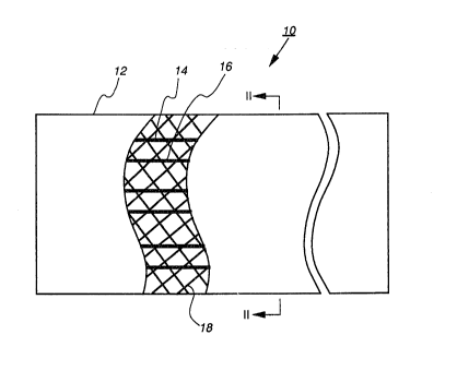
Referring to Figures 1-3, a flexible printed circuit board 10
comprises a flexible non-conductive sheet 12, a plurality of pairs of tip (T)
5 and ring (R) conductive wires 14 and 16 and a pair of conductive meshes 18
and 20 which each form a ground plane. The tip and ring conductive wires
14 and 16 which run in parallel are supported by the flexible non-
conductive sheet 12 and are equidistant from the two meshes 18 and 20.
Typically, the conductive wires 14 and 16 are of copper, and the width of
10 the conductive wires 14 and 16 is 0.010 inches and the distance S between
the two wires is 0.025 inches.
The meshes 18 and 20 have a plurality of conductors 22 and 24,
respectively. The conductors 22 of the mesh 18 and the conductors 24 of
the mesh 20 are both embedded in the flexible non-conductive sheet 12.
5 Each of the conductors 22 and 24 forms a matrix, defining an array of
intersecting conductors. The pitch of the intersections of both conductors
22 and 24 is identical and thus, the matrix of both meshes 18 and 20 is also
identical. The conductors 22 are overlaid the conductors 24. Typically, the
width of the conductors 22 of the mesh 18 (or the conductor 24 of the mesh
20 20) is 0.008 inches and the distance D between the conductors 22 (or the
conductor 24) is 0.040 inches.
The conductors 22 of the mesh 18 (or the conductors 24 of the
mesh 20) run substantially at right angles to each other. The longitudinal
axes of the tip and ring conductive wires 14 and 16 are oriented at an offset
25 angle 0 related to a phantom line 26, which is one running through the
intersections of the conductors 22 of the mesh 18 or the conductors 24 of
the mesh 20, as shown in Figure 3. The offset angle 0 is preferably quite
small to optimize flexibility of the printed circuit board 10. In the present
example, the chosen offset angle 0 is 7. Accordingly, with orientation of
30 the longitudinal axes of the tip and ring conductive wires 14 and 16 at the -
offset angle 0 (= 7), the offset of the intersections from the conductive
wires 14 and 16 incrementally changes along the longitudinal axes of the
conductive wires. In such an arrangement of the tip and ring conductive
........ ~ .. ... ... -.. ....
2~9~77
wires 14 and 16 and the meshes 18 and 20, both conductive wires 14 and 16
of one pair will, over an extended length, evenly cross the intersections of
the conductors 22 of the mesh 18 and the conductors 24 of the mesh 20
regardless of the lateral position of the wires 14 and 16.
The flexible non-conductive sheet 12 is effectively divided by
the mesh 18, the tip and ring conductive wires 14 and 16, and the mesh 20
into four layers: a first layer 28, a second layer 30, a third layer 32 and a
fourth layer 34. The first and fourth layers 28 and 34 are merely insulating
layers. The second layer 30 and third layer 32 are impedance control and
lO insulating layers. Thus, the impedance of the tip and ring conductive
wires 14 and 16 is determined by the material of the flexible non-
conductive sheet 12, the distance between the conductive wires 14 and 16
and the distance between them and the meshes 18 and 20.
When used for electrically interconnecting electronic
15 components, the flexible printed circuit board 10 would typically have
respective mating connecters (not shown) at both its ends, each of the
mating connecters containing a plurality of connection pins. The
connection pins would be electrically and physically connected to the tip
and ring conductive wires 14 and 16 and the conductors 22 and 24 of the
meshes 18 and 20. With the tip and ring conductive wires 14 and 16 of the
flexible printed circuit board 10, electrical signals can be transmitted
between the electrical components. The conductors 22 and 24 in turn are
connected to each other and further connected to a ground terminal (not
shown) to provide a ground plane.
In order to rninimize cross talk between adjacent pairs of
conductive wires, the parameters of the mesh are defined by the following
equation:
S = D/((sin(45 + 0) x n);
where, S is the distance between the conductive wires 14 and 16; D is the
distance between the conductors 22; 0 is the offset angle between the
- ~ . - ~ . ,, - , ,- - . , . " ,, ,
~9 ~7~
phantom line 26 and the longitudinal axis of the conductive wire 14 or 16;
and n is an integer.
In the present example, to optimize flexibility of the flexible
printed circuit board, it is preferable that the offset angle 0 be close to but
5 not equal to 0. As described, typical values are as follows:
S = 0.025 inches;
D = 0.040 inches;
0 = 7, and
n=2
lo In the flexible printed circuit board, both tip and ring conductive
wires 14 and 16 evenly cross the intersections of the meshes 18 and 20 over
an extended length. As a result, the overall capacitances between the tip
conductive wire 14 and the meshes 18 and 20 (i.e. ground) are t~e same as
those between the ring conductive wire 16 and the meshes 18 and 20.
15 Because the capacitances are substantially balanced, cross talk between
adjacent pairs of conductive wires 14 and 16 is relatively low. In
comparison, cross talk can be up to 30 dB higher in prior art flexible printed
circuit boards, in which the offset angle 0 is 0.
It will be evident that equally effective results can be obtained
20 with other offset angles particularly if flexibility of the printed circuit board ~
is not a concern. ;
Table I shows various offset angles 0 and the ratio or slope of -
the resulting phantom line 26 relative to the longitudinal axes of the wires.
. , -
. .
TABLE I - ~ ;
Slope 0
1-1 45
::
1:2 26.6
1:3 18.4
2:3 33-7
1:4 14.0
- 2 ~ 9 ~ 7 7
3:4 36.9
1:5 11.3
2:5 21.8
3 5 31.0
1:6 9 5
In order of priority, these offset angles 0 should be avoided for
best capacitance balance.
Figure 4 shows another arrangement of conductive ground
10 meshes 36 and 38 and parallel tip and ring conductive wires 40 and 42. The
conductors of one mesh 36 are parallel to those of the other mesh 38. The
pitch of the intersections of both meshes 36 and 38 is identical. However,
the conductors of the mesh 36 are off-set from the corresponding
conductors of the mesh 38. Again, the offset angle 0 is 7. This
15 arrangement provides the same advantages as that of Figures 1-3.
As shown in Figure 5, only one conductive ground mesh 44
may be used in the flexible non-conductive sheet of a flexible printed
circuit board. The conductor in this form of a matrix of the mesh 44
overlays parallel conductive wires 46 and 48.
The ground mesh may be replaced by a conductive sheet having
a plurality of holes in the form of a matrix as shown in Figure 6. The mesh
conductive sheet also overlays parallel conductive wires.
In a typical application, where the flexible printed circuit board
10 is installed in telecommunications equipment, it is used to interconnect
25 mating sockets, one of which is on a board in a pull-out drawer of an
electronic equipment cabinet and the other socket typically is mounted on
the wall of the cabinet. Between the electronic components mounted on
the circuit board and the counterparts mounted on a module connected to
the electronic equipment cabinet, electrical signals (e.g. telephone and
30 control signals and power) are transmitted through the parallel conductive
wires of the flexible printed circuit board 10. With the two meshes 18 and
20 sandwiching the parallel tip and ring conductive wires 14 and 16, ideal
electric and magnetic shielding of the wires is provided. Using flexible
: . . . ~ .. ... - .. - . .- .: . ... .. . .
2 Q ~ 7
printed circuit boards between the pull-out drawer and the electronic
equipment cabinet, the pull-out drawer on which the circuit boards are
mounted can be slidably drawn from the electronic equipment cabinet
without suspending the operation of the equipment, so as to test the circuit
5 boards.
It will be apparent that various other mesh angles and spacings
may be used to incrementally change the offset of the intersections of the
mesh from the conductive wires. Also, this invention may use a rigid : ,
printed circuit board in which the non-conductive sheets supporting the ~-lo meshes and tip and ring conductive wires are made of non flexible -
material.
' " '~ ,'
..~