Note: Descriptions are shown in the official language in which they were submitted.
WO 92/12S92 PCI/US92~00216
20~9561
~ ~ FO~ BPAR~ DT~C~'a~ AGI~rG
- R~rRr.Rr,UND OF TuF TNV~NTION
l. FiçLd of the Invention
The invention relates generally to the f ield of imaging
devices and, more specifically, to control circuitry for
digitally operated imaging devices.
2. Dic~llccion of th~ Prior ~rt
Various methods and technologies exi6t for imaging
printing plates. These include the use of ele~ ~L .~-~nP~ic-
radiation pulses, produced by one or more laser or non-laser
sources, to create chemical changes at selected points of
sensitized plate blanks, which are used (im~ediately or after
~O~uLe to conventional development processes) for
planographic printing; ink-jet equipment that is used to
selectively deposit ink-repellent or ink-accepting spots on
plate blanks, also to produce planographic printing p'at~ nd
spark-discharge equipment, in which an electrode in contact
with or spaced close to a plate blank produces electrical
sparks to alter the characteristics of certain areas on a
printing surface, thereby producing "dots" which collectively
form a desired image. As used herein, the term "imaging
device" ;nr~ pA radiation sources, ink-jet sources, electrodes
and other known means of producing image spots on blank
printing plates, and the term "discharge" means the image-
forming emissions produced by these devices. Nultiple imaging
devices may be used to produce several lines of image spots
simultaneously, with a corrPAp~n~in~ increase in imaging speed.
Regardless of the number of imaging devices used, the
operation of the imaging devices must be precisely controlled
so that the discharges occur at the appropriate times to reach
the intended dot locations on the printing surface. If the
operation of the imaging devices is not properly controlled,
various undesirable characteristics may appear in the image.
For example, in imaginy systemC which images printing pl.ltes
WO 92/12592 PCr/US92/00216
J~
--2--
mounted on a rotatable cylinder, a condition which is referred
to herein as "slanted swath" may be observed. The slanted
swath condition i5 characterized by lines in the image which
run in the axial direction a6 opposed to the circumf erential
direction, and which appear "6awtoothed" or jagged instead of
6traight. ~ -
~
The 61anted 6wath condition may occur a6 a re6ult of oneor ~ combination of factors. First, in an imaging sy6tem which
images a rotating cylindrical plate, a ~ - 1ni Fn i6 reguired to
monitor the rotation of the cylinder and provide angular
po6ition information for 6ynchronizing the operation of the
imaging devices. In order to accurately resolve the correct
discharge locations, it is e66ential to generate preci6e
position information. Such information may be provided by an
angular-position encoder which "divide6" the circumference of
the cylinder into a predet~rm;n~d number of in. L~ Ls and
generates an z~ p~iate output signzl (e.g., a series of
pulses, each of which ~ Lesel-~s a unit of distance around the
circumference of the cylinder).
If multiple imaging devices are used for imaging, the
circumferential distances between 6uch devices mu6t be
precisely f ixed to represent an integral number of units of
circumferential di6tance. Otherwise, a "dimensional error"
between the angular position information and the devices will
exist, which will re6ult in yL~ LUL~ or delayed firing of the
devices with re6pect to the rotating cylinder, which will in
turn re6ult in the slanted 6wath condition. Typically, normal
manufacturing tolerances produce variation6 in the
circumferential di6tances between devices which represent a
6ignif icant dimen6ional error .
Manuf acturing tolerances also produce variations in the
dimensions (i.e., circumferences) of the printing plate
cylinder6. Thus, there is a likelihood that in a four-color
imaging system which incc,LyuL~tes four 6eparate cylinder6 (each
which is paired with its own set of imaging devices) the four
.~
WO 92/12592 PCr/US92/00216
~ 3 2~19~S~l
circumferences will not be the same. Accordingly, adj,l,-; Ls
must be made to the operation of the imaging devices in order
to produce four printing plates whose images are the same size
in the circumferential direction. The most expedient way to
make such adjustments is to alter the scaling or number of
pulses produced by the angular position encoder. However, as
described above, any change in the encoder's scaling will
produce a dimensional error between the encoder and the imaging
devices, which will again result in the slanted swath
condition .
Another printing artifact that may occur in digitally
imaged printing plates is a series of parallel lines that
traverses the printed document along the direction in which the
plate was imaged. These lines appear mo6t ~L, ; nPntly when the
plate-imaging equipment includes multiple-device writing heads,
and can arise from any number of causes (such as failure of
individual devices to image at the sam~ intensity as other
devices, in~L e~'L orientation of the writing head, or; _
nt of individual imaging devices within the head). For
example, using a writing head consisting of a diagonal array of
non-contact spark-discharge electrodes, we have found that the
first electrode to make contact with the plate surface during
each pass tends to produce image spots of tiimin;~hPr~ intensity;
thus, streaks of uneven intensity will be produced even with a
perfectly assembled writing head. Regardless of the source of
the artifact, it will assert itself along each imaging pass,
and its visual ~ ~ ; npnre will be augmented if the same cause
affects, in register, all plates used to print an image.
AR~I1m;n~J the source can be traced to a single errant imaging
device or the stepping accuracy of the entire array, the
frequency of the arti~act will correspond to the width of the
image strip produced by the writing head. Conseguently, once
an array of devices reaches a critical width, the artifacts it
produces will be widely enough spaced to be visible to the eye,
particularly where similar artifacts are printed in register.
. . . _ .
WO 92/12592 PCr/US92/00216
.
,
, ,
~TT~IIMARY OF TT~T' INVT.NTION
The present invention provides an apparatus and method for
controlling the di6charges u6ed to image printing plates. In a
preferred ~mho~ , the invention is used in an inaging
system which includes a press computer, a rotatable cylinder on
which a printing plate is mounted, and a writing head which
includes multiple imaging devicesf or producing image spots on
the printing surface of the printing plate. The cylinder may
be mounted on a pla~ k ~ n~ apparatus, or can instead represent
the plate drum of the press itself. In accordance with the
present invention, the time intervals between discharges may
be varied to effectively enlarge or shrink the size of the
image in the circumferential direction, as well as to prevent
the slanted swath condition. The present invention permits
; n~l~r~n~T~t control of the timing of the discharges from each
imaging device in ~ multi-device T..~iting head.
The present invention further provides a novel apparatus
for 6ensing the angular position of the rotating cylinder. The
apparatus operates on a relatively low-resolution angular
position signal to produce a position signal of sufficient
resolution to perform high density imaging while preventing the
slanted swath condition.
Finally, we provide a method of m;nim;~;n~ the visual
~IL- ;n~nre of periodic artifacts that derive from
characteristics of the writing head. This method is based on
the recognition that periodic artifacts occurring in images
produced by multiple plates are most apparent when (a) they are
in register, and (b~ the spacing between artifacts is above the
visual limit of resolution. Accordingly, when imaging a
plurality of plates with multiple-device heads, we 6tagger,
preferably evenly, the relative starting position of each head
so that periodic artifacts are both out of register and spaced
together more closely than would otherwise be the case.
- 4a - 2~)395~1
Accordlng to one aspect, the present lnventlon
provldes an apparatus for controlllng dlscharges whlch are
used to form an lmage on a prlntlng surface, sald prlntlng
surface belng mounted on a rotatable cyllnder, sald apparatus
comprlslng. senslng means, coupled to the cyllnder, for
generatlng a slgnal lndlcatlve of the angular posltlon of the
cyllnder; dlscharge means for selectlvely produclng lmage
spots on the prlntlng surface~ means for provldlng relatlve
motlon between the cyllnder and the dlscharge means to effect
a scan of the prlntlng surface by the dlscharge means7 means,
coupled to the dlscharge means, for storlng lmage information
representlng the lmage to be formed on the prlntlng surface,
and offset lnformatlon; and controlllng means, coupled to the
senslng means, the dlscharge means and the storlng means, for
enQbllng the storlng means to transmlt lmage lnformatlon to
the dlscharge means, to thereby generate dlscharges that
produce an array of lmage spots correspondlng to the lmage
lnformatlon on selected polnts of the prlntlng Eurface, sald
controlllng means lncludlng means for varylng, ln response to
the offset lnformatlon, the lntervals between dlscharges to
dlfferent physlcal locatlons on sald prlntlng surface.
Accordlng to another aspect, the present lnventlon
provldes an apparatus for lmaglng on a press lncludlng a plate
cyllnder and a llthographlc plate having a prlntlng surface,
sald apparatus comprlslng: mountlng means for mountlng sald
plate on sald cyllnder) dlscharge means for effectlng
dlscharges between an lmaglng devlce communlcated wlth sald
64421 -533
B
~ 2Q935~1
- 4b -
prlnting surface and selected polnts thereon; means for
proYldlng relatlve motlon between the cyllnder and the
dlscharge means to effect a scan of the prlntlng surface by
the dlscharge means~ and controlllng means responslve to lmage
lnformatlon speclfylng the locatlons on the cyllnder at whlch
dlscharges are to occur, posltlon lnformatlon speclfylng the
locatlon of the dlscharge means relatlve to the cyllnder, and
correctlon data speclfylng offsets to the posltlon data, the
controlllng means belng operatlvely coupled to the dlscharge
means such that the dlscharges occurs ln response to the lmage
data at selected posltlons on the prlntlng surface as
speclfled by the offset posltlon data, thereby dlrectly
produclng on the llthographlc plate an array of lmage spots
sultable for reproduct lon that COL L eY~.onds to the lmage
represen~ed by the lmage ln~ormat lon .
Accordlng to another aspect, the present lnventlon
provldes an lmag~ng and prlntlng system lncludlng a cylinder
and a llthographlc plate havlng a prlntlng surface, sald
system comprlslng senslng means, coupled to the cylinder ~or
generatlng posltlon lnformatlon lndlcatlve of the angular
posltlon of the cyllnder; dlscharge means for produclng an
array of lmage spots on the prlntlng surface, sald dlscharge
means belng responslve to a dlscharge control slgnal; a
computer for storlng lmage data speclfylng locatlons on the
cyllnder at whlch lmage spots are to be placed and posltlon-
correctlon data speclfylng offsets to the posltlon data;
controlllng means, coupled to the computer, the senslng means
64421-533
- 4c - ~99~
and the discharge means, for recelvlng image and posltion-
correctlon data from sald computer and posltlon lnformatlon
from the senslng meana, and responslvely generatlng sald
control slgnal.
Accordlng to another aspect, the present lnventlon
provides a method of lmaglng on a press lncludlng a plate
cyllnder and a llthographlc plate havlng a prlnting surface,
sald method comprlsing the steps of: mountlng sald plate on
sald cyllnder; recelvlng posltlon lnformatlon lndlcatlng the
angular posltlon of sald cyllnder; storlng lmage lnformatlon
speclfylng locatlons on the cyllnder at whlch lmage spots are
to be placed and correctlon data speclfylng offsets to the
posltlon data; exposlng the prlntlng surface at selected
polnts to dlschar~es ~rom an lmaglng devlce to produce lmage
spots at those polnts5 movlng the lmaglng devlce and the prlnt
cyllnder relatlvely to effect a scan of the prlntlng surface
by the lmaglng devlce; and controlllng the dlscharges ln
accordance wlth sald lmage, correctlon and posltlon
lnformatlon 80 that they occur at selected posltlons on the
prlntlng surface, thereby dlrectly produclng on the
llthographlc plate an array of lmage spots sultable for
reproductlon that corresponds to the lmage represented by the
lmage lnf ormat lon .
Accordlng to yet another aspect, the present
lnventlon provldes a method of reduclng prlntlng artlfacts ln
a prlntlng apparatus lncludlng a plurallty of prlntlng plates,
each of whlch 18 produced by successlve scans of an array of
64421 -533
B
~0~9~61
- 4d -
lmaglng devlces, the prlntlng artlfacts csused by defectlve
operatlon of one or more of the imaglng devlces, the method
comprlslng the steps of, for each array, selectlng a dlfferent
number of lmaging devlce of the array to lmage an lnltlal
swath longltudlnally along the assoclated printlng platel
posltlonlng each array opposlte the assoclated prlnting plate
at dlfferlng later~l posltlons 80 that each swath beglns at an
ldentlcal longltudlnal plate locatlonS lmaglng an lnltlal
swath on each plate by movlng each printlng plate relative to
the associated array and selectively activatlng the selected
lmaging devices; imaglng subseguent swaths by advancing each
array along the assoclated prlnt lng plate and select lvely
actlvatlng all of the lmaglng devlces of each array laterally,
thereby malntaining the dlfferentlal posltlon of each array
relatlve to the other arrays and the respectlve assoclated
plates that was establlshed by the selectlon of dlfferent
numbers of lma~lng devlces for the lnltlal swathT and
successlvely prlntlng wlth each of the plates ln reglstratlon
wlth one another to produce a composlte lmage.
Accordlng to stlll another aspect, the present
lnventlon provides a method reduclng prlntlng artlfacts ln a
prlntlng apparatus lncludlng a plurallty of prlntlng plates,
each of whlch 18 pLuduced by successlve scans of an array of
lmaglng devlces, the prlnting artlfacts caused by defectlve
operat lon of one or more of the lmaglng devlces, the method
comprlslng the steps of ~ ~or each array, selectlng a di~ferent
number of lmaglng devlces to lmage an lnltlal swath
64421-533
B
~B~9561
- 4e -
longltudinally along the prlntlng plate; posltlonlng the
arrays opposlte the assoclated prlntlng plate at ldentlcal
longltudlnal plate locatlons~ lmaglng an lnltlal swath on each
plate by movlng each prlntlng plate relatlve to the assoclated
array and selectlvely actlvatlng the selected lmaging devlces
advanclng the arrays laterally along the plates to posltlons
~ust beyond the respectlve lnltlal swaths; lmaglng subsequent
swaths ~y successlvely moving each prlntlng plate relatlve to
the assoclated array, selectlvely actlvatlng all of the
lmaglng devlces of each array durlng thls -r ~,~ and then
advanclng the array laterally along the plate in steps between
successlve swaths, thereby malntalnlng the dlfferentlal
posltlon of each array relatlve to the other arrays and the
respectlve assoclated plates that was establlshed by the
selectlon of dlf~erent numbers of lmaglng devlces for the
lnltlal swath; and successlvely prlntlng wlth each o~ the
plates ln reglstratlon wlth one another to produce a composlte
lmage .
64421-533
B
WO 9211259Z PCr/U592~00216
- ~2~ 9~61
EIRTFF DE-C~RTPTION OF TH~ r~RAwTNGS
This invention is pointed out with particularity in the
appended claims. The above and further advantages of this
invention may be better understood by referring to the
following description taken in conjunction with the
nying drawings, in which:
Figure 1 is a block diagram of an imaging and printing
press system which incorporates the present invention;
Figure 2A is a p~,r-~e~,Live view of a spark discharge
writing head;
Figure 2B is a front elevation of the writing head shown
in Figure 2;
Figure 3 is a block diagram of the image length and swath
control unit shown in Figure 1;
Flgure 4 is a detailed diagram of the skew memory shown in
Figure 3;
Figure 5 is a detailed diagram of the control logic un ~t
shown in Figure 3;
Figure 6 is a flowchart diagram showing the operational
steps performed by the image length and swath control unit
shown in Figure 3;
Figure 7A is a diagram showing correction data stored in
the skew memory;
Figure 7B is a diagram shown modified correction data
stored in the skew memory;
Figure 8 is a timing diagram depicting the relat i on~:h i rc
between various signals generated by the control unit shown in
Figure 3;
Figure 9A is a schematic circuit diagram of the driver
shown in Figure 1;
Figure 9B depicts three voltage waveforms which are
related to the circuitry of Figure 9A;
Figure 10 is a schematic circuit diagram of the sensor
logic shown in Figure 3;
Figure llA i5 a schematic representation of a periodic
WO 92/12592 PCr/US92/00216
9:~61 -6-
artif act and the source thereof; and
Figure llB is a schematic r~.L~senLation of our approach
toward minimizing the visual impact of the artifact shown in
Figure llA.
nT TATT T~n DESCRIPTION OF AN ILLUSTR~TIVE EMBODTMT'NT
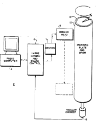
Figure 1 depicts, in block diagram form, an imaging
station 2, which may ~ s~ L an ;ntl~r-~n~nt plat~ k;n~
apparatus or an integral assembly within a printing pre6s. In
the latter case, the station 2 may be used both to image
printing plates "on press, " and to subsequently print the
desired material. It should be understood that multiple
stations 2 may be employed to meet the requirements of a
particular application. For example, a four-color spark
discharge imaging and printing system may employ a total of
four stations like the one depicted in Figure 1.
The statiQn ~ is controll2d ~ prFss computer 4. Th~
computer 4 is interfaced to an image length and swath control
unit 6. The unit 6 is also interfaced, via drivers 7, to a
writing head 8. The head 8 communicates with a printing plate
12 which is mounted on rotatable cylinder 10; the head 8
traverses the plate 12 axially (that is, from one side to the
other) . The cylinder 10 ; nrl~ c a cut-out portion or void 14
which allows access for securing or removing the printing plate
12. An angular encoder 16 is coupled to one end of the
cylinder 10 and to the control unit 6.
For purposes of clarity, other electrical and mechanical
rn"~r~n-~nts of the station 2 (e.g., a T -h~n;F~ for rotating the
cylinder 10, a --~h~n;~- for transporting the head 8 axially
across the surface of the plate 12, etc. ) are omitted.
Examples of such components are desc~ib2d in detail in related
U.S. Patent No. 4,911,075, which is assigned to the assignee of
the present invention, and which is hereby incorporated by
reference .
The general operation of ~the station 2 will now be
WO 92/lZ59Z PCrlUS92/00216
-7 -
2~
briefly described. Initially, image information in digital
form i6 supplied to the computer 4 by way of a magnetic tape,
disk, optical scanner, or other means of data input or
transfer. Such information typically ;nC~ Q5 a data
representation of the image which is to be formed on the
printing plate 12, as well as related control information.
Alternatively, the computer 4 may be used to generate the
information npcQc-cAry to image the printing plate 12.
In order to start the process of imaging the printing
plate 12, an operator (not shown) causes the computer 4 to
begin sending the nQrQcc Iry image data and control inf ormation
to the control unit 6. The operator may accomplish this, for
example, by using a keyboard, "mouse" or other input device to
control the press computer 4. Contemporaneously, the cylinder
10 begins to rotate, and continues to do so with a
substantially constant angular velocity. The functions of the
control unit 6 are explained in dctail ~elow. However, for
purposes of understanding the overall operation of the station
2, it is suf f icient to say that the control unit 6 regulates
the timing with which imaging data is supplied to the drivers 7
and, ultimately, the writing head 8.
As the writing head 8 receives imaging data from the
drivers 7, one or more imaging devices (not shown) d;~pocQd in
the head 8 will either discharge or not discharge, ~QrQnrl;n~
upon the binary 6tate of the data. When an imaging device
discharges, it forms an image "spot" on the printing surface of
the plate 12 (e.g., by ablation or surface transformation
following spark discharge, exposure of a sensitized plate
surface to radiation, deposition of a coating, etc. ) . An image
6pot is actually an area of the printing surface whose
characteristics are altered by the discharge.
On each revolution of the cylinder 10, the void 14
passes adjacent to the writing head 8, at which time the
imaging devices are idle and no imaging occurs. At that time,
the head 8 may be advanced in the axial direction in
WO 92~12592 PCr/US92/00216
r
2~99-~61 `
preparation for further imaging dùring the next revolution of
the cylinder 10. As these steps are repeated, the writing head
8 eventually traverses (scans) the full length of the printing
plate 12 in the axial direction (as shown in phantom) and a
complete image is formed on the printing surface of the plate
12 .
Figure 2A is a perspective view of a preferred
PmhQ~ nt of the writing head 8, which is constructed for non-
contact spark-discharge imaging. The head 8 inrlllAec an open-
ended gu~rd 18 which is curved so that it may reside in clo~e
proximity to the curved printing surface of the printing plate
12. Disposed within the guard 18 are sixteen individual styli
electrodes 20. The head 8 also includes a U-shaped support 22
which holds the guard 18 and the electrodes 20. The support 22
is attached to a printed circuit board (PCB) 24. Sixteen
tPrminAl~: 26 are attached to the rear edge of PCB 24 and each
of the electrodes 2Q is electrically c^nnectPd by a lesd 28 to
one of the tPrminAl~ 26. The tPrmin;ll~ 26 provide suitable
electrical connections for connecting the head 8 to other
ts of the station 2.
As may be seen more clearly in Figure 2B, the electrodes
20 are arranged along a "diagonal" within the guard 18. (The
slope of the "diagonal" in Figure 2B has been exaggerated for
purposes of more clearly illustrating the pl A~ ~ of the
electrodes). The electrodes 20 are spaced sufficiently far
apart to avoid electrical interference and/or grounding between
adjacent electrodes. Because spacing in the axial direction is
dictated by the desired resolution level (the spacing being
equal to the reciprocal of the dot resolution), the electrodes
are separated in the circumferential direction by that distance
required to produce the nP~rP~ry absolutP inter-electrodQ
distance. Using a 16-electrode writing head, our preferred
spacing is 0.001 inch (1 mil) in the axial direction, and 0.050
inch (50 mils) in the ci~.:u~eL~l.Lial direction.
Assume, for example, the electrodes 20 are to be used to
WO 92/l2592 P~USg2/002l6
_9_
2~99~
form image spots which are located on 1 mil centers in both the
axial and circumferential directions. Because the electrodes
20 are spaced 50 mils apart in the circumferential direction,
the firing of the electrodes 20 must be carefully controlled in
order to discharge sparks at the appropriate time6 to form
image spots in the correct locations on the printing surface.
In order to achieve spark discharges at the appropriate times,
the angular position information produced by the angular
encoder 16 must be properly "synchronized" with the physical
positions of the electrodes 20 in relation the prir.ting
surface. However, regardless of how one attempts to arrange
the electrodes 20 and calibrate the encoder 16, it is neither
economical nor practical to achieve a perfect dimensional
"match" between those _ -ntS. Accordingly, the present
invention provides a method and apparatus for correcting such
errors and controlling the size of the image in the
circumferential direction.
Referring now to both Figure 1 and Figure 3, the control
unit 6 includes a skew memory 30 which receives as an input
data from the press computer 4. Each of a plurality of swath
memories 32 also receives data from the computer ~ as an input.
The skew memory 3 0 provides data as an output to a control
logic unit 36, and also receives control information from logic
unit 36. Sensor logic unit 34 receives as an input angular
position data from the angular encoder 16, and provides as an
output Pnh~nl~Pd-resolution position data to the unit 36.
Each of a plurality of output memories 38 receives as an
input data from an associated one of the swath memories 32. In
addition, each output memory 38 receives as an input control
information from the unit 36. Each of the output memories 38
provides as an output imaging d~taJ ~hich i5 transmitted to an
associated one of the drivers 7. In addition, unit 36 provides
control information to the drivers 7, a void position status
signal to the computer 4, and initialization information to the
sensor logic unit 3 4 .
WO 92/12~92 PCr/US92/00216
--
~ 20995~61
Figure 4 shows a pref erred ~ - - i r - nt of the skew memory
30. In this P~ho~ L, the memory 30 include6 an area of
random access memory (RAM) 31 and an address generator
(counter) 33. RAM 31 provides an array capalble of 6toring N x
16 bits of data. RAM 31 is connected to receive sixteen data
bits in parallel from the press computer 4, which bits are
referred to herein as a "word" of "correction data. " RAM 31 is
also connected to receive from address generator 33 sixteen
addres6 bits in parallel, as well as an OUTPUT ENABLE signal
and a WRITE signal from the control logic unit 36. The address
generator 33 is connected to receive an lNC~ signal and a
RESET signal from the unit 36. The functions of the various
6ignals applied to the skew memory 30 are P~lA; nP~l in detail
below .
The RESET signal operates to set the address generator
to a predetPrm;ned starting address, which is simply the
address that is designa~ed to contain correction data
c~rL~ J~ ;ng to the first possible discharge location (in a
circumferential sense) in a given swath of the imaging area.
The term "swath" is used herein to refer to the maximum image
area which the writing head 8 can cover during one revolution
of the cylinder. The INCREMENT signal causes the address
generator 33 to advance the address applied to RAN 31 by one.
The WRITE signal permits data received from the press computer
4 to be stored at the address supplied by the address generator
33. The OlrrPUT ENABLE signal permits the transmission of a
correction data word, stored at the address supplied by the
address generator 33, to the control logic unit 36.
The size of the skew memory 30 (i.e., the value of N)
depends upon the desired image correction resolution and the
size (in the circumferential direction) of the i~aage which is
to be created. For example, if a correction resolution of
0.0001 inch (0.1 mil) is desired and the circumferential length
of the image is 16 inches, then the skew memory 30 would need a
capacity of N = 16/0.0001 = 160R. ~ccllm;n~ that the desired
WO 92/12592 PCr/US92~00216
~*
_ _
--11--
ios~si
~ g~g resolution is 1 mil in the circumferential direction,
the correction resolution would be ten times greater than the
imaging resolution. That is, in thi6 example, the skew memory
30 contains ten words of correction data for each 1 mil of
distance in the circumferential direction. If a writing head
having sixteen ele.:LLode~ like the one shown in Figure 2A is
used, and the same assumptions are made with respect to the
desired resolution, then the skew memory 30 requires a minimum
capacity of 160K x 16 bits to simultaneously store all of the
correction data for one revolution of the plate 12.
In a preferred ~-' ';r-nt, the skew memory 30 is
implemented using a RAM organized as an array of 262K x 16
bits. The additional capacity (approximately 102K) over and
above what is strictly needed for the skew memory 30 allows the
RAM to be used for other, unrelated purposes when it is not
needed to serve as the skew memory. The actual size or
configuration of the skew me~ory 30 may be vzried ~l~rpn~sinq
upon the desired correction resolution, the number of imaging
devices, and other factors such as whether the data stored in
the skew memory 3 0 is - - ~ssed or encoded, etc .
With reference again to Figure 3, the number of swath
memories 32 and associated output memories 38 required depends
upon the number of imaging devices in the writing head 8; in
the ~ho~l;~ t shown, there is one swath memory 32 and one
output memory 38 for each imaging device in the writing head.
Thus, using the sixteen-device writing head as shown in Figure
2A as an example, a total of sixteen swath memories 32 and
sixteen output memories 38 are required.
Each swath memory 32 is preferably implemented using a
RAM and an associated address generator, similar to the
arrangement shown in Figure 4. However, each sw~th memory 32
is connected to receive imaging data from the press computer 4,
as opposed to correction data. The imaging data is a
representation of the image which is to be formed on the
printing surface of the printing plate 12. In addition, each
WO 92/12592 PCr/US92/00216
2- 2~9956I
swath memory 32 and its associated address generator are
connected to receive OUTPUT ENA~3LE, WRITE, INCREMENT and RESET
signals from the control logic unit 36, which signals are
functionally similar to, but separate from, the signals applied
to the skew memory 3 0 .
The size of each swath memory 32 depends upon the
maximum number of image-spot locations in the circumferential
direction per revolution of the printing plate 12 ( imaging
resolution). For example, if image spots on 0.001 inch (1 mil)
centers are desired and the circumfer~ntial length of the image
is 16 inches, the maximum number of locations for one
revolution of the plate 12 is 16/0.001 - 16,000 locations for
each imaging device. Therefore, in this example, each swath
memory 32 requires a capacity of 16K bits in order to
simultaneously store one bit of imaging data for each possible
image-spot location along one revolution of the plate 12.
It sho~ld be noted, however, that i~ not r~G~cs~ry to
use sixteen separate memories to implement the swath memories
32. Preferably, a single RAM organized as an array of 16K x 16
bits is used to physically implement sixteen swath memories 32.
Again, the size or configuration of the swath memories 32 may
be varied ~lPrPn~; ng upon the requirements of a particular
application, such as the required imaging speed, the
circumferential length of the image, whether the imaging data
is encoded or compressed, the desired imaging resolution and
the like.
In contrast to the swath memories 32, each of the output
memories 38 preferably comprises a conventional first-in-first-
out (FIFO) memory having six one-bit storage locations. In
order to provide in-lPrPntlPnt control of the discharge from each
individual imaging device, the advantages of which are
explained below, it is preferred that the output memories 38 be
implemented as separately controllable units.
Figure 5 depicts a preferred embodiment for the control
logic unit 36. The unit 36 includes four counters 35 which are
WO 92~t2592 - PC~/USg2/00216
-
--13-- .
2~9~5~1
int~Lc....~e..Led with an algorithmlc state machine (ASM) 37.
Counter 35a is connected to receive position pulses from the
sensor logic unit 34. Each of the position pulses from unit 34
represents a predetorminPd unit of distance in the
circumferential direction around the printing surface of the
printing plate 12. Preferably, each position pulse produced by
the unit 34 ~e~Laser-Ls 0.0001 inch (O.1 mil) of distance in the
circumferential direction.
ASM 37 may be implemented, for example, by storing data
in a p~OyL hl ~ read-only memory (PROM) which represents a
control algorithm. That is, for each possible combination of
address signals that is applied to the PROM, a predetorm;no-l
combination of output (data) signals are produced by the PROM.
It should be understood that control logic unit 3 6 may be
implemented in any of a variety of ways ~oron~; ng upon the
requirements of a particular application. For example, a
mic ~ Locessor or mi~:L~col~Lruller, al~ng with an area of non-
volatile memory f or storing instructions, may be programmed in
a conventional manner to perform the functions of ASM 37.
ASM 37 is connected to receive both position pulses and
home pulses from the sensor logic unit 34. A home pulse is
preferably a single pulse which occurs once per revolution of
the cylinder 10, which serves as a marker to indicate when a
revolution is completed.
Counters 35 produce output signals which indicate when
the following conditions occurs: (1) the beginning of the
imaging area on the printing surface of the plate 12 is
approaching the writing head 8; ( 2 ) the end of the imaging area
i6 approaching; (3) the beginning of the void 14 is
approaching; or (4) the end of the void 14 is approaching. It
should be no~ed that the term "imaging area, " as used herein,
means the portion of the total printing surface area in which
an image may be formed, and excludes the "margins" or borders
which are left blank. ~hese conditions are detected in a
straightforward manner by first initializing each of the
. _ _ _ _ _ _ _
WO 92/12592 PCr/US92/00216
209~561
', .
counter6 35 to a predetermined value, and then in~L Ling the
appropriate counter in response to the position data received
from the sensor logic unit 34.
For example, assume that just a6 a revolution of the
cylinder lO is completed, the counters 35 are ir,it~lAli~ to
pr~ rmi ned starting values . The starting values for the
counters are initially calculated by knowing the
circumferential di6tance represented by each position pulse,
the circumference of the plate 12 and the angular extents of
the void l~ and imaging area. The starting values are
preferably chosen such that each counter 35 will reach its
maximum value contemporaneously with the oc- uLL~1,ce of the
condition of interest (e.g., the he~innin~ of the void).
Initialization of the counters 35 occurs when a RESET signal is
applied to the counters by the ASM 37, at which time each
counter is set to a value ~ res~l.Led by the signals present at
the inputs of the counter .
As the cylinder lO begins a revolution, position pulses
are received by the counter 35a, which is incL~ Led by each
such pulse. When the counter 35a reaches its maximum, an
~sFC, I NN I N~i OF IMAGING AREA signal is transmitted to the ASM 37,
which indicates that the beginning of the imaging area is
almost adjacent to the writing head 8. Contemporaneously, the
position pulses are applied to counter 35b, which begins to
increment in response thereto. Thus, in succession, each of
counters 35b, 35c and 35d reaches its maximum value and
transmits its respective signal to the ASM 37. The entire
process is repeated for each revolution of the cylinder lO.
The control information supplied by ASM 37 to the output
memories 38 consists of three signals: STEP DATA IN, STEP DATA
OUT and RESET. The STEP DATA IN signal operate~ to s~rially
load (from the output of the associated swath memory 32) a
single data bit into the output memory 38, while the STEP DATA
O'JT signal is used to serially transmit a single data bit from
the memory 38 to an associated driver 7. The RESET signal
WO 92/12592 PCr/US92/00216
~ ,=,,
--15--
2099~61
clears the output memories 38.
The control infor~ation supplied by ASM 37 to the
drivers 7 consists of pulses which are used to initiate firing
of the imaging devices, which pulses are described below in
connection with Figure 9A.
The detailed operation of the control logic unit 36 will
now be described, with reference to Figures 5, 6 and 8A.
operation starts at step 42 upon power up of the station 2.
The unit 6 initializes at step 44, during which the ASM 37
issues a RESET signal to the skew memory 30, which operates to
set the address generator 33 to the prP~lPtPrminpd starting
address previously de6cribed. Similarly, the ASM 37 issues a
RESET signal to the swath memorie6 32, which sets the address
generator(s) associated with such memories to predetprminp~l
starting addresses. The starting address for a swath memory 32
is simply the address which is designated to contain imaging
data c-~r~ ~n. ~ i n~ to the ~irst imag~e spot (whether blahk Gr
not) of a given swath of the image. A RESET signal is also
issued to the output memories 38, which clears them. The unit
36 also provides initialization information to the unit 34
(which is described below in connection with Figure 10 ) and
sets the four counters within the unit 36 which are used to
detPrminP the boundaries of the imaging area and the void 14.
In addition, the skew memory 30 is loaded by the
computer 4, in co~eLation with the unit 36, with prP~PtPrminpcl
correction data which will be used to prevent the slanted swath
condition and to control the size of the image in the
circumferential direction. The loading of the skew memory 30
entails the assertion of a WRITE signal from the unit 36,
followed by transmission of a word of correction data from the
computer 4, which word is stored in the S~fl~f m~hiory 3 0 at the
address specified by the address generator 33. An lNC.~I~l
signal is then issued from the unit 36, which increments the
address generator 33. This process continues until all of the
correction data is stored in the skew memory 3 0 . In general,
_ _ _ _ _ . . . . . .. . .. _
WO 92/12592 PCr/US92/00216
2099561
--16--
_
the 6kew memory 30 ifi loaded only once during initlAli7at;nn
and the correction data stored therein is used for all
subse~auent imaging.
A method f or deriving the correction data u6ed in the
skew memory 30 will now be described. In this example, assume
that a four-color imaging and printing system having four
imaging stations 2 is u6ed. Further a6sume, a6 before, that an
imaging re601ution of 1. 0 mil and a correction re601ution of
0.1 mil are desired.
Fir6t, each of the f our imaging 6tations 2 i6 u6ed to
image and print a "6tandard" te6t pattern. For these test
pattern runs, the skew memory 30 is loaded with "nominal" or
neutral correction data, which essentially allows the te6t
pattern image data to pa66 through to the driver6 7 without
adju6tment in the circumferential direction. A6 6hown in
Figure 7A, "nominal" correction data for the 6kew memory 30 may
Con&iEt of storing all binary one6 at the f~rst adæ~e66 Gf the
skew memory 30 (CUL1~ 1;n~ the first pos6ible di6charge
location on a given revolution of the cylinder 10), followed by
all ~inary zero6 in the next nine successive addre66es, and
repeating this pattern through the entire skew memory 3 0 . The
effect of 6uch "nominal" correction data is simply to allow one
bit of imaging data to be advanced from the output memories 38
to the drivers 7 every 1. 0 mil of distance in the
circumferential direction, which represents the distance
between nominal image-6pot location6.
Once the te6t image6 are complete, physical mea~uL~ Ls
can be made to determine by how much the image sizes differ.
From these mea6urement6, one may calculate how much to shrink
or increa6e the image produced by each imaging station in order
to achieve four image6 of the same sizs. The de6ired shrinkage
or enlargement is implemented by altering the "nominal"
correction data. Assume that it i6 nec~csAry to shrink the
length of an image by 0.1 mil. This could be implemented by
modifying the correction data as shown in Figure 7B. There,
WO 92/12592 PCr/US92/00216
, .
--17-- = -
2~99~1
the correction data word stored at the tenth address of nemory
30 is changed to all binary ones, meaning that the
corrC~Rp~n~l i ng imaging data is advanced to the drivers 7 at a
slightly earlier time (i.e., 0.1 mil in circumferential
distance) as compared to the nominal correction data shown in
Figure 7A. Thus, if the r~ ;nin~ correction data is
~ h:~n~ed, the circumferential length of the image decreases
(shrinks) by 0.1 mil.
Desired amounts of enlargement or shrinkage in the
circumferential direction, within the limits of the imaging
area of the printing plate 12, may be spread uniformly, or
otherwise, across the length of the image by selectively
altering the correction data values stored in the skew memory
30 .
Referring again to Figure 6, at step 46, the swath
memories 32 are loaded with imaging data for the first swath to
be imaged on the printing ~urface of the plate 12. The swath
memories 32 are loaded in a manner similar to that de6cribed
above with respect to the skew memory 3 0, except that imaging
data is loaded instead of correction data. Using again the
assumptions of a circumferential image length of 16 inches and
image spots on 1 mil centers, a total of 16K x 16 image data
bits are loaded by the pre6s computer 4 into the swath memories
32 during step 46.
At step 48, as shown in Figure 8B, the unit 36 issues an
OUTPUT ENABLE signal to the swath memories 32 and a STEP DATA
IN signal to the output memories 38, which causes the first
data bits appearing at the outputs of the memories 32
(collectively, a sixteen-bit word of image data) to be advanced
into the first storage locations of memories 38. The unit 36
then i~sues an ~NCREMENT signal to all of the swath me~ories
32, which causes their respective address generators to
increase by one. An OUTPUT ENABLE signal is again issued to
the swath memories 32 and the steps are repeated until a total
of three bits of image data are stored in each of the output
WO 92/12592 PCr/US92/00216
2~99~61
--18--
~ _ .
memorles 38, and the address generators for the swath memories
32 are set to the addresses for the fourth bits of image data.
Once the f irst three bits of the f irst swath of image
data are advanced into the output memories 38, the station 2 is
ready to actually start imaging at 6tep 50. By this time, if
not earlier, the cylinder l0 is rotating at a generally
constant angular velocity, and angular position data generated
by the sensor logic unit 34 is tr~nsmitted to the unit 36. The
unit 36 also receives a word of correction data from the skew
memory 30 (the word stored at the address corr~p~nA;ng to the
predetPrm; nr~cl starting address) . By detecting the receipt of a
home pulse, the unit 36 may associate or ~y~ L~ ize a known
angular position of the cylinder l0 with this f irst word of
correction data . Pref erably, the f irst word of correction data
is synchronized with the f irst possible discharge location of a
given swath, thereby synchronizing subsequent correction data
words seguentially with succes~ive possible discharge
locations .
Each correction data word stored in the skew memory 3 o
indicates whether the image data for a particular imaging
device should be advanced to the drivers 7 . In a pref erred
L, the eighth bit (L.ULL~ llA;nrJ to the eighth imaging
device of a sixteen-device writing head) of the sixteen-bit
correction data words is used to indicate when the next word of
image data stored in the ~wath memories 32 should be advanced
to the output memories 38. If the eighth bit of the output
word from the skew memory 30 is a binary one, the imaging
control process continues to step 54.
Although the eighth bit of the correction data words has
been chosen for purposes of illustrating the "trigger" for
advancing data from the swath memories 32 to the o~utput
memories 3&, the ninth bit would function in a comparable
manner. The significance of the eighth bit is that it
corresponds to the eighth imaging device, which is physically
close to the exact middle of a sixteen-device swath.
WO 92/12592 _ PCrtUS92/00216
.~
--19-- ~ "
2~9~5~
,
Therefore, the eighth bit (imaging device) is a logical choice
as a "reference" whose actual discharge location is neither
advanced nor retarded from it6 nominal location. Viewed
another way, only the discharges L;~LL ~ in~ to bits other
than the eighth bit are subject to being moved forward or
backward, thus producing a skew about the eighth bit.
During step 54, the unit 36 issues a STEP DATA OUT
signal to those output memories 38 whose C~JLL ~ ; n~ bits in
the output word from the skew memory 38 are binary ones. Due
to the conditional test of step 52, it is known that at least
the eighth bit of the output word from the skew memory 38 is a
binary one. Therefore, at least that output memory 38 which
corresponds to the eighth imaging device will be issued a STEP
DATA OUT signal at this time. D~p~n~;n~ upon the binary values
for bits 1-7 and 9-16 of the output word from the skew memory
30, the output memories 38 which correspond to those bits may
be issued their STEP l;~ATA OUT signals slightly before or
slightly after that which is issued with respect to the eighth
imaging device. In this fashion, each output memory 38, and
the firing of its associated imaging device, may be
;n~r~n~ ntly controlled by the unit 36.
The potential time differences in the ;Ccll~nr~e of the
STEP DATA OUT signals to different output memories 38 represent
a "skewing" of the image data as it is presented to the driver6
7, and ultimately to the imaging devices. It is this skewing
which effectively tes for any error between the angular
encoder 16 and the imaging devices.
Also during step 54, in conjunction with the issuance of
the STEP DATA OUT signals, the unit 36 send6 a control signal
to the drivers 7 which actually initiates the discharge of the
individual imagin~ devices. The unit 36 then ~sserts an
lN~ signal to the swath memories 32, which cause6 the
next word of image data to appear at the outputs of the
memories 32. This is followed by a STEP DATA IN signal to the
output memories 38 which advances the data word into the output
WO 92/12592 PCr/US92/00216
209~561 ~
--2 l7--
,
,, , ~, ~, ~
memories 38. The skew memory 30 address is then advanced at
step 56 by the assertion of the INCREMENT signal by the unit
36 .
If, during step 52, the eighth bit of the output word
from the skew memory 3 0 is not a binary one (meaning that no
image data is to be advanced to the output memories 38 at that
particular time), the imaging control process bypasses step 54 ,
and moves to step 56 in which the unit 36 issues an INCREMENT
signal to in~ the address of the skew memory 30. In
response, the next sequential word i5 output by the skew memory
30 and is Dy~inP~7 by the unit 36. If any of the bits of the
output word is a binary one, the unit 36 will issue a STEP DATA
OUT signal to the CU1L ~ 7;ng output memory 38 and also send
the Cl~1JLU~L iate control signal to the drivers 7 .
7~e~ ;~11 ;n~ the example from above, in which the desired
correction resolution was O. l mil and the imaging re601ution
was 1. O mil, one will remember that the skew me.lory 30 contains
ten words of correction data c.,-L-~ n~7;n~ to each l.O mil of
circumferential distance. That explains why the address of the
skew memory 30 is advanced multiple times between advances of
the swath memories ' addresses. Therefore, by specifying which
bits of the words stored in the skew memory 30 contain a binary
one, the actual discharge locations may be moved forward or
backward (circumferentially) by a desired nuD7ber of 0 . l mil
increments to prevent the slanted swath condition and to adjust
the image size.
At step 5&, the unit 36 checks the cumulative number of
position pulses received from the unit 34 since the beginning
of the current revolution of the cylinder lO. Based on the
pulse count, the unit 36 rl~t~rm;n~c whether the cylinder lO has
rotated sufficiently far so that the writing head- 8 ha~ reached
the end of the imaging area for the current swath (e.g., is the
END OF IMAGING AREA signal present). If the end of the imaging
area has not been reached, the imaging control process returns
to step 52 and, as before, checks the eighth bit of the output
_ _ _ .,, . ,, , : , , . _ ,,, ., , , _
WO 92/12592 PCI/US92/00216
--2 l--
2~9~
word from the skew memory 30 to determine whether to advance
additional image data to the drivers 7.
If, during step 58, it is det~rm;n~d that the current
swath is complete, meaning that the void 14 is approaching the
writing head 8, the process continues to step 60 during which
the unit 36 asserts the VOID POSITION STATUS signal. While
that signal is asserted, the press computer 4 is permitted to
transmit new image data into the swath memories 32. As the
void 14 complete6 its pass by the head 8 (the END OF VOID
signal occurs), the unit 36 stops asserting the VOID POSITION
STATUS signal and the computer 4 is prevented from transmitting
further imaging data to the swath memories 32.
During step 62, the unit 36 ~Pterm; n~: whether the image
i5 complete. That determination is made by r~h~ i n~ the swath
memories 32 to determine whether new image data was actually
loaded by the press computer 4. If not, meaning that no more
image data remains, the Lmage i~ co~21~te and the proce.,s ends
at step 64. If 50, meaning that there is at least one more
swath of imaging to perform, the process returns to step 48 and
proceed6 as before. Steps 60 and 62 are preferably executed
during the period of each revolution when the void 14 is
adjacent to the writing head 8, thus allowing the 6tation 2 to
prepare to image the next swath during the time when the
writing head 8 is normally idle.
Figure 9A is a circuit diagram of a suitable one of the
drivers 7 shown in Figure l, conf igured to operate a spark-
discharge electrode. A monostable multivibrator 66 is
connected to receive, as inputs, pulses from the control logic
unit 36. An output of the multivibrator 66 is connected to one
input of an AND gate 68. A second input of the AND gate 68 is
connected to receive imaging data f~om one of the output
memories 38. An output of the AND gate 68 is connected to the
input of a high speed, high current MOSFET driver 70, whose
output is connected to the gate of a MOSFET 72. The source of
the MOSFET 72 is connected to ground potential.
_ _ _ . . . _ ~ .
WO 92/12592 PCr/US92/00216
2~9g56~ --
--22--
__ _
,;,
A primary winding of a transformer 76 i6 connected
between the drain of the MOSFET 72 and a voltage supply(500
VDC). A diode 74 is connected in parallel with the primary
winding, with the anode of the diode connected to the drain of
the MOSFET 72. One end of a ~Pcnn~3~ry winding of the
transformer 76 is connected to ground potential. A resistance
80 is connected between the ~econd end of the ~econ~ry winding
and the anode of a diode 78, whose cathode is connected to
ground. A resistance 82 is connected in series between
resistance 80 and an electrode 20.
The operation of the driver circuit 7 may be understood
best with reference to both Figures 9A and 9B. As imaging data
is applied from the output memory to the AND gate 68 and a
pulse is output from the multivibrator 66 in response to a
control signal from unit 36, AND gate 68 generates a fire
pulse, which is amplified by driver 70 and applied to the gate
of MOSFET 72. It sho~d be apparent that only i. aging data
having a binary value of one associated with a prPdetPrm; n~d
voltage level will generate a fire pulse, since the
complementary binary value (zero) simply means that the space
is to be left blank.
The duration of the fire pulse is on the order of l00
n~nn5Prnn~ and its magnitude is approximately 5V. In response
to the fire pulse, the drain voltage of the MOSFET 72 decreases
rapidly from the supply voltage to zero. In turn, there is a
rapid decrease of the electrode voltage (referenced to the
cylinder l0, which is connected to ground potential) to
approximately -4,500 volts, which results in discharge of a
spark from the electrode 20 to the printing surface of the
printing plate 12, thereby forming an image spot.
In order to achie~e ~atisf~ctory imaging speeds, the
driver circuit 7 must and does achieve a rise time on the order
of l09 volts/second in producing the electrode voltage. In
addition, protection should be provided such that excessive
currents and incorrect electrode voltage polarity are avoided.
WO 92/t2592 PCr/US92/00216
.
--23--
~D93~1
Resi6tance 82 serves to limit the current delivered to the
electrode 20, while resistance 80 in combination with diode 78
provide a clamp which prevents the polarity of the electrode
voltage from ~ - ; n~ positive with respect to ground.
Figure 10 is a circuit diagram of the sensor logic unit
34 shown in Figure 3. The major ~ -- L.s of the unit 34 are
a phase locked loop (PLL) 84, a first lJL~yL hle divider 86
and a second ~Lo~L~able divider 88. PLL 84 consists of a
phase comparator 90 having a first input which is connected to
t~.e angular encoder 16 tFigure l). An output of the comparator
go is connected to the input of a low pass filter 92. The
output of the filter 92 is connected to the input of a voltage
controlled oscillator tVCO) 94. The output of the VCO 94 is
fed back, via the divider 96, to a second input to the
comparator 90. Lastly, the output of the VCO 94 is connected
to the input of the divider 86.
The dividers ~6 and 96 are pr~ d by th2 unit 36 as
part of the initialization step 44 tFigure 6). That is, each
divider is loaded with a integer value tP or N) which functions
as its divisor. The selection of appropriate integer values
depends on ~everal factors, inr~ in~ the desired position
resolution, the resolution of the angular encoder 16 and the
diameter of the plate cylinder. As an example, assume that the
divisor P=1, the encoder generates 2 . 5 x 10³ pulses per
revolution, the desired position resolution is 0.1 mil in the
circumferential direction, and the plate cylinder has a 8 inch
diameter. Thus, to calculate the value of N, one would first
calculate that there are tpi) t8 inches)/O.oO1 inch = 2.513 x
105 increments (each 0.1 mil in length) around the
circumference of the cylinder. Therefore, N = 2 . 513 x 105/2 . 5
x 103 = 100 or 101 rounded to the nearest integ2r. HoWeve}, ~f
N=lOO, each in~ L~ Lal integer change in N represents a change
of approximately 196 in distance per pulse, which may introduce
unacceptable error.
A solution to this problem is to simply multiply both P
WO 92/l2592 PCr/US92/00216
2~995~1 --
--2~--
. . .
and N by the same value. If, in the last example, P=10 and
N=1000, then an in~;L~ ~al integer change in the value of N
rc~.~6~ ..Ls a change of approximately 0.1% in di6tance per
pulse. Moreover, even though the angular encoder produces only
2, 500 pulses per revolution, the output of divider 86 provides
250, 000 pulses per revolution or one pulse for each 0.1 mil of
distance in the circumf erential direction .
It should be apparent that other desired resolutions may
be obtained by altering the values of the divisors.
In effect, the sensor logic unit 34 operates to enhance
a relatively low resolution angular position signal produced by
the angular encoder to yield a position signal having a
substantially ~nhAnced resolution. As a result, a relatively
inexpensive, off-the-shelf angular encoder may be employed, yet
sufficient angular position resolution is obtained.
We will now discuss minimiP~tion of periodic "streaking"
artifacts associated with multiple-device writing heads. Refer
to Figure llA, which shows a series of complementary image
rL~,_ - Ls 120~, 120b, 120_ and 120_ printed by black, magenta,
cyan and yellow printing plates, respectively. Each plate i5
imaged by an i n/l~r~n~-nt image or writing head depicted
generically at 122 and shown schematically at 122a, 122_, 122c
and 122d. Each head itself inrl~ 16 imaging devices that
traverse the plate in the indicated direction of relative
motion. At the conclusion of each circumferential scan (and
before the beginning of the next scan), the head i5 shifted, or
stepped, to the left by an amount sufficient to place the first
imaging device of the array adjacent the next scan line.
The four vertical lines in each fragment represent
streaked printing artifacts caused by any of the flaws
described above. Because the streaks recur at intervals eS~ual
to the width of the writing heads, one can infer that a single
flaw is associated with each head. Specifically, the
illustrated positions of the streaks suggest that, in each
case, the lead imaging device is responsible.
_ _ _ _ _ _ _ _ _ _
WO 92JI2592 PCrJlJS92/00216
--25--
2~99~1
During printing, the four image fragments 120~, 120k, 120c
and 120_ are sequentially impre6sed onto the same physical
location of the recording medium; in other words, they are
printed in register. The final composite image, representing
these fragments overlaid one on another, is indicated by
reference numeral 124. Because they are printed in register,
the four vertical artifacts reinforce one another, as shown by
the heavy vertical lines.
Our solution to thi6 problem is shown in Figure llB.
Essentially, it involves staggering the initial imaging
positions of the writing heads, so that artifacts caused by
similarly situated elements within the heads do not appear at
the same positions on the plates, and also appear less visually
prominent due the their proximity to one another. Thus, in
Figure llB, writing head 122a (CULL~ 1;n~ to black) begins
imaging at the same initial position as was the case in Figure
llA. ~lowever, writing head l22k (CUL1. ~L,....~1;n~ to magenta) is
positioned only partially over the imaging area such that
during the initial imaging pass, only the last four (of
sixteen) imaging devices actually cover and produce discharges
on the image area. After the first pass, writing head 122_ is
advanced by the usual stepping amount, and all 16 imaging
devices are active (as shown by the S~1~CC~ ; ng set of circles);
however, since the first pass was staggered, the position of
each successive magenta vertical artifact is advanced by one-
fourth the width of the writing heads. Similarly, only the
last eight imaging devices of writing head 122c (~LL~byonding
to cyan) produce discharges during the f irst imaging pass,
thereby advancing the position of each successive cyan artifact
by one-half the width of the writing heads, and only the last
twelve imaging d~vices of writing head 122d (CorrP~pnn~?;ng to
yellow) produce discharges during the first imaging pass,
thereby advancing the position of each successive yellow
artifact by three-fourths the width of the writing heads.
During successive scans, all of the imaging devices are
WO 92/12592 PCrtUS92/00216
2~99~61
, ` d --
-26-
selectively activated as di ~c~ d hereinabove to produce image
swaths. (The stagger amounts associated with each color are
given for illustrative purposes only; there is no advantage to
associating a particular stagger amount with a specif ic color. )
The final composite image is indicated by reference
numeral 126, and shows how the vertical artifacts are closely
and evenly spaced from one another. The same effect can be
obtained, for example, by selecting a different imaging device
in each array as the first device, thereby reducing the number
of i~aging devices that write during the f irst pass, and
producing truncated swaths of differing widths. After this
first pass, each head is stepped by a cu~ yol~dingly smaller
amount, so that at the second pass, the heads are positioned to
produce full swaths at identical plate locations.
In one ~ nt, the imaging devices of each writing
head are non-contact electrodes axially spaced 0. 001 inch apart
(as shown in Figure 2~); the total width of e3ch head, then, i8
0. 016 inch. Without staggering, the artifacts shown in Figure
llA will occur each 0.016 inch, CULL~ r~ ;n~ to a frequency of
62.5 artifacts per inch. This frequency is 6mall enough to be
perceived by the human eye. Using the technique described
above, the artifacts occur each 0. 004 inch, or at a frequency
of 250 artifacts per inch; under ordinary lighting and viewing
conditions, the human eye cannot resolve such closely spaced
f eatures .
By evenly staggering the writing heads, the distance
between artif acts can be reduced to a length equal to the width
of each writing head divided by the total number of heads. It
should also be noted that this technique can be applied to
imaging systems having any number of i ndPrPn~nt heads and
~ma~ing devices within each head.
In the above example, we stipulated that the streak
artifacts were caused by malfunction of the lead imaging device
in each head. In fact, we have observed just such a phPr~ ~n
on a variety of plate constructions using the writing head
, . . _ ~
WO 92/12S92 _ PC~US92/00216
--2 7--
shown in Figures 2A and 2B . The f irst electrode to image the
printing surface after stepping tend6 to ablate plate-surface
material less strongly than the 8-~ cee~; n~ electrodes in the
array; this is found to be 80 regardless of which electrode is
selected to image f irst . We are uncertain as to the precise
cause of this behavior, although we believe that it may be due
to debris from the previous imaging pass acting as an
insulator, or to field effects due to the shape and electrical
capacity of the plate metal at edges created by the previous
imaging pass, or to a combination of both of the~ie effects.
The staggering technique described above can be used to
minimize the visual impact of this rhPr ; alternatively,
the drive circuitry can be modif ied to apply greater voltage
and/or current to the lead electrode in order to - -ate for
the deficiency in ablation.
The foregoing description has been limited to a specific
embodiment of this invention. It will be al?p~ L~ however~
that variations and modifications may be made to the invention,
with the at~A; t of some or all of the advantages of the
invention. Therefore, it is the object of the ArpPn~d claims
to cover all such variations and modifications as come within
the true spirit and scope of the invention.
What is claimed as new and desired to be secured by
Letters Patent of the United States is: