Note: Descriptions are shown in the official language in which they were submitted.
2099~4~
1 BACKGROUND OF THE INVENTION
The present invention relates to switches for
controlling currents flowing in both directions such as
alternate currents, and particularly to a solid-state
switch formed of semiconductor devices, such as gate
turn-off thyristors, connected in series in order that it
can be operated at a high voltage.
When a solid-state switch is used as, for
example, a breaker in a power system, the solid-state
switch must withstand a high voltage because the nominal
voltage of the transmission lines is, for example, 3.3 kV
through 500 kV, and because several times the system
voltage is applied to the breaker after current is cut
off. However, a single semiconductor device cannot
satisfactorily withstand this high voltage, and thus
several semiconductor devices are required to be
connected in series to increase the breakdown voltage of
the switch. In addition, in the power system, an AC
current must be flowed and cut off.
When gate turn-off (GTO) thyristors are used to
make a solid-state switch, diodes for protecting the GTO
thyristors from the reverse voltage are necessary to be
connected in series with the thyristors because the
reverse breakdown voltage of the GTO thyristors is often
much lower than the forward breakdown voltage. Some
20~9~
- 2 -
1 solid-state switches formed of these gate turn-off
thyristors have been proposed for controlling alternate
currents. In one of those switches, the gate turn-off
thyristors of an arm for forward current and those of the
other arm for reverse current are connected in an
inverse-parallel (reverse-parallel) configuration. In
another one of those switches, diodes are connected in a
bridge configuration, and a gate turn-off thyristor is
connected at the center of the bridge. Moreover, these
solid-state switches as the basic circuit arrangements
are connected in series in order to withstand a high
voltage that will be applied when the solid-state
switches are turned off.
SUMMARY OF THE I NVENT I ON
Accordingly, it is an object of the invention
to provide a solid-state switch which can be formed of a
small number of gate turn-off thyristors and which does
not greatly increase the current-flowing loss, or watt
loss.
When a series circuit of gate turn-off thyris-
tors 200 and diodes 300 for reverse voltage protection
and another series circuit of gate turn-off thyristors
200 and diodes 300 are connected in an inverse-parallel
(reverse-parallel) configuration as shown in Fig. 2 to
form a high-voltage resistant solid-state switch with the
forward breakdown voltage increased, two arms are neces-
sary for controlling the forward current and reverse
2~999~4
-- 3
1 current, and thus the total number of gate turn-off
thyristors used is increased twice the number of gate
turn-off thyristors used in a series circuit which is
determined by the high voltage that is applied when the
solid-state switch is turned off and by the set voltage
across each of the gate turn-off thyristors. In the
circuit arrangement shown in Fig. 2, two gate turn-off
thyristors are connected in series to totally increase
twice the breakdown voltage of each thyristor. Thus,
this solid-state switch has four gate turn-off thyristors
and four diodes for reverse current protection. The
current in each direction flows in the four semiconductor
devices, so that the watt loss is increased the more.
The gate turn-off thyristor is several times expensive as
compared with the diode of the same size. Thus, since
the number of gate turn-off thyristors used is twice that
determined by the turn-off breakdown voltage of the
solid-state switch, the number of drive circuits for the
gate turn-off thyristors is increased so that the solid-
state switch becomes large-sized and expensive. Fig. 3
shows a bridge-type solid-state switch in which the
diodes 300 for reverse voltage protection are connected
in a bridge configuration and in which the gate turn-off
thyristor 200 is connected in the center of each bridge.
In this circuit arrangement, the number of gate turn-off
thyristors used is the same as the number of series-
connected ones that is determined by the high voltage
that is applied when the solid-state switch is turned off
2 0 ~
-- 4
1 and by the set voltage of each of the gate turn-off
thyristors, but the number of diodes used is increased.
Since the number of semiconductor devices in which a
current is flowed is increased 1.5 times that of the
reverse-parallel connection type shown in Fig. 2, the
semiconductor devices produce a large loss when currents
are normally flowed in the devices. When two diode
bridges, each of which has a gate turn-off thyristor con-
nected in the center, are connected in series to form a
solid-state switch having twice the breakdown voltage of
each of the gate turn-off thyristors as, for example,
shown in Fig. 3, two gate turn-off thyristors and eight
diodes are necessary, and a current is flowed in six
semiconductor devices in each direction, so that the watt
loss is increased the more.
According to this invention, to solve the above
problems, there is provided a solid-state switch having a
plurality of gate turn-off thyristors connected equiva-
lently in series between the switch terminals, wherein
one of the adjacent gate turn-off thyristors has its
anode connected through a diode to the cathode of the
opposite one, the diodes connected between the adjacent
gate turn-off thyristors have their anodes connected to
the cathodes of the gate turn-off thyristors and their
cathodes connected to the anodes of the gate turn-off
thyristors, the gate turn-off thyristors adjacent to the
terminals respectively have at least, the cathodes of
their anodes and cathodes, connected through diodes to
~099~4~
-- 5
1 the switch terminals, and the diodes connected between
the cathodes of the gate turn-off thyristors adjacent to
the switch terminals and the switch terminals have their
anodes connected to the cathodes of the gate turn-off
thyristors and their cathodes connected to the switch
terminals, respectively.
According to the solid-state switch of the
invention mentioned above, the current (in some case,
flowed from the anode of the diode to the cathode
thereof) is flowed from the anode of the gate thyristor
to the cathode thereof, from the anode of the diode to
the cathode thereof, from the anode of the other gate
turn-off thyristor to the cathode thereof, and from the
anode of the diode to the cathode thereof, in turn (the
opposite current is also flowed in the same way), so that
a solid-state switch has a plurality of gate turn-off
thyristors connected equivalently in series between the
terminals.
According to this invention, if two gate turn-
off thyristors are used to constitute a solid-state
switch, the solid-state switch is able to have twice the
breakdown voltage of each gate turn-off thyristor in the
off-state. In the prior art, in order to construct a
solid-state switch having the same breakdown voltage in
the off-state as above, four gate turn-off thyristors
connected in series with diodes for reverse breakdown
protection must be connected in a reverse-parallel
configuration. In the invention, only two gate turn-off
2~9S344
-- 6
l thyristors which is 1/2 the number of gate turn-off
thyristors in the prior art may be connected to achieve
the same solid-state switch. In addition, the number of
drive circuits necessary for the gate turn-off thyristors
can be reduced to 1/2 that in the prior art, thus the
solid-state switch being small-sized and produced at low
cost. If the diodes for the reverse breakdown voltage
protection are connected in a bridge configuration, and a
gate turn-off thyristor is connected at the center of
each bridge to form a solid-state switch, 8 diodes are
necessary, and hence the watt loss in the semiconductor
devices is six times that of each device. In this
invention, 6 diodes may be used to achieve the same
solid-state switch, and hence the watt loss in the
semiconductor devices is reduced to five times that of
each device.
According to the solid-state switch of the
invention, the number of gate turn-off thyristors used
can be reduced without greatly increasing the watt loss.
BRIEF DESCRIPTION OF THE DRAWINGS
Fig. 1 is a diagram of the arrangement of a
basic solid-state switch of one embodiment of the
invention.
Fig. 2 is a diagram of the arrangement of a
conventional solid-state switch.
Fig. 3 is a diagram of the arrangement of
another conventional solid-state switch.
209994~
1 Fig. 4 is a diagram of the arrangement of a
solid-state switch equivalent to the series connection of
three gate turn-off thyristors as another embodiment of
the invention.
Fig. 5 is a diagram of the arrangement of a
solid-state switch equivalent to the series connection of
n gate turn-off thyristors as still another embodiment of
the invention.
Fig. 6 is a table of device number and loss for
a solid-state switch of an embodiment of the invention
and for conventional solid-state switches.
Fig. 7 is a diagram of the arrangement of a
solid-state switch having a series circuit of semi-
conductor devices in each branch as still another
embodiment of the invention.
Fig. 8 is a diagram of the arrangement of a
solid-state switch having a parallel circuit of semi-
conductor devices in each branch as still another
embodiment of the invention.
Fig. 9 is a diagram of the arrangement of a
solid-state switch having a series circuit of basic
solid-state switches as still another embodiment of the
invention.
Fig. 10 is a diagram of the arrangement of a
solid-state switch having a parallel circuit of basic
solid-state switches as still another embodiment of the
invention.
Fig. 11 is a diagram of the arrangement of a
- 239g~
1 solid-state switch having a parallel circuit of basic
solid-state switches connected in series as still another
embodiment of the invention.
Fig. 12 is a diagram of the arrangement of a
solid-state switch having impedance elements connected to
basic solid-state switches as still another embodiment of
the invention.
Fig. 13 is a diagram of the arrangement of a
solid-state switch having impedance elements each
connected in parallel to each of the semiconductor
devices of basic solid-state switches as still another
embodiment of the invention.
Fig. 14 is a diagram of the arrangement of a
solid-state switch having impedance elements connected
crosswise in each section of a basic solid-state switch
as still another embodiment.
Fig. 15 is a diagram showing that an impedance
element can be connected in the basic solid-state switch.
Fig. 16 is a diagram of the arrangement of a
modification of the basic solid-state switch, showing
that the basic solid-state switch is formed of gate
turn-off thyristors and thyristors.
Fig. 17 is a diagram of the arrangement of
another modification of the basic solid-state switch,
showing that the basic solid-state switch is formed of
thyristors and diodes.
20~9~4
g
1 DESCRIPTION OF THE PREFERRED EMBODIMENTS
One embodiment of the invention will be de-
scribed with reference to Fig. 1.
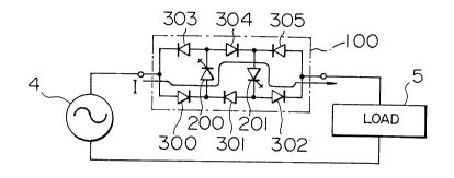
Fig. 1 is a diagram of the arrangement of a
basic AC solid-state switch 100 for AC as one embodiment
of the invention. In this embodiment, two gate turn-off
thyristors and diodes are connected in forward and
reverse directions as illustrated in Fig. 1. In other
words, the cathodes of first and second diodes 300, 301
are connected to the anode of a first gate turn-off
thyristor 200, and the anodes of third and fourth diodes
303, 304 are connected to the cathode of the first gate
turn-off thyristor 200. In addition, the anode of the
second diode 301 and the anode of a fifth diode 302 are
connected to the cathode of the second gate turn-off
thyristor 201, and the cathode of the fourth diode 304
and the cathode of a sixth diode 305 are connected to the
anode of the second gate turn-off thyristor 201. The
anode of the first diode 300 is connected to the cathode
of the third diode 303, and a terminal of the switch is
led out from the junction therebetween. The cathode of
the fifth diode 302 is connected to the anode of the
sixth diode 305, and the other terminal of the switch is
led out from the junction therebetween. Moreover,
necessary protection circuits such as snubber circuits
not shown are connected to the respective semiconductor
devices of gate turn-off thyristors and diodes.
The operation of the solid-state switch 100
2~39994~
-- 10 --
l connected between a power source 4 and a load 5 will be
described with reference to Fig. 1. We now consider that
the gate turn-off thyristors 200 and 201 are turned on so
that the solid-state switch 100 is in the on-state. A
current I is flowed through a circuit of the diode 300,
the gate turn-off thyristor 200, the diode 304, the gate
turn-off thyristor 201 and the diode 302 and through a
circuit of the diode 305, the gate turn-off thyristor
201, the diode 301, the gate turn-off thyristor 200 and
the diode 303, alternately. When the gate turn-off
thyristors 200, 201 are turned off, the current is cut
off since a series circuit of the diodes 300, 301 and 302
or a series circuit of the diodes 303, 304 and 305
includes ones of opposite polarities. When the terminal
at which the anode of the diode 300 and the cathode of
the diode 303 are connected together is at a higher
potential than is the other terminal of the solid-state
switch 100, the diode 303 functions as a reverse break-
down voltage protective diode for the gate turn-off
thyristor 200, and the diode 301 functions as a reverse
breakdown voltage protective diode for the gate turn-off
thyristor 201. When the terminal at which the cathode of
the diode 302 and the anode of the diode 305 are con-
nected together is at a higher potential than is the
other terminal of the solid-state switch 100, the diode
302 functions as a reverse breakdown voltage protective
diode for the gate turn-off thyristor 201, and the diode
304 functions as a reverse breakdown voltage protective
- - 11 20~9~
l diode for the gate turn-off thyristor 200.
It is assumed that in Fig. 1 the set voltages
across the gate turn-off thyristors 200, 201 in the off-
state are represented by e (V). Since the gate turn-off
thyristors 200 and 201 in Fig. 1 are equivalently con-
nected in series, the breakdown voltage of the solid-
state switch can be set to 2e (V). At this time, the set
voltages across the diodes 300, 302, 303 and 305 are
equally e (V), and the set voltages across the diodes 301
and 304 are equal to 2e (V). Thus, the reverse breakdown
voltage of the diodes 300, 302, 303, 305 may be selected
to be e (V) or above, and that of the diode 301, 304 may
be selected to be 2e (V) or above. Therefore, the
breakdown voltage of the solid-state switch in the off-
state can be made equal to that determined by the setvoltage and number of gate turn-off thyristors used.
Figs. 2 and 3 respectively show the circuit
arrangements of conventional solid-state switches 101,
102 having the same breakdown voltage as in Fig. 1. In
Fig. 2, a series circuit of two reverse breakdown
protective diodes 300 and two gate turn-off thyristors
200 which are connected in the forward direction is
connected in parallel with a series circuit of the same
elements which are connected in the reverse direction.
From Figs. 1 and 2, it will be seen that the number of
gate turn-off thyristors used in the solid-state switch
100 of the invention is 1/2 that of the conventional
example 1. In Fig. 3, a bridge circuit formed of four
2~g~
- 12 -
1 diodes 300 for reverse breakdown voltage protection and
one gate turn-off thyristor 200 connected at the center
is connected in series with a bridge circuit of the same
elements. From Figs. 1 and 3, it will be seen that the
number of diodes used in the solid-state switch 100 of
the invention is two ones less than the conventional
example 2, or that the watt loss in the invention is
smaller because the number of semiconductor elements in
which current is normally flowed is smaller than the
conventional example.
The diodes 300 and 305 in Fig. 1 may be omitted
because they do not function as reverse breakdown voltage
protective diodes. In this case that the diode 300 is
excluded, in order not to change the breakdown voltage
between the terminals, it is preferable to use the diode
302 of reverse voltage more than 2e [V]. Similarly, in
case that the diode 305 is omitted, it is preferable to
use the diode 305 of reverse voltage more than 2e [V].
Fig. 4 shows a solid-state switch 110 of
another embodiment of the invention, in which three gate
turn-off thyristors are connected equivalently in series.
It is assumed that the set, or breakdown voltage of each
gate turn-off thyristor 210, 211, 212 in the off-state is
represented by e (V). If the reverse breakdown voltage
of the diode 310, 313, 314, 317 is selected to be e (V)
or above, and if that of the diode 311, 312, 315, 316 is
selected to be 2e (V) or above, the breakdown voltage of
this solid-state switch in the off-state can be set to 3e
- 13 _ 2~9~944
l (V) or above. When the gate turn-off thyristors 210,
211, 212 are turned on so that the solid-state switch llO
becomes in the on-state, the alternate current I is
flowed in the circuit of diode 310, gate turn-off thyris-
tor 210, diode 315, gate turn-off thyristor 211, diode
312, gate turn-off thyristor 212 and diode 317, and in
the circuit of diode 313, gate turn-off thyristor 212,
diode 316, gate turn-off thyristor 211, diode 311, gate
turn-off thyristor 210 and diode 314.
Similarly, as the number of gate turn-off
thyristors is increased to raise the breakdown voltage of
the solid-state switch in the off-state, the circuit
arrangement, as shown in Fig. 5, can be realized as a
solid-state switch 120. If n gate turn-off thyristors
220 are used of which the set, or breakdown voltage is e
(V) in the off-state, a solid-state switch of which the
breakdown voltage is ne (V) in the off-state can be
formed by those thyristors, four diodes 320 of breakdown
voltage, e (V) and 2n-2 diodes 321 of reverse breakdown
voltage, 2e (V) or above.
When the solid-state switch of the above ar-
rangement is used, drive circuits 601 and a control
circuit 600 are added as shown in Fig. 5 in order that
the voltages across the gate turn-off thyristors can be
prevented from being transiently unbalanced to be too
large when the respective turn-off thyristors are turned
on and off. In this case, the control circuit 600
controls the drive circuits 601 so that the on-off
20!~99~
- 14 -
1 operations of the gate turn-off thyristors can be
synchronized to make a single switch operation.
Fig. 6 shows a table of the number of gate
turn-off thyristors used, the number of diodes used and
the loss for a solid-state switch of the invention and
conventional ones. Each of the switches has an equal
breakdown voltage, ne (V) in the off-state, and each of
the gate turn-off thyristors used has an equal set, or
breakdown voltage e (V), or an equal voltage is developed
across each of the thyristors. In the solid-state switch
of the invention, the number of necessary gate turn-off
thyristors is n, and the number of necessary diodes is
2n+2. In addition, the watt loss is 2n+2 if the loss per
semiconductor device is 1. In the conventional example
1, or in a solid-state switch having the forward current
arm and the reverse current arm connected in a reverse-
parallel configuration, the number of gate turn-off
thyristors is 2n, the number of diodes is 2n, and the
watt loss is 2n. Thus, in this invention, the number of
relatively expensive gate turn-off thyristors is 1/2 that
of the conventional switch, and the number of diodes and
watt loss are the same as those in the conventional
switch. In the conventional example 2, or a solid-state
switch having gate turn-off thyristors combined with
diode bridges, the number of gate turn-off thyristors is
n, the number of diodes is 4n, and the watt loss is 3n.
Thus, in this invention, the number of thyristors is the
same as that in the conventional example 2, the number of
- 15 _ 209~9~4
1 diodes is about 1/2 and the watt loss is about 2/3, as
low as those in the conventional example 2.
Therefore, according to the above embodiment of
the invention, the number of gate turn-off thyristors
used is not larger than the number of series-connected
thyristors which is determined by the breakdown voltage
of the solid-state switch in the off-state and by the set
voltage developed across each of the gate turn-off
thyristors. In addition, the number of reverse breakdown
voltage protective diodes for gate turn-off thyristors is
as small as about 2 for each gate turn-off thyristor, and
the watt loss is small. Since the number of gate turn-
off thyristors used is 1/2 that in the prior art, the
number of drive circuits necessary for the gate turn-off
thyristors is also 1/2 that in the prior art. Therefore,
the solid-state switch of the invention can be small-
sized, simplified and produced at low cost. Moreover, as
the number of gate turn-off thyristors is increased for
producing a solid-state switch which can withstand a
higher voltage, the solid-state switch becomes the more
easy to control. Since the number of diodes used is
small, the solid-state switch can be small-sized, simpli-
fied and produced at low cost. Also, the watt loss in
the semiconductor devices can be reduced. Since the watt
loss is small, the cooler for the semiconductor devices
can be small-sized, and the solid-state switch can be
small-sized and simplified.
Fig. 7 shows a modification of the solid-state
2 ~ 9 9 9 ~ Ll
- 16 -
l switch of the embodiment of the invention shown in Fig.
1. As illustrated, a plurality of gate turn-off
thyristors 220 are connected in series in each rung of
the ladder, and a plurality of diodes 320, 321 are
connected in series in each side rail. The solid-state
switch, 130 of this embodiment is formed of groups of
series of gate turn-off thyristors 220, and series of
diodes 320, 321. According to this embodiment, the
solid-state switch is able to withstand higher voltages.
Fig. 8 shows a modification of the solid-state
switch of the embodiment of the invention shown in Fig.
1. As illustrated, a plurality of gate turn-off
thyristors are connected in parallel in each rung of the
ladder, and a plurality of diodes are connected in
parallel in each side rail. The solid-state switch, 131
of this embodiment is formed of groups of parallel cir-
cuits of gate turn-off diodes 220, and parallel circuits
of diodes 320, 321. According to this embodiment, the
solid-state switch is able to increase the current
capacity. In this embodiment, parallel circuits of
semiconductor devices may be connected in a part of the
branches, or the rung and side rails, for example, a
parallel circuit of gate turn-off thyristors 220 may be
connected in each of the rungs of the ladder.
Moreover, parallel and series circuits of gate
turn-off thyristors or diodes may be connected in each
branch, or the rungs and side rails of the solid-state
switch of the invention. Thus, the solid-state switch of
2~9g944
- 17 -
1 the invention can withstand much higher voltages and have
a much larger current capacity.
Fig. 9 shows a solid-state switch having a
plurality of solid-state switches 100, each of which is
the basic structure of the invention as shown in Fig. 1,
connected in series so as to totally have a high break-
down voltage. When the number of semiconductor devices
used becomes very large or when a solid-state switch is
difficult to construct with a simple arrangement as in
the solid-state switch 120 shown in Fig. 5 because of the
limit of the circuit arrangement, the breakdown voltage
of the solid-state switch can be increased by this series
connection of switches 100. In this case, however, the
voltage across each solid-state switch must be set not to
exceed the breakdown voltage in the off-state. If this
condition is satisfied, the numbers of semiconductor
devices such as gate turn-off thyristors and diodes used
in the respective solid-state switches 100 may be differ-
ent from each other, and two or more solid-state switches
of different breakdown voltages in the off-state may be
connected. Therefore, the freedom in the design of the
solid-state switch can be increased. In place of the
solid-state switch 100, the solid-state switches 110, 120
may be used for equivalent functions.
Fig. 10 shows a solid-state switch having a
plurality of solid-state switches 100, each of which is
the basic arrangement of the invention, connected in
parallel so as to totally increase the current capacity.
~ - 18 - 20999~4
1 Since the current capacity of a single solid-state switch
is limited by that of gate turn-off thyristors or diodes
used in the switch, a parallel connection of solid-state
switches of the invention can increase the current capa-
city. At this time, the current flowed in each solid-
state switch must be set not to exceed the limit of the
current capacity of each switch. If this condition is
satisfied, the shunt currents in the solid-state switches
100 connected in parallel may be different in their
values, and two or more solid-state switches of different
current capacities may be connected. Therefore, the
freedom in the design of the solid-state switch can be
increased. In place of the solid-state switches 100, the
solid-state switches 110, 120 may be connected for equi-
valent functions.
Moreover, solid-state switches each of which
has the solid-state switches 100 connected in series as
shown in Fig. 9 may be connected in parallel so as to
increase the current capacity. Also, solid-state
switches each of which has the solid-state switches 100
connected in parallel as shown in Fig. 10 may be con-
nected in series so as to increase the breakdown voltage.
Therefore, a solid-state switch having a high breakdown
voltage and a large current capacity can be produced.
In addition, as shown in Fig. 11, solid-state
switches 100 each of which is the basic arrangement of
the invention as shown in Fig. 1 can be connected in
series and in parallel. Therefore, a solid-state switch
2~g9~A
-- 19 --
1 having a higher breakdown voltage and a larger current
capacity can be produced. At this time, the voltage
across and current in each switch 100 must be set not to
exceed the breakdown voltage and current capacity of each
switch. Thus, a solid-state switch having a high
breakdown voltage and a large current capacity can be
produced. In place of the solid-state switch 100, the
solid-state switch 110, 120 can be used to construct
equivalent functions.
As one of the switch functions, an impedance is
sometimes connected in a circuit and disconnected from
the circuit. Fig. 12 shows an example of the impedance
connection. As illustrated, an impedance 500 is con-
nected in series with the solid-state switch 120 or an
impedance 501 is connected in parallel with the switch
120. In this case, an impedance is connected to or
disconnected from one solid-state switch when the solid-
state switch is turned on or off.
However, if the impedance is controlled to be
connected and disconnected at a high speed, a current
flowing in a circuit, such as a fault current in a system
can be adjusted or regulated, or current control can be
made, by the on-off operation of the solid-state switch.
Also, a large current such as an inrush current, which is
flowed when a transformer or capacitor is connected, can
be effectively suppressed by increasing the impedance
only when a large current is flowed.
Moreover, as shown in Fig. 13, arbitrary imped-
- 20 - 2~9~
1 ance elements 510 through 517 can be respectively
connected in parallel to the semiconductor devices which
constitute the solid-state switch. If only the impedance
elements 510, 511 are respectively connected in parallel
with gate turn-off thyristors, the thyristors connected
in parallel with the impedance elements, when turned on
or off, make equivalently the impedance elements be
bypassed or connected in the circuits. Thus, the
impedance can be variably controlled.
Also, as shown in Fig. 14, arbitrary impedance
520, 521, 522, 523, 524, 525 can be connected between the
anode of a gate turn-off thyristor and the cathode of the
diode which is connected to the cathode of the gate
turn-off thyristor (for example, between the anode of the
gate turn-off thyristor 200 and the cathode of the diode
303 or 304) or between the cathode of a gate turn-off
thyristor and the anode of a diode which is connected to
the anode of the gate turn-off thyristor (for example,
between the cathode of the gate turn-off thyristor 200
and the anode of the diode 300 or 301). In this figure,
two gate turn-off thyristors are used. In this case, if
the impedance elements 520, 523 and 524 are connected as
illustrated, currents are flowed in the semiconductor
devices and the impedance elements according as the gate
turn-off thyristors 200 and 201 are turned on and off.
Therefore, the currents flowing therein can be precisely
controlled by the impedance elements.
` - 21 - 2~9~944
1 Furthermore, as shown in Fig. 15, an impedance
can be connected between two arbitrary ones of the nodes
700 through 705 between which the semiconductor devices
are connected to form the basic solid-state switch of the
invention shown in Fig. 1. For example, the impedance
530 can be connected between the nodes 700 and 704. The
impedance 530 is disconnected from or connected in the
circuit when the gate turn-off thyristor 200 is turned on
or off.
Thus, an arbitrary impedance can be connected
in the solid-state switch of the invention, thereby
making impedance control. As the solid-state switch
includes a larger number of gate turn-off thyristors and
a larger number of on/off combinations of gate turn-off
thyristors, the degree of impedance change increases the
more. If the on/off operation of one gate turn-off
thyristor makes it possible to turn one impedance on and
off, n gate turn-off thyristors make it possible to turn
n different impedance elements on and off. Therefore,
the number of different impedance values to be taken is
n-th power of 2, and hence precise, or fine control is
possible.
These ways to connect impedance elements can be
used in the various different solid-state switches
mentioned above. When the solid-state switch of the
invention is used to function as a variable impedance,
each of the gate turn-off thyristors must be turned on
and off without overvoltage thereacross. In addition, of
- 22 - 2~ ~g9~
l the gate turn-off thyristors, ones to be turned on and
the ones to be turned off are properly selected to have
desired impedance or current. Thus, on the basis of this
selection, the impedance control is made by the values of
impedance elements and the ontoff combinations of the
gate turn-off thyristors.
Fig. 16 shows another basic solid-state switch
140, which is equivalent to the use of thyristors in
place of the diodes in the basic solid-state switch 100
of the invention having gate turn-off thyristors and
diodes shown in Fig.1. In other words, thyristors 800
through 805 are used in place of the diodes 300 through
305. When this solid-state switch is turned on by making
the gate turn-off thyristors 200, 201 and thyristors 800
through 805 conductive, the alternating current I is
flowed alternately in the circuit of thyristor 800, gate
turn-off thyristor 200, thyristor 804, gate turn-off
thyristor 201 and thyristor 802 and in the circuit of
thyristor 805, gate turn-off thyristor 201, thyristor
801, gate turn-off 200 and thyristor 803. In this
circuit arrangement, the thyristors 800 through 805 oper-
ate like the diodes in the solid-state switch 100 so that
they serve as the semiconductor devices for protecting
the gate turn-off thyristors from the reverse breakdown
voltage. When the gate turn-off thyristors 200, 201 are
turned off to make the solid-state switch 140 in the
off-state, current is stopped from flowing from thyristor
800 to thyristor 802 since the thyristors 801, 803, 805
- 23 - ~9994~
l are reverse-biased to be off, or the thyristors 800, 802,
804 are naturally turned off. When an alternating
current is flowed in the switch, a reverse current is
flowed so that the thyristors 800, 802, 804 are reverse-
biased to be off. In other words, the thyristors 800through 805 can be turned off without particular turn-off
circuits. This solid-state switch 140 has the following
effect in addition to the same effect as that of the
solid-state switch 100 shown in Fig. 1. When the
voltages across the gate turn-off thyristors 200, 201 is
set to be e (V), the solid-state switch shown in Fig. 16
is equivalent to a solid-state switch having two gate
turn-off thyristors connected in series, or has a break-
down voltage of 2e (V) provided that the forward and
reverse breakdown voltages of the thyristors 800 through
805 are e (V) or above. In the solid-state switch 100
having gate turn-off thyristors and diodes as shown in
Fig. 1, the voltage across the diodes is set to be one of
two different values e (V) and 2e (V) above, while in
the arrangement shown in Fig. 16, the voltage across each
of all the thyristors can be set to be equal because the
forward and reverse breakdown voltages of the thyristors
are equal.
Fig. 17 shows another basic solid-state switch
150 which is equivalent to the use of thyristors 810, 811
in place of gate turn-off thyristors in the basic solid-
state switch 100 of the invention having gate turn-off
thyristors and diodes as shown in Fig. 1. This circuit
~ - 24 - 2~9994~
l arrangement is equivalent to a solid-state switch having
the reverse-parallel connection of two series-connected
thyristors of breakdown voltage e (V) so that an AC
current can be controlled. This circuit arrangement may
have 1/2 the number of thyristors of the reverse-parallel
connection type. Therefore, this solid-state switch of
Fig. 17 can be produced at low cost because the thyristor
is expensive as compared with the diode.
The arrangement of gate turn-off thyristors and
thyristors and the arrangement of thyristors and diodes
as shown in Figs. 16 and 17 can be applied to all the
structures of solid-state switches having gate turn-off
thyristors and diodes mentioned above.
The solid-state switches of the invention
mentioned above are the general type switches capable of
AC current flow and cut-off, and thus can be used in DC
circuits. Therefore, they can be used as the switches
not only in the electric machinery and apparatus
(inverters, converters, choppers and so on) using
semiconductor switches but also in the other electrical
circuits and apparatus such as solid-state circuit
breakers, high-speed AC switches and impedance con-
trollers. When this invention is used, the arrangement
of semiconductor devices can be changed in accordance
with the breakdown voltages and current capacity
necessary for the circuits, and hence a solid-state
switch suitable for the circuits can be constructed with
ease.
- 25 - 2~999~
l According to the embodiments of the invention
mentioned above, when large-capacity semiconductor
devices such as gate turn-off thyristors are used in, for
example, power systems, the number of gate turn-off
thyristors, diodes and so on can be decreased and the
same switching capability can be maintained as compared
with the conventional AC semiconductor switches. Also,
the watt loss in the semiconductor devices of the inven-
tion is equal to or less than that of the conventional
switch. In addition, the number of semiconductors used,
particularly the number of gate turn-off thyristors can
be decreased to that determined by the breakdown voltage
of the solid-state switch in the off-state and by the set
voltage across each gate turn-off thyristor. Therefore,
the solid-state switch of the invention is economical
since the gate turn-off thyristor is several times
expensive as compared with the diode of the same capa-
city. Moreover, since the number of gate drive circuits
necessary to control the gate turn-off thyristors can be
decreased in proportion to the reduction of the number of
gate turn-off thyristors, the solid-state switch of the
invention can be small-sized and simplified in construc-
tion. Also, since the gate turn-off thyristors must be
turned on and off in synchronism with each other so that
overvoltages are not applied to the gate turn-off thyri-
stors, the reduction of the number of gate turn-off
thyristors constituting the solid-state switch can
improve the controllability of the solid-state switch.
- 26 _ 20~9~
1 In addition, if impedance elements are connected in the
solid-state switch of the invention and control the gate
turn-off thyristors to separately turn on and off, the
variable impedance control can be precisely or finely
made at a high speed. In this invention, since the
number of gate turn-off thyristors connected is not
limited from the circuit arrangement point of view, the
number of necessary semiconductor devices is determined
from the breakdown voltage and current capacity of the
semiconductor devices in the off-state and the breakdown
voltage of the solid-state switch in the off-state can be
increased. Also, a large-capacity solid-state switch can
be constructed by series or parallel connection of basic
solid-state switches of the invention.