Note: Descriptions are shown in the official language in which they were submitted.
WO92/141~ PCT/US92/00t23
--1--
BATTERY .~,~
The p~af-nt invention relatQs to a batt-ry t-ster comprising
a plurality of resi~tive elQoQnt- ~n t'-_ -1 contact with a
thel -~'romic material. ~n partiC~ r, the prOB~ ~ invention
relates to a battery tester for a 9V battery wherein the
plurality of resistive elements are electrically or~e~Led in a
parallel configuration.
Over the past ~eLal years a variety of battery testers
employinq a resistive element in t~ ~ 1 contact with a
thermochromic ~aterial have beco~e available. The ~ajority of
these testers h_ve used a single re~istive element which has a
contin~o~ly varying resistance ~etle one portion of the
element and another portion. For example, U.S. patent Nos.
4,835,476, 4,726,661, 4,835,475, 4,702,563, 4,702,S64,
4,737,020, and 4,006,414 all ~; r~l oqe a nbow-tie~ ~Ap~A
resistive element. This ;~ ;ment has its h ~ ghe~t resistance
at the narrow portion and the resistance cont~n~o~aly decreases
SUBSTITUTE ~;HEEr
. : .
.,; ,
..,
. ~... :
W092/141~ PCT/US92/~t23
; 3 --2--
to its lowest value at the outer portion6. Another - ~o~i -nt
disclosed in many of these refe,er.c~s i6 a single "wedge" shaped
resistive element which is e~u Lially half of the ~bow-tien
~pe~ element. A the- - -omic material i8 generally applied
to the oppo6,ite side of a 6~ Le which b ar~ the resistive
element. When the terminals of a battery are co.le~Led to
contacts located at opposite ends of the resistive ele~ent a
current flows therethrough that is ~O~G- ~ional to the voltage
of th~ battery. Resistive heating ca~es the narrow portion of
the resistive element to heat up first. The ther~ochromic
material ~hA ~n~ color in L'e~ e to the heat ~ Led.
~~~~ ally~ a F~ fic Lh,~ te~eraLu,~ mu~t be reached
before the color rhr-,e O~UL~. The extent to which heating
continues down the length of the resi~tive ele~ent is a function
of the battery voltage. ~D~ e ~Lion of the color ~hr-,~ ag~inct
a scale imprinted on the tester gives a visual inA i c~tion of the
battery voltage.
As ~;F~CEed above, ~,~se Lly aVAilAhle battery testers use
a "~ed~en ~2pe~ resi~tor. While thi~ configuration is ~A~, -te
SUBSTITUTE S~ cT
-'- ~ ' - - ' ~ .
: - , . . . .. ... . .
:. : . . , , ~,, - '' ,
. . . - . .
- ~ ~
w092/141~ PCT/US92/OOt23
rj 3
for 1.5V batteries it has been discovered that it is not
adequate for repeated testing of higher voltage batterie6 6uch
as 9V batteries. It has bRen found that the narrow portion of a
wedge ~hare~ element ~burns out" aSter repeat-d testing of a sv
battery due to the h~hsr power which is ~ 1rAted in this
portion vis-a-vis a 1.5V battery. Addition~lly~ a wedge ~Ap
element having a resistance of about 50 ohms (e.g. a typical
resistance of a device powered by a 9V battery) would have a
length which would make lt diSSicult to use, particularly if the
tester is associated with a battery package as disclosed in U.S.
patent No. 4,723,656.
It is an ob~ect of th- p,~ ~ invention to provide an
improved battery te~ter for battcries having an open circuit
voltage greater than l.SV vher-ln the tester can withstand the
higher power di~ip~ted by these batteries.
It is an addit~orAl ob~ect of the present invention to
provide a battery te~ter for batteries having a voltage in
PYc~ss of l.5V whlch ia of a cG..~nient size,
Su8 ~ S ~ ~
. - .
. . -
. -. . . . .
:,: .
,: , . .
.
W092/141~ PCT/US92/~123
The features and ~dvantages of the ~P~nt invention are
~xplained below in reference to the Figures in which:
FIG. l shows a h~C~ view of a t--ter uad- in accordance
with the ~e L invention; and
FIG. 2 shows a f.~nLaide view of a t-ster ~ade in accordance
with the ~.~se ~ ~nvention.
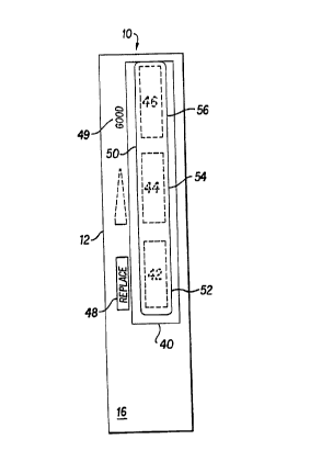
Referring now to FIGS. l and 2, tester lO co~prises a
plurality of rectangular resistive ele~ents 22, 24, 26, and 28
located on the back ~ide 14 of ~uL~r~Le 12. ~uss bars 30 and
31 run along opposite edge~ of the r ~istive element pattern
3, whereby elements 22, 24, 26, and 28 are electrically co~e_Led
in a parallel configuration. Portions 38a and 38b of buss bars
30 and 31, .~F~P ~ively, function as the electrical contact pads
for co~ne~-Lion to the terninal6 of a 9V battery.
~SIJB~;TITUTE SHEE ï
.
A
;''".'',' '. ~ .
~'S '' " ' ' " ' ' ,
' " ~ ' ',
. ~., .
.' "' '' ~ ' ~ '
. .
W092/141~ PCT/US92/Oat~
--5--
2"~?~'3
Substrate 12 can be ~ade from a variety of materials
~ncluding, but not li~ited to, plastic, pap r, cardboard, and
the like. Whichever material i8 ~elected it -~o~l~ be able to
wlthstand the tempe aLu~e of the resi~tive QlQments during the
voltage measurement without shrin~ing, deformlng, charring,
etc.
Resistive elements 22, 24, 26, and 28 can be made from a
variety of resistive materiAls and can ~e Ap~ by a variety
Or different methods. For example, a coating o~ an electrically
resi6tive ink can be coated or printed on the su~L~aLe in the
desired pattern. Suitable resistive material~ include, but are
not limited to, epoxy or ure~hAne ba~ed silver, ~ Arh~n,
or mi~LuL_s thereof. Alternatively, a thin resistive layer can
be applied in the de6ired pattern using any o~ the well known
vacuum deposition t--hn~ -P such as vacuum vapor depositicn,
cathode ~puttering, and the llke. Suitable materials r - -hle
to vacuum deposition include, but are not llmited to, silver,
ni~el, iron, copp~r, car~Qn~ lead, and mi~Lu~es thereof. The
particular choice of material ~ on the resistivity ~e~s~
to achieve t~e desired resistance for a particular size of
SU~ ~ S~E~
. . . .
.
- ~ .
: . , .-: - .
.
W092/141~ PCT/US92/~123
~ 1 Q ~t r~ 6-
resistor. Generally, the size of the resistive ~1 - ts is
llmited by the dimensions of the toster as well a~ the watt
density needo~ to obtain a ~Yr~ -2 from the thermochromic
material ~ir~Rs~ more fully below).
Buss bars 30 and 31 are shap-d to follow th- outside
-ncions of the pattern of resi~tiv- el~ ~nts. The resistance
of each of ele~ents 22, 24, 26, and 28 ~ ~ , in part, on the
distance beL~ecn the .~Q_8~ in~i~e edges of each buss bar.
Thus, for .-~ le, the resistance of element 22 is a function of
the distance ~-t~an the in~ide ~dge Or portion 32a of bus~ bar
30 and th- in~id~ edge of port~on 32b o~ buss bar 31. Bu6s bars
30 and 31 are pr-rerably highly ~v..~ ve so that they do not
contribute --~F~-ably to the o~erall resi-~anc~ o~ the tester.
Any well known cQ~ ~ive lnk c~n be used for the the buss
bars. Examples include, but ~re not limited to metallic inks
comprised o~ silver, CO~L ~ n~ and the like.
Additionally, metal foil can be used i~ it i8 cut to the shape
shown ~n the Figure~ and att~rh~ to the resistive elements
using any of the ~ethod~ of attachment well known to the
artisan.
'. SU~STrrUTE S~EET
.j, . . .
,,,, . : ~ ' '
, ~
. ' ~ ~. ' ' '
:.
.,.. : . : : - ~ :
W092~t41~ PCT/US92/~123
2 ;~ vs 2 ~ ~?
It is preferred that a dielectric coating ~not shown) is
applied over the resistive elements and the bus~ bars with the
exce~Lion of contact pads 38a and 38b. The ~L~ ~e of the
dielectric layer i8 to protect the circuit ~rom phy~ical A- ~ge
a~ well as from ina~ve~-ent ~hort-circuiting of any port~on of
the circuit. Any well known dielectric ink, paint, film, or the
like is suitable for this ~ ose. Example~ include, but are
not limited to, epoxies, acrylics, and ure~h~ne~.
Imprinted on front side 16 of 6ubstrate 12 i5 voltage
;n~io~tion scale 40 which is rectangularly ~h~pe~ and comprises
w~ndc~ 42, 44, and 46. Windows 42, 44, and 46 are co~n~id
with the position o~ resistive e~- Ls 22, 24, and 26,
L~ ively, on the opposite side of su~D~,a~e 12. Voltage
; n~; s~tion scale 40 can be printed, for example, in a dark color
and each window can be printed in ~ bright c~nLL~ting color,
such as yellow.
SUBSTITUTE S~tEET
,
: ,, . ~..................... ,- ' .
', . ,. '
W092/14l~ PCT/US92/~1
~ ;J;)~ -8-
A ther~ochromic layer 50 is located ov~r all three windows
Preferably, layer 50 comprises a ~ omic ink which turns
from opaque to clear above a certain th~ ol~ t~perature,
~r ~he ink preferably has a color at room t-~pe~Lu~e which
i6 similar to the color of scale 40 ~nd ~h~ to clear at a
temperatura above Tr Thus, w~n~ 42, 44, and 46 are
blocked from ~iew at room temperatur- but become visible during
te~ting de~~ ~i ng on the voltage of the battery Generally, a
parti'cular watt density must be re-~he~ in each resistive
element during testing before the tem~e.~Lu~c of the element
Lea~ ~ Tr The watt density i8 a function of th- resistance
Or the resistive _1- -nt, the surrace area of the element and
the voltage applied across th- element The re~i~tance and
surface area of each element become fix-d for a given design 80
that the applied voltage becomes the sole determin~nt of whether
the watt density i8 achieved that is n~- ~' to trigger the
thermochromic ink
While th~_ - h~omic inks are the preferred thermochromic
materials, an alternative, less preferred ~h~ omic material
includes the class of materials known a~ liquid crystals
SUBSTITUT~ SffEET
Wo 92/14144 PCI /US92/00123
Graphics 48 and 49 are printed ~longside scale 40 to
indicate "Replace" and "Good" or any oquivalent message
c~~oerning the condition of the battery being t~ ~e~.
As described, resistive element 28 is not in thermal contact
with the tbermochromic l~yer. The ~ se of resistive element
28 is to act as a shunt and lower the total resistance of the
parallel c -- ~ed resistive elements. Resistive element 28 i5
not a~ne-e~--ry -~ -r~ ~ of the ~.e~~~t invention, h- wc~er it
is desirable to include it when the total resistance of tbe
other "voltage ~n~ic-ting~ resistors is h;~h~r than desired.
For example, the r-sistanc- of ~ typical device ~ d by a 9V
battery is L~t ~r ~bout 50 and 60 ohms 80 tbat this is tbe
desired resistanc- range for a 9V b~ttery tester. If the
re~is~nceF of elenent~ 22, 2~, ~nd 26, _ ~ ~ed in parallel,
give a total re~i~t~nc- Or 1-~ th~n about 60 ohms then element
28 is not ll~e~e~ , if the total resistance of elements
22, 24, and 26 i8 greater th~n ~bout 60 ohms then element 28 is
included to lower the tot~l resi~t~nce of the circuit. The
desired resistance of -1 -r~s 28 i8 determined using Ohm's Law
and the resistance ~alue~ of elQ~ents 22, 24, ~nd 26. This is
~-~c~ese~ more fully below in conne~ion with the description of
a sp~ci~ic ~ ~D -iment.
.
~ SU~ ~E S~tEET
W092/141~ PCT/US92/00123
--10--
;s ~ rt'~ ~)
The principle of operation of test-r lO i~ a~ follows The
te. ;nals of a "fresh" sv battery are ~.~u~1t into contact with
pads 38a and 38b Current flow~ th~g1 bus~ bars 30 and 31 as
well as through resistive elements 22, 24, 26, nnd 28 Element
22 heats up ~astQst hec~ e lt has th- ~alle~t ~ize whoreby it
is first to reach the ne~ ry watt density to trigger the
~he, -- nomic ink A~ view-d fro~ th- front of the tester,
portion 52 of thermochromic layer 50 turns from ~F~ to clear
revea~ling colored window 42 In se~ ial f~ n, resistive
ele~ents 24 and 26 achl-ve th- threshold watt density to trigger
the thermochromic ink wh-reby window 44 foll~d by window 46
are revealed (element 28 al~o heats up but sinc- its function is
not for voltag- ~n~c~tion per se it i8 not di~cus6ed here)
Each resistive eleoent will reach an e~ hrium tem~Ll~Lu~
where the heat ,~r~a~ed by i2R heating is egual to the heat
108t to the ~u~v Atn~ When the ei~ hrium temp~ u~ of a
resistive e1- ~ i8 above Tr the ink which i~ coin~ with
such resistive el ~ will turn from o~r~ e to clear revealing
the colored window beneath Thus, for example, a ~fresh
battery" will cause element~ 22, 24, and 26 to heat sufficiently
so that portions 52, 54, and 56 of thermochromic layer 50 will
turn clear revealing colored wi-~ b'~ 42, 44, 46 on the other
SUBSTlTUTE S~EEl-
... .
''.'~,~ ~ '
. . . .
W092/141~ PCT/VS92/~1
hand, if the battery is near its end-of-life only element 22
will heat sufficiently to reach tho ~pon~e t~mpe ~u.e of the
ink and only window 42 will be r-vealed. At ~ome intermediate
cond~tion of the battery only wi n~ 42 and 44 will be revealed
telling the user that the battery will soon have to be replaced.
The ordering of resistive elements 22, 24, 26 and 28 on
substrate is designed to provide a particular visual effect
during testing. Ac described above, element 22 heats up fastest
d~ring testing followed by elements 24 and 26. This causes a
~, ~ntial visual effect in the the~ - ~romic material on the
front of the tester. ~'~w_~er, other orderings of parallel
col,..e--~ed resistive ele~ents are po~hle for providing
different visual effect~. Further, while shunt resistor 28 i8
shown located immediately beneath contA~ts 38a and 38b it could
be located at the oppoEite end o~ the resistor ~v~ e, or
anywhere else, provided a parallel co\~e_Lion o~ the resistive
elements is maint~i n~ .
SUBSTITUTE S~
-,; i . . .
~' ' ' ' r .
.~. ~ '. ' ',
' , ' ' , '
,,
W092/141~ PCT/US92/~123
O
J
Immediately following is a specific description of a battery
tester for a 9V battery. It is to be lln~ ood, ~ w_~er, that
other design6 are po~ible which are al-o w$thin the scope of
the present invent$on.
The "trigger" voltages for the three resist$ve elements are
~elected as follows. The voltage -'-~- to ~ cAte that a 9V
alkaline battery i8 ~good~ is about 8 volts or ~ore ~ince
~i~c~Arge at, or above, this voltage in~icAtes that the battery
has the majority of its capacity still available. m erefore,
resistive element 26 i- dosignQd to trigger the ther~oc~romic
ink at, or abovo this voltage. The voltage ,-_ to ~ nA i cAte
that th~ battery ~hould be replaced is _bout 5 volts or less
~ince ~t~chArge at, or b-low thi~ volt_ge, ~n~Atos that the
battery is almost completely ~3-harged. There~ore, resistive
element 22 i~ -d to trigger the thermochro~ic ink at about
5 volts. An int-r~ediate voltage which ~ nA ~ rateg that a 9V
battery ha6 had a ma~ority of its cA -~ty removed is about 6.5
volts and this i~ the ~trigger~ value selected for resistive
element 24. The voltages ~ho~ will ~ of cou. e, ! ~- ' on how
~any resistive el ments are used. Additional ~intermediate"
voltages would be ~elected if more than three resistive elements
are used in the circuit.
.~ .
,
SUBST~TUTE S~tEET
.,
;. - . . - , .
~ :'. . '
~ . . -
.
.. , . ~
,,. .:
.',: , .. . .
., .
WOs2/141~ PCT/~S92/OOt~
-13-
2 ~ !) Ul ~ ~ 3
The 6ubstrate is a piece of polye~ter film that i~ 0.005
inch thick, 0.7 inch wide, and 2 jn~hes long. The resistive
elements 22, 24, 26, and 28 each co~pri~e a ~ub~tantially
uniform layer 0.0006 inch thick o~ an epoxy based cA-hon
~heFQ~ Colloids Co., Port ~uron ~h~7~) havin~ a re~istivity
of 300 ohms/square at thi~ thic~ ~9. Element 22 i~ 0.3 inch
wide (the width being the dimension parallel to the short
~i ~ncion of the substrate) and 0.45 inch long: element 24 i6
0.4 inch wide and 0.45 inch long; ele~ent 26 is 0.55 inch wide
and 0.4 inch long; and element 28 is 0.4 inch wide and 0.4S inch
long. These dimensions er.~~L~ that the .~cessAry watt density
will be re~he~ in each resistive element at the predetermined
~trigger" voltages descrlbed above.
Buss bars 30 and 31 are printed on the ~urface and along the
outer edges of the resistive elements using a silver ink
(a~h~sQn Colloids Co.) having a resistivity of 0.01 oh~s/square
at a ~h i C~n~5s of 0.6 mils. Each buss bar is .6 ~ils thick and
.06 inch wide ex~e~ for contact pads 38a and 38b which are
about 0.1 inch wide. The inner edges of buss bar portions 32a
and 32b are 0.2 inch apart, 34a and 34b are 0.3 inch apart, 36a
and 36b are 0.4 inch apart, and contact pads 38a and 38b are
O.35 inch apart.
SIJBSTITUTE SltEET
.. . . . .
.
. . ., ~ .
~. . . - :
WO92/141~ PCT/US92/~1
-14-
As mentioned previously, the resistance of the resistive
elements depends, in part, on the di~tance bct~acn the 0~03e~
inside edges of the buss bars attached to each resistive
element. The resi~tance of eleoent 22 i- about 150 ohm~, the
resistance of element 24 is about 250 0~08, th- resistance of
element 26 ~s about 325 ohms, and the resistance of element 28
i5 about 250 ohms. According to Ohm's ~aw these resistors,
conre~-Led in parallel, have a total re~i~tance of about 55
ohms.. The effect of including element 28 in the circuit is
evident by calculating what the total resistance would be if
only elements 22, 24, and 26 were con~ Led in parallel. That
calculation gives a value of about 70 ohms. Thus, including
~1 f - - L 28 in the circu~t lowers the ovorall resisLah~c to a
value which i~ closer to that of an r_t~l device. It is
possible that by choos~g a different resistive ~aterial the
resistance of ele~ent~ 22, 24, and 26 could be eh~ 0 that
shunt resistor 28 is not r.ea - . Y ~.el, thi~ can be difficult
to achieve exactly with three resi~tor6. Greater flexibility is
provided by using a shunt resistor to "fine tune" the total
resistance after ele~ents 22, 24, and 26 are designed.
SUBSTITI ITE St tEEr
.
.Y . ......
:: .
~ , :
: . .
WO92/141~ PCT/US92/~123
-15-
~ I 'J'~ 3
The thermochromic ink used in this exa3ple i~ Type 47 made
by Matsui Internation~l co , Inc which h~ a .~
temperature, Tr~ of about 47 C The watt den~ity -~'~d in
each of the above described resistivQ elements to reach the
L. ,~ temperature of this ink i- _bout l 5 watts/in2
A dielectric layer of an acrylic ~'~50~ Colloids Co )
0 0006 inch thick i8 applied over the r sistivo eloments and
buss bars with the ~x~o~Lion of contact pads 38a and 38b
The front surSace 16 of sub~trate 12 is fir-t printed over
with a green ha~ ~J.~d color A bright yellow stripe is
printed onto the green ~- ~J~VU d _nd the voltage i n~ication
scale 40 co~prising w~nd~__ 42, 44, and 46 is printed in black
over the yellow ~tripe such that yellow is only visible h.~uyl.
said wi~ As ~ t ~bove, wi-'~ 42, 44, and 46 are
positioned so that they ar- co~nc~d-- t with resistive elements
22, 24, and 25 Gr~r~c~ ~8 and ~9 are printed along scale 40
The above descr~bed t-ster can be used as _ rree g~an~i ng
tester or it c~n b- ~ade an integr_l p_rt of the r~ e used
for the displ_y ~nd sale of the batteries Sincç the total
L flowing th.~agh t~e tester during t-sting is split among
four resistors the heating proble~ Acsocj~ted with a single
wedge sh~re~ element is avoided
SUBSTITUTE SHC~
.
., . -
~'.. . . . . , ~
' ~; : ~ '
. .
.
W092/14~4~ PCT/US~2/OOt23
~ 16-
While the above d-~cribed '~ L i~ pr~rerred, there is
another, althovgh less pre~erred, ~cbodiment vhich al80 uses
parallel ~: - Led re~istive el~m-ntG Thi~ ~ bodi~ent e~ploys
r-si~tiv~ element~ having the 8~0~ rL-r ln~d resi~a ce and
a di~ferent ~- - h- o~ic ~aterial in th-r~al contact with each
rQsistive ele~ent For exampl-, a~sume ~leuent~ 22, 24, and 26
all have the s~me resistance Portlon 52 oS th-rmochromic layer
50 would compri-e a theroochromic ink which would .~Y~--' to the
watt density reculting rrO~ applying 5 volts acro~s the
re~istive elements Portion 54 o~ omic layer 50 would
oomprise a ~ dlr~erent th- D ochromlc lnk whlch would
.~ ~ ' to only ~ higher watt den~ity r-~ulting ~ro~ applying
6 5 volt~ across the reslstive ~leoents Port~on 56 of
theroochromic lay-r 50 would co~pri~e a third dirre._n~
thermochromic ink which would r-spond to only a watt density
r sulting rrO applying 8 volt~ the r ~i~tlve ~lements
Thus, th~ s~ce voltage ~n~c~tion would be ~ d as with
using the pre~erred embodlnent A di~n~a Lage to this less
preferred embodi~ent $8 that two additional ~anuracturing steps
would be reguired ~or applylng the oecon~ and thlrd
thermochromic ink~
SUBSTlTlJlE S~tEET
.. ~,' ' - ~ .
,
. - . ..
W092/141~ PCT/~S92/~123
2 1 ~ '3 ~ ~i 3~
While the above described design relates to a tester for ~V
batteries, the present invention can be used for testers
designed for cylindrical 1.5V cells ~uch a D, C, AA, and AAA
~izes. Materials other than those de~cribed in the Fpe~i fic
example can be used to fabricat- te~ter~ within the scope of the
~ nt invention. The Fp~clfic exa~ple is for $11ustrative
purposes only and is not intr~ to li~it the scope of the
invention as claimed.
.
SUB~TITUTE ~tEE~
:, '
.. . .
- . ' ' ' , .. . . .