Note: Descriptions are shown in the official language in which they were submitted.
BACKGROUND OF THE INVENTION
1 Field of the Invention
2 This invention relates to a circuit for measuring the
3 conductivity of a solution disposed between two electrodes. More
4 particularly, this invention relates to circuits for accurately
measuring the conductivities of solutions varying over several
6 orders of magnitude, wherein inherent sources of parallel and
7 series capacitance are accurately compensated for.
8 Description of the Prior Art
9 There are many applications wherein it is desired to measure
the electric conductivity of a solution. The conductivity of a
11 solution is a measure of the dissolved ionic content of the
12 solution. In Iow conductivity solutions, ranging from ultra-pure
13 water used in semi-conductor and pharmaceutical manufacturing to
14 power plant cooling water and potable water, the conductivity is
measured as an indication of ionic impurities. In higher
16 conductivity solutions, such as process chemicals and the like,
17 conductivity is often measured to monitor and control the addition
18 of ionic additives. In each of these applications there is a
19 distinct need for apparatus and methods to accurately measure the
conductivity of water. Measurements of the conductivity of
21 solutions are relevant in, many other industries and applications.
22 The conductivity of a solution can be determined by measuring
23 its electrical resistance. Due to the nature of ionic solutions,
24 however, measuring this resistance with do current will cause ion
migration that can substantially affect the measurement. For this
1 reason,. ac current is generally employed, at a voltage low enough
2 and a frequency high enough to not affect the solution during the
3 measurement.
4 The volume resistivity or simply the 'resistivity' of a
solution is defined as the resistance of one cubic centimeter of
6 the solution at a specific temperature. The units of resi.stivity
7 are ohm-cm (S2-cm), kiiohm-cm (KS2-cm), or megohm-cm (MS2-cm).
8 Resistivity may be measured directly by applying an alternating
9 current I~ through the cell and measuring the resulting voltage
drop V~ across the electrodes. The resistivity p is then:
11 p = V~/KI
12 where: p is the solution resistivity, in S2-cm
13 I~ is the current applied through the cell, in amperes
14 V~ is the voltage measured across the cell, in volts
K is the cell constant.
16 The volume conductivity of a solution, known as 'specific
also
17 conductance', is defined as inverse of resistance of
the the one
18 cubic centimeter of the solutionat a specifictemperature.
The
19 units of specific conductivity known as Seimens)
are mho/cm (also
and pmho/cm (~rSeimens, or uS).Conductivity may be measured
21 directly by applying an alternating
voltage source Va across the
22 cell and measuring the resultingcurrent I
thereon. The
specific
~
23 conductance a is then:
3
2~~a~~~i
1 Q = KI~/v
2 where: a is the specific conductance, in mho/cm
3 V~ is the voltage applied across the cell, in volts
4 I~ is the measured current through the cell, in amperes
K is the cell constant.
6 In either case, the basic parameter measured is the actual
7 resistance of the solution, RX = V~/I~. Accurate measurement of RX
8 is complicated by the presence of a parallel capacitance CP across
9 the cell and a series capacitance CX formed at the solution-cell
interfaces.
11 Fig. 1 depicts a approximate equivalent circuit of the
12 solution-electrode interface. The solution resistance of interest
13 is depicted as RX. Each electrode-solution interface forms an
14 imperfect 'double-layer' capacitance Ca with an effective series
resistance R~ and an effective leakage resistance Rd. Additionally,
16 a capacitance C9 is formed by the surface area of the electrodes I4
17 and 16 separated by the solution, acting as a dielectric.
18 Fig. 2 depicts a simplified equivalent circuit of the cell.
19 The circuit parameter of analytical interest is RX, the resistance
of the solution, primarily responsive to the ions in the solution.
21 Cp is the total effective parallel capacitance existing between the
22, two electrodes, including any cable capacitance. The value of Cp
23 is substantially proportional to the area of the electrodes .and
24 inversely proportional to the separation of the electrodes. Cp
typically varies from less than 100 gf to over 1000 pf depending on
4
1 cell geometry. Cx is the total capacitance in series with RX,
2 approximately equal to Cd/2, and is again a function of cell
3 geometry, generally increasing with increasing electrode surface
4 area. CX typically ranges from 1 to 10 uf.
Fig. 3 is a graph of the actual resistance RX (actual) of the
6 solution in the cell versus the resistance observed RX (meas), that
7 is, if no compensation is made for the contributions of Cx and Cp.
8 As RX (actual) gets lower, i.e., in a solution containing larger
9 numbers of ions, the impedance of CX becomes a larger proportion of
Rx (actual) and introduces an error indicated on Fig. 3 as "CX
1I error". As RX (actual) gets higher, in less-ionic solutions, the
12 parallel impedance of Cp progressively reduces the measured
13 impedance and introduces the error indicated as "CE error".
14 Fig. 4 is a graph of the conductivity ax = 1/RX of the sample
in the cell, indicating the deviation of the conductivity ox
1,6 (actual) from the value ax (meas) of the conductivity as measured.
17 Since ax as indicated is equal to 1/Rx, the effects of the parallel
18 and series capacitances Cp and Cx are inverted as shown.
19 Thus a circuit for adequately measuring conductivities of
solutions over a wide range of conductivity values must adequately
21 take into account and eliminate both Cp and Cx as sources of
22 inaccuracy.
23 An early method used in the prior art to measure solution
24 conductance employs an AC conductance bridge, where various
reactance are added to arms of the bridge to compensate CX, Cp or
5
I both. This method has been shown to be effective but is generally
2 slow and requires manual operation.
3 Digital impedance meters are available (Model 254, Electro
4 Scientific Industries, Inc.) that employ sine-wave excitation and
synchronous phase angle detection to separate the conductance due
6 to reactive components. Again, this method is effective but is
7 expensive and relatively slow, and cannot be effectively automated,
8 as would be desired.
9 It is desirable to use a square-wave excitation signal to
drive the cell, that is, to apply a square-wave signal to one
1I electrode of the sample cell, and measure the current through the
12 cell to determine the resistivity of the solution, due to the ease
13 with which precision amplitude square-waves can be generated.
14 However, the presence of Cp and CX can lead to significant linearity
errors if not actively compensated for. Applicant's prior U.S.
16 Patent No. 4,683,435 addresses in detail one approach to
17 compensating some of these errors while using a square-wave drive
18 signal. The present invention reflects additional understanding of
19 the problems inherent in measuring the conductivity of a solution
confined between two electrodes in a cell and presents additional
21 and improved solutions thereto.
22 OBJECTS AND SUMMARY OF THE INVENTION
23 It is therefore an object of the invention to provide a
24 circuit and methods for.measuring the conductivity of solutions
6
21~~~~~
1 that minimizes the effects of series and parallel capacitance
2 inherent in cells containing samples of such solutions.
3 The above object of the invention and others which will appear
4 as the discussion below proceeds are satisfied by the present
invention, which comprises circuits and methods for accurately
6 measuring the conductivity of solutions of widely varying
7 conductivities. More particularly, it has. been realized by the
8 present inventor that entirely different techniques are desirably
9 employed for compensating for the parallel and series capacitances
Cp and CX, due principally to their relatively large disparity in
11 values; Cp is normally orders of magnitude smaller than CX. It is
12 an object of the invention to provide such different techniques.
13 As noted, it is desired to measure the conductivity of the
14 solution by measuring current flowing through the solution
responsive to an applied square-wave drive signal. The effect of
16 the presence of Cp and CX is to distort the square-wave current
17 signal due to charge being stored over time on the capacitances
18 represented by Cp and Cx.
19 It has been realized by the present inventor that if the
parallel capacitance represented by Cp is fully charged prior to.
21 sampling the conductivity, the presence of Cp and the error
22 produced by Cp will be fully compensated. The rate of charge of Cp
23 is a function of the total equivalent series resistance through
24 which the drive signal applied to the cell passes. This series
resistance is normally the drive source resistance in parallel with
26 the solution resistance RX. However, it has been realized by the
7
1 present inventor that under some circumstances, the input
2 resistance of the current-to-voltage converter typically used to
3 measure the resistance of the cell can contribute to the series
4 resistance. More particularly, when the feedback resistance Rt of
a feedback loop employed as part of typical current-to-voltage
6 converter is high enough to provide sufficient gain at low values
7 of the solution conductivity, the converter will clip during
8 charging of Cp, open the feedback loop, and add Rf to the series
9 resistance.
Accordingly, it is an object of the invention to set Rr to a
11 value low enough to allow CP to charge fully prior to sampling the
12 conductivity of the cell, and thereafter controllably vary Rr such
13 that the gain of the feedback loop is appropriate for measurement
14 of the solution conductivity.
The rate of charge of the series capacitance Cx is a function
16 of the solution resistance RX only. The effect of Cx is to reduce
17 the voltage applied across RX, thus producing an error in the
18 conductivity measurement. While this error can not be easily
19 eliminated, it has been realized that due to the typically large
value of Cx, the voltage Cx reaches and thus the error Cx produces
21 can be reduced to a negligible level by controlling the amount of
22 time CX can charge prior to sampling the conductivity, responsive
23 to the solution resistance RX~.
24 It is therefore an object of the invention to provide a
circuit for measuring the conductivity of a solution employing a
26 bipolar drive signal, wherein the frequency of the drive signal is
8
1 controllably varied responsive to the order of magnitude of the
2 solution resistance, whereby the voltage reached by CX is
3 negligibly small.
4 It is a more specific object of the invention to provide a
circuit for measuring the conductivity of a solution wherein the
6 parallel capacitance Cp is fully charged prior to making the
7 conductivity measurement, so that Cp does not distort the
8 measurement, and. wherein the distortion introduced by CX is
9 minimized by limiting the effect of CX at the time the measurement
is made.
11 More specifically, a typical current-to-voltage converter
12 employs an op-amp having a feedback resistor Rt connected between
13 its inverting (negative) input and output terminals. The
14 noninverting (positive) input of the op-amp is connected to a
circuit common potential, i.e., ground. In this standard
16 configuration, the negative input becomes a virtual ground,
17 exhibiting essentially zero input resistance as long as the
18 feedback loop is closed. However, if the current into the negative
19 input terminal exceeds the output voltage swing capability of the
op-amp for a given feedback resistance, the op-amp response clips,
21 the feedback loop opens and the feedback resistance R! becomes the
22 effective input resistance. Another constraint on the feedback
23 resistance Rt in the current to voltage converter feedback loop is
24 that R= must be large enough to produce the required gain during
measurement of the resistance of the cell. For example, Rr
9
~~~~4~
1 typically should be 1 MS2 or more for measuring the conductivity of
2 low-conductivity, high resistivity ultrapure water solutions.
3 According to one object of the invention, it is desired to
4 maintain the total drive source resistance at a low enough level to
charge Cp in a relatively short period of time, at the beginning of
6 each half-cycle of the drive signal, so as to prevent charge
7 accumulation by C~ from interfering with subsequent measurement of
8 the current through the cell. If Rt is high, e.g., 100kSt or more,
9 during charging of Cp, the op-amp will not be capable of supplying
sufficient feedback current, and will clip. Therefore, according
11 to one aspect of the present invention, Rf is reduced to a level
12 low enough to cause that Cp is fully charged early in each half
13 cycle of the drive signal. Rf is then increased to a value
14 corresponding generally to the range of, the resistance of the cell,
in order to provide sufficient gain in the feedback loop to measure
16 the current flowing through the cell during a latter portion of the
17 same half-cycle. Conveniently, several discrete feedback
18 resistances Rio - Rfn are provided to define a like number of gain
19 ranges. After Cp is fully charged, Cp no longer affects the current
flowing through the cell, and thus the error produced by Cp.is
21 effectively compensated for.
22 The rate of charge of the series capacitance Cx is
23 proportional to the solution resistance RX. CX produces an error
24 in the measured current by reducing the voltage applied across Rx
by the amount that Cx is allowed to charge in each half-cycle
26 before the measurement is 'made. With a fixed frequency drive
2~~~-~~
1 signal, the error due to CX would. increase as the solution
2 resistance decreases. Therefore, according to another aspect of
3 the present invention, the period T of the bipolar drive signal is
4 decreased as the solution resistance decreases, so as to limit the
voltage reached by Cx to within a predefined accuracy requirement.
6 In practice, this is accomplished by using separate drive
? frequencies for each gain range.
8 The inventor has further realized that by varying the period
9 T of the drive signal responsive .to the solution resistance,
maximum filtration of extraneous random noise can be readily
11 achieved. More specifically, the sensitivity of the current-to
"12 voltage converter to electrical noise is proportional to Rf, i.e.,
13 to the gain of the current-to-voltage converter. As noted, to
14 achieve a wide range of conductance measurements, it is desirable
to make Rt selectible for several gain ranges, e.g., by providing
16 several selectible feedback resistances Rio - Rrn. Furthermore, if
1? a feedback capacitor Cr is added to filter noise, it is
18 advantageous to place the feedback capacitor Ct across the op-amp
19 itself rather than across each of the resistances Rfn, in order to
keep the loop stable during gain switching. With a fixed frequency
21 drive signal, Cf would be required to be small enough to be charged
22 fully with the Largest R! before the conductivity is sampled at the
23 end of each half-cycle. Such a small Cf value would allow maximum
24 filtering only on the highest gain range. Therefore, according to
a further aspect of the present invention, the filtering is made
26 constant across all the gain ranges, i.e., the voltage that Cr
11
CA 02100436 2003-09-09
reaches at the sample time is is made essentially constant, by varying the
period
T of the drive signal in proportion to the selected value of Rf. Since C, is
the same
for all of the R,'s, the period T is effectively varied in proportion to the
time constant
R,~*C,. It will be noted that variation of T to thus ensure Cf is fully
charged is the
same solution as described above for compensating the effects of CX, thus
simultaneously providing a simple and elegant solution to two problems not
solved
by the prior art.
It is desired to employ the circuit of the invention to monitor the
conductivity
of a solution juxtaposed to a source of periodic noise. For example, a mercury
vapor lamp driven by a switching power supply may be disposed near the
conductivity cell, in order to oxidize organic compounds in the solution to
carbon
dioxide. The circuit of the invention is desirably used to measure the
conductivity
prior to, during, and after oxidation. The amount of such organic compounds in
the
solution can then be calculated responsive to the change in the solution's
conductivity. Noise from the lamp drive circuit interferes with the
measurement.
According to a further aspect of the invention, the noise can be minimized if
the
period of the bipolar cell drive signal is an integral multiple of the period
of the lamp
drive signal; in this way, the noise is averaged to zero.
In accordance with one aspect of the invention there is provided a method
2 0 for measuring the conductivity of a solution disposed between two
electrodes, such
that an error in the measurement produced by the conductance of a parallel
capacitance CP across the electrodes is minimized, comprising the steps of
applying
a biopolar square wave drive signal having a period T across the electrodes
through a series resistance RS; changing CP during a first portion t~ of each
half
2 5 cycle T/2 of the bipolar drive signal, while maintaining RS at a
sufficiently small value
during t~ to allow Cp to charge to its maximum value during t~; measuring the
current
conducted between the electrodes during a latter sampling time portion is of
each
half cycle T/2 of the bipolar drive signal T; and determining the conductivity
of the
solution responsive to the current measured in the measuring step.
12
CA 02100436 2003-09-09
In accordance with a second aspect of the invention there is provided an
apparatus for measuring the conductivity of a solution comprising of a sample
cell
including two electrodes for receiving a sample of the solution, which
solution
exhibits a capacitance across the electrodes; means for applying a bipolar
square
wave drive signal having a period T between one electrode, and a circuit
common
potential; a summing junction to which the other electrode is connected;
feedback
means (Rf) for maintaining the summing junction at the circuit common
potential;
means for measuring the current between the electrodes; and means for
determining the conductivity of the solution responsive to the current
measured;
1 o characterised in that means are provided for charging the capacitance to
its
maximum value during a first portion, t~, of each half cycle T/2 of the
bipolar drive
signal; and means are provided for conducting the current measuring during a
later
sampling time portion of each half cycle T/2; the apparatus additionally
including
a network of selectable discrete feedback resistors R,o - R,~ as the feedback
means,
Rfo being of sufficient low resistance to ensure the capacitance is charged to
its
maximum value during t~; means for selecting R,o during t~; and means for
selecting
between the resistors R,o - R,n during each half cycle after t~ to determine
the circuit
gain.
The above objects and summary statements will now be described in greater
detail having regard to the drawings and description which follow.
13
CA 02100436 2003-09-09
BRIEF DESCRIPTION OF THE DRAWINGS
In the drawings which illustrate embodiments of the invention:
Fig. 1 is an approximate circuit diagram of a solution the conductance of
which is to be measured;
Fig. 2 shows schematically a simplified equivalent circuit diagram,
illustrating the series resistance RX, the series capacitance Cx, and the
parallel
capacitance Cp of the solution of Fig. 1;
Fig. 3 shows a graph of actual resistance of a solution in a cell versus the
measured resistance;
1 o Fig. 4 is a similar diagram showing the actual conductivity of the
solution
in the cell versus the measured conductivity;
14
1 Fig. 5 shows a typical bipolar square wave drive signal as a
2 function of time;
3 Fig. 6 shows the current passing through a solution in a cell
4 responsive to the drive signal of Fig. 5, as a function of time;
Fig. 7 is a simplified block diagram of one circuit for
6 measuring the conductivity of a solution in a cell according to the
7 invention;
8 Fig. 8 is a timing diagram showing the drive signal applied to
9 the cell and the current through the cell, and identifying certain
periods during the bipolar drive signal at which various control
I1 actions are taken;
12 Fig. 9 is a graph showing the drive signal as a function of
13 time, together with a further graph showing the charging of the
14 series capacitance Cx as a function of time;
Fig. 10 is a detailed block diagram of one circuit for
I6 measuring the conductivity of a solution in a cell according to the
17 invention;
18 Fig. 11 is a detailed schematic diagram showing the circuit of
19 Fig. l0 more fully;
Fig. 12, comprising Figs. 12(a) through (f), shows certain
21 signals occurring in operation of the circuit of Figs. I0 and 11 in
22 a mode of operation suitable for measuring the conductivity of a
23 relatively highly conductive solution;
24 Fig. 13, comprising Figs. 13(a) through (f), is a diagram
similar to Fig. 12 illustrating the operation of the circuit of
1 Figs . 10 and 11 as used to measure the conductivity of solutions of
2 relatively lesser conductivity;
3 Fig. 14 is a block diagram of a circuit of a further
4 embodiment of the invention for measuring the conductivity of a
solution in a cell;
6 Fig. 15 includes a diagram of a bipolar drive signal as a
7 function of time (Fig. 15(a)), and a diagram of the output signal
8 of an op-amp in the circuit of Fig. 14 as a function of time (Fig.
9 15(b)); and
Fig. 16 is a cross-sectional view of a cell in connection with
1I which the circuits of the invention may be useful, together with a
12 block diagram of a complete instrument for measurement of the
13 organic carbon content of water employing the circuit of the
14 invention.
DESCRIPTION OF THE PREFERRED EMBODIMENTS
16 Fig. 1, as indicated above, shows an approximate equivalent
17 circuit of a cell including electrodes 14 and 16 between which a
18 solution the conductivity of which is to be measured is disposed.
19 The equivalent circuit includes "double-layer" capacitances Cd,
typically 1-lOUF, formed by the electrode-solution interfaces.
21' These capacitors exhibit an equivalent series resistances R~ and
22 leakage resistances Rd. R~ may be on the order of 3n while Rd is
23 typically 200kS2. The equivalent circuit also includes the cell
24 capacitance Cg, on the order of hundreds of pf,. due to the presence
of the dielectric solution between the electrodes 14 and 16. The
16
~~~~43
1 solution resistance, RX, may vary widely, between <Ik52 and 100MS2,
2 depending on the solution, the cell design, temperature and other
3 variables.
4 Fig. 2 illustrates a simplified equivalent circuit. The
solution in the cell may be represented by a series resistance Rx
6 to be measured, equal to the resistivity p of the solution times
7 the cell~constant K, or equivalently equal to K. divided by the
8 conductivity a, a series capacitance CX essentially equal to Cd/2,
9 and a parallel capacitance CP substantially equal to C9. CP is
IO effectively the capacitance existing by virtue of the opposition of
11 electrodes 14 and 16 with the dielectric solution therebetween, RX
12 is the resistance of the solution, varying in accordance with its
13 ionic content, and Cx is the series capacitance arising due to the
14 presence of dual polarized layers of ions near the electrodes.
As also indicated above, Figs . 3 and 4 show that the error due
16 to Cp primarily affects conductivity measurement of waters of high
17 resistivity, that is, of low conductivity, while conversely the CX
18 error becomes significant in connection with solutions of low
19 resistivity or high conductivity. As noted, it is an object of the
invention to separately and appropriately compensate these sources
21 of measurement error.
22 Fig. 5 shows a typical bipolar square-wave drive signal Vdriva
23 used to excite the cell according to the circuit of the invention.
24 Fig. 6 shows the current I~el~ flowing through the cell responsive
to Vdrive~ that is, without the improvement according to the
26 invention. The characteristic exponential shape distorting the
17
~vi~ ~~
1 square-wave shape of I~exl during each half of the bipolar drive
2 signal is due to the presence of CP. That is, at the beginning of
3 each half of the bipolar drive signal Vdrl~e, CP draws substantial
4 current, so that the output current I~exl is distorted until Cp
becomes substantially fully charged. Thereafter, the current
6 through the cell I~Bxx is essentially. proportional to the total
7 series resistance Rg.
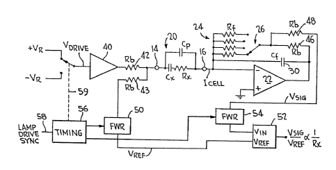
8 Fig. 7 shows a simplified block diagram of a circuit according
9 to one embodiment of the invention for measuring the conductivity
of a solution disposed between electrodes 14 and 16 in a cell
11 indicated generally at 20. Bipolar square-wave drive signal Vd
12 of period T is applied to one electrode 14 of the cell 20. The
13 other electrode 16 of the cell 20 is connected to the inverting
14 (negative) input of an op-amp 22. A network of selectable feedback
resistances Rto - Rtn 24 is provided with a switchable connection 26
16 such that the effective value of feedback resistance R~ between the
17 output and inverting terminals of op-amp 22 can be selected. The
18 non-inverting terminal of the op-amp is grounded, that is, is
19 connected to circuit common potential. As is well known, an op-amp
22 connected as shown will produce whatever output voltage (within
21 its output voltage swing capability) is needed to drive the inputs
22 to equality. This produces a virtual ground at the inverting input
23 and serves as a zero-voltage current sensing point. Accordingly,
24 the output voltage Vslg will be proportional to I~axx% more
specifically, the op-amp output voltage Vei9 will be essentially
18
2~~~~~J
1 equal to the current flowing out of this node times the feedback
2 resistance Rf.
3 According to one aspect of the invention, one of the
4 resistances Rrn is designed to be low enough to substantially fully
charge the parallel capacitance CP existing in the cell during an
6 initial charging portion t~ of each half T/2 of the bipolar drive
7 signal. See Fig. 8. This value of the feedback resistance may
8 coincide with the feedback resistance used to provide the desired
9 op-amp gain in measurement of the conductivity of solutions in the
highest conductivity range. If Rr is chosen appropriately, as
11 indicated, the current through the call due to the presence of CP
12 reaches its final value during a charge period t~, ending
13 relatively early in each half-cycle. If the current Dell is sampled
14 during a sampling period t. at the end of each half-cycle T/Z of
the bipolar drive signal, the distortion caused by Cp is minimized.
16 In practice, a filter capacitor Cr 30 is placed across the
17 noninverting input and output terminals of the op-amp 22, to filter
18 noise. It is advantageous to place Cr across the op-amp itself
19 instead of across each feedback resistor Rfn in order to stabilize
the loop during range switching. As noted, Rt is selected so that
21 Cp is substantially fully charged during an initial charge period
22 ta. At this time, Vsi9 (again, the output voltage, proportional to
23 the current Dell through the cell) is near zero. After Cp is fully
24 charged, Dell increases exponentially with a time constant C!*Rr due
to the gradual charging of filter capacitor Cr. The time constant
26 must be such that Icaal reaches substantially its final value towards
19
1 the end of each half cycle, that is, before the sampling time t0.
2 Tf T is made to vary proportionally with Rt, the total charge on Cf,
3 a function of T/2 multiplied by the time constant Rf*Ct, will remain
4 constant across the ranges provided by the resistances Rrn to allow
control of the circuit gain, as explained above. Again, the
6 current through the cell is sampled only at a sampling time to
7 towards the end of each half cycle T/2, to ensure the current is
8 sampled only after both Cp and Ct have been substantially fully
9 charged. In this way, the value measured for the current is
representative of the resistance of the solution RX in the cell.
11 As noted, the rate of charge of CP varies in accordance with
12 the total series resistance RS experienced by Vd=1~a~ RS includes
13 both RX and Rr when the loop is open: The correct rate of charge
14 of Cp is controlled by control of Rr in accordance with Rx.
Therefore, as indicated in Fig. 7, the feedback resistance Rt is
16 selectible from a series of values typically varying over four
17 decades to ensure that the total series resistance R$ experienced
18 during the initial charging period t~ is sufficiently low to ensure
19 that Cp is substantially fully charged during t~. Thereafter, the
feedback resistance Rt may be increased to a higher value to ensure
21 the gain of the op-amp circuit is suitably responsive to Rx, as
22 above; that is, Rr is selected to control the desired gain
23 corresponding to the order of magnitude of RX, so that tha op-amp's
24 output voltage is not clipped, as would occur if Rx « Rr, and so
the output voltage Vai9 is of the same order of magnitude as V~l
2~.~~~~~~
1 It will be recalled from the discussion above that a series
2 capacitance CX is also in series with the cell resistance Rx. As
3 indicated above, CX is on the order of uf, as compared to Cp, on the
4 order of pf. The method of compensation of CP employed according
to the invention, that is, fully charging Cp, is not satisfactory
6 for compensating CX, as the error is proportional to the charge of
7 CX. However, it has been realized that the time constant of
8 charging of CX is CXRX; that is, variation in Rf does not affect the
9 rate of charge of Cx. The total voltage on CX at the end of each
half-cycle is:
-T/2RxCX'
Vdzive ~ ~- -
11 Therefore, according to another aspect of the invention, the
12 frequency of the bipolar drive signal is controlled responsive to
13 the range of Rx to ensure that Cx only charges very slightly during
14 T/2. The distortion contributed by Cx may thereby be controlled to
be beneath the accuracy target of the instrument. In one
16 embodiment of the present invention, .O1% accuracy is required; the
17 contribution of CX to distortion in the current through the cell
18 can readily be controlled to be less than this value. In practice
19 of the invention, by controlling T, as above, responsive to the
range of RX, the distortion introduced by CX is reduced to a
21 negligible level and is disregarded. Fig. 9 shows an exaggerated
22 illustration of the voltage across CX as a function of time.
21
1 Fig. 10 shows a detailed block diagram of a circuit according
2 to the invention for measuring the conductivity of a solution in a
3 cell corresponding to the simplified block diagram of Fig. 7. Fig.
4 11 shows a schematic diagram of the circuit of Fig. 10, with the
components identified identically where appropriate. Figs. 12 (a)
6 - (f) are timing diagrams illustrating the operation of certain
7 elements of the circuit of Figs. 10 and 11 as employed when the
8 conductivity of the solution is high. Figs. 13 (a) - (f) are
9 similar timing diagrams illustrating ogeration of the circuit when
IO the conductivity of the solution is low, e.g., when the solution is
11 ultrapure water or a similarly highly resistive solution.
12 Referring now to Fig. 10, the bipolar drive signal Vdri~e is
13 generated by switching between positive and negative sources of
14 supply voltage VR. The drive signal Vdrs~e is buffered in a buffer
40. The signal is then passed through a solid state mode switch 74
16 having switch resistances Rb indicated at 42 and 43, for purposes
17 discussed below, and then is supplied to one electrode 14 of a cell
18 20. Cell 20 effectively comprises a series capacitance CX, a
19 series resistance Rx and a parallel capacitance Cp, all as discussed
above.
21 The output current Dell flowing through the cell 20 is applied
22 from electrode 16 to the inverting (negative) input of an op-amp
23 22. A.filter capacitor Cr 30 and a resistor network 24 for
24 permitting switched control of the value of feedback resistance R~
are connected between the inverting and output,terminals of op-amp
26 22 in feedback configuration. Solid-state range switch 26 controls
22
1 the operation of the feedback resistor network 24, and includes
switch resistances Rb indicated at 46 and 48, compensated for in a
3 manner discussed below.
4 As indicated above, input signal Vdri~e is applied to the cell
20, from which output current I~e~l is supplied to op-amp 22. As
6 noted, op-amp 22 supplies output current as needed to drive the
7 input terminals to equality. Since the positive input terminal is
8 grounded, the negative input terminal is a virtual ground, and the
9 feedback current supplied by the op-amp is the inverse of I~em The
value of Rf selected by range switch 26 at any given time controls
11 the total series resistance Rg experienced by current passing
12 through the cell, that is, Rf controls the feedback circuit gain.
13 Thus, where the solution resistance Rx is high, e. g. , 1 mS~, the
14 switched resistor network 24 is operated so that a low feedback
resistance, e.g., lkSt is in circuit during an initial charge
16 portion t~ of each half of the bipolar drive signal. This ensures
17 that the parallel capacitance Cp is fully charged during t~.
18 Thereafter, the switched resistor network 24 is controlled to vary
19 Rr such that the total series resistance RS and hence the circuit
gain are appropriate to ensure that the filter capacitor CF is
21 fully charged during the remainder of each half T/2 of the bipolar
22 drive signal Vdri~g (see Fig. 8) prior to the sampling time te.
23 In order to accurately sample the signal, the drive signal
24 vd=i~e is full-wave rectified in a full-wave rectifier (FWR) 50 and
supplied as the reference input Vrar to a ratiometric analog-to-
26 digital converter (ADC) 52. The signal input Vin to the ADC 52 is
27 the output voltage signal Ve3g from op-amp 22, having been similarly
23
22~~4~~
1 full-wave rectified by a second full-wave rectifier 54. The output
2 of the ADC 52 is a binary value proportional to Vin divided by Vraf,
3 or in this case, to the absolute value of Veig divided by the
4 absolute value of Vdli~e. Since VAig is proportional to I~B~l, the
output of analog-to-digital converter 52 is accordingly
6 proportional to the conductance of the solution in the cell.
7 The output signal from the cell V9lg is full-wave rectified
8 prior to the ADC 52 so that any do bias in the circuit, e.g., due
9 to cell chemistry, ~op-amp bias current and the like is
automatically eliminated. The op-amp bias current through the
11 feedback resistance Rf impresses a do bias in the output signal
12 from the op-amp. This bias current may be of either polarity, but
13 is of the same sign during both halves of the bipolar output
14 signal. Therefore, when the two halves of the bipolar output
signal are summed in rectification, the biases will cancel out.
16 Similar do bias error in the drive signal Vdri~e due to switch
17~ resistance 42, or to other sources, is eliminated in full-wave
18 rectifier 50.
19 In the preferred embodiment, and as discussed below in
connection with Fig. 11, full-wave rectifier (FWR) circuits 50 and
21 54 are implemented using flying capacitor techniques, to provide a
22 high signal-to-noise ratio in the output signal. The flying
23 capacitor FWR circuits are controlled by a timing network 56. One
24 use of the circuit of the invention is in instruments for measuring
the organic carbon content of water. In such instruments, the cell
26 is desirably operated in conjunction to a source of ultraviolet
24
1 radiation driven by a high frequency signal to convert any organic
2 material in the solution to carbon. In such instruments, timing
3 network 56 is operated in synchronization with the signal driving
4 the ultraviolet lamp, as indicated at 58. The cell drive signal
Vdriva is similarly synchronized to the lamp 'drive signal, as
6 indicated at 59. More specifically, the period of the full-wave
7 rectifier circuit control signals and the cell drive signal are
8 controlled to be integral multiples of the period of the Iamp drive
9 signal. By thus driving the flying capacitor full-wave rectifier
circuits and the bipolar call drive signal VdriVe in synchronization
11 with the lamp, the noise added to the output signal due to the
12 juxtaposition of the cell to the lamp is averaged over an integral
13 multiple of cycles of the lamp drive signal frequency, thus
14 canceling noise due to the lamp drive signal from the output signal
from the cell. In this use of the circuit of the invention, W
16 radiation from the lamp falls on the electrodes of the cell, also
17 generating a do current due to photoelectric effects. Bias from
18 this source is eliminated by full-wave rectifying the output signal
19 in FWR 54.
Fig. 11 shows a more detailed, substantially schematic diagram
21 of the circuit shown in block diagram in Fig. 10. The drive signal
22 Vd=i~e is generated by switching a flying capacitor 70 responsive to
23 an input logic-level signal DRIVE between direct and inverted
24 connections to a supply voltage V+. Vdri~e is buffered in buffer 40,
and then supplied to a solid state mode switch circuit 74 from
26 which switching resistances 42, 43 (Fig. 10) arise. Mode switch 74
1 applies Vdrl~e to one of four terminals. In the position shown,
2 corresponding to the conductivity-measuring mode, Vari~A is connected
3 to one electrode 14 of cell 20, and to FWR circuit 50. The other
4 electrode 16 of the cell 20 is connected tn thA in,rort;.".
(negative) input of op-amp 22. As noted previously, filter
6 capacitor Ct 30 is placed across the inverting input and output
7 terminals of op-amp 22, as is a resistor network 24 controlled by
8 a further solid state range switch 26.
9 The output Veiq from the op-amp 22 is connected via range
switch 26 to a second set of flying capacitors 78 and 80, together
11 comprising full-wave rectifier 54. More specifically, the output
12 of op-amp 22 is a voltage Veig proportional to the current Dell
13 through the cell. Veig is applied via range switch 26 to one of the
14 flying capacitors C+ 78 and C- 80 at any given time, as controlled
by SAMPLE- and SAMPLE+ logic signals, shown in Figs. 12 and 13, (b)
16 and (c). Charge accumulated by the flying capacitors C+ 78 and C-
17 80 is transferred to a corresponding pair of holding capacitors Ch+
18 82 and Ch- 84. The connections of the flying capacitors C+ 78 and
19 C- 80 to the holding capacitors Ch+ 82 and Ch- 84 are respectively
inverted, as shown, such that any do bias in the stored signals is
21 canceled, and so that the output signal between output node 86 and
22 circuit common is precisely double the cell output signal IGelz
23 provided by the op-amp 22. This output signal is buffered in a
24 buffer 88 and supplied to a comparator 90 for comparison to the
rectified square-wave drive signal Vdrs~e.
26
2~.~~~~~~
1 Vari~e is full-wave rectified in an FWR circuit 50 similarly
2 comprising first and second flying capacitors 92 and 94 arranged in
3 respectively inverting connection between holding capacitors 96 and
4 98, such that any do bias in Vdrl~e is canceled and so that the
voltage at node 100 with respect to ground is precisely twice the
6 amplitude of Varl~e. This output voltage is buffered at buffer 102
7 and supplied to the other input of comparator 90 for comparison to
8 the output signal from the cell 20.
9 The ultimate accuracy of the circuit of Fig. 11 over its
entire operating range is a function of the accuracy of the ratios
11 of the resistors of network 24. Networks comprising resistors
12 matched to within .01~ of one another and providing selectible
13 values varying over four decades are sold for use in voltmeters and
14 the like. Such components are desirably employed as network 24.
However, the absolute value of the resistors of such networks is
I6 normally not accurate to within less than about .1~. Therefore, a
17 high precision calibration resistor 104 accurate to .01~ is
18 provided. Mode switch 74 controls the connection of the drive
19 signal Va=i~e to calibration resistor 104 (or a second calibration
resistor 106), e.g., during the manufacturing operation, in lieu of
21 connection to the cell 20, to ensure appropriate calibration.
22 The final terminal of mode switch 74 is connected to a
23 thermistor 108 used for measuring the temperature of the solution
24' in the cell, so as to appropriately compensate the conductivity
value ultimately reached, e.g., to quantitatively represent a
26 particular chemical composition of the solution.
27
~~u~ ~~~
1 As discussed briefly above, use of the solid state switches 74
2 and 26 introduces certain undefined switching resistances Rb in
3 positions illustrated in Fig. 10. The switching resistances 46 and
4 48 in the output circuit from the op-amp 22 are minimized by the
high effective input impedance of the full-wave rectifier circuit
6 54 implemented by flying capacitors 78 and 80 of. Fig. 11. The
7 switching resistance Rb 42 between buffer 74 and cell 20 is
8 similarly minimized by the high impedance of the full-wave
9 rectifier 50. In both cases, the input impedance of the flying
capacitor FWR circuit 50 is very high compared to Rb, such that
II switching resistances Rb do not substantially affect the overall
12 output of the rectifier 50.
13 Figs. I2 and 13 show timing diagrams useful in understanding
1.4 the operation of the circuit of Figs. 10 and 11. Figs. 12 and 13
are substantially similar, except that Fig. 12 depicts operation of
16 the circuit in connection with a highly conductive sample, wherein
17 R= is itself small enough to charge Cp, so that Rt need not be
18 varied during T/2, while Fig. 13 refers to less conductive, more
19 resistive solutions. Figs. 12(a) and 13(a) each show the lamp
drive signal, a simple sine wave used to drive an ultraviolet lamp
21 juxtaposed to the conductivity measuring cell in many useful
22 applications of the invention. In a typical application, the lamp
23 drive signal may be 2000 volts at 30 kHz, the lamp being spaced
24 half an inch from the electrodes of the cell. As the cell current
resolution may be on the order of picoamperes, there exists a
26 substantial potential for noise interference. If the current
28
2~.0~4~~
1 across the cell is sampled at an integral multiple of the lamp
2 frequency, the lamp noise in the cell output signal will average to
3 zero. Accordingly, as indicated in. Figs. 12(d) and 13(d) the cell
4 voltage, i.e., the applied bipolar signal Vdrl~e, is controlled by
timing circuitry 56 (Fig. 10) to be an integral multiple of the
6 lamp current.
7 As indicated, Fig. 12 shows the pertinent signals when the
8 conductivity of the sample is relatively high, that is, when the
9 resistivity of the sample is low, for example, in a relatively
"dirty" water sample. Under such circumstances, the cell current
11 (Fig. 12(e)) exhibits an initial relatively large excursion 110 due
12 to the charging of CP at the beginning of each half of the bipolar
13 cell voltage drive signal (Fig. 12(d)). In such relatively dirty
14 waters, the feedback capacitance R! is not varied; for example, it
has been found convenient to have a 1K S2 feedback resistor as Rt
16 across the op-amp 22 during the entire measurement cycle. As
17 indicated, the cell current (Fig. 12(e)) settles relatively rapidly
18 to its final value, as the filter capacitor Cr is rapidly charged
19 as well. The current is sampled during a sample period ta, at the
end of each half T/2 of the bipolar drive signal, as shown in Fig.
21 12(f). The sample time is controlled by logic signals SAMPLE- and
22 SAMPLE+, applied to the flying capacitors of the full-wave
23 rectifier circuits 50 and 54, as. indicated with reference to Fig.
24 I1.
Fig. 13 shows modification of the logic signals as the
26 conductivity of the sample is relatively reduced, for example, in
29
1 increasingly pure water. As discussed in connection with Fig.
2 12(b) and (e), Figs. 13(b) and (c) denote logic signals SAMPLE- and
3 SAMPLE+ controlling operation of the flying capacitors of full-wave
4 rectifiers 50 and 54 to rectify Vdri~A and the output signal vsig
proportional to the current Dell conducted through the cell 20. The
6 diagram of Fig. I3 includes an additional charging period 116 for
7 charging of filter capacitor CF, as shown by curve 112. That is,
8 in the diagram of Fig. 12, no period for charging CF is shown, as
9 Fig. 13 reduces to Fig. 12 when Rx is low; when RX is low, CF
charges very rapidly, and no time need be allotted for charging CF.
11 Cp is charged very quickly in Fig. 13,. as indicated at 114.
12 In Fig. 13 . the legends "Range 1" - "Range 4" refer to the
13 length of Cp charging period 116. The length of CF charging period
14 116 is measured in cycles of the lamp current (Fig. 13(a)). "Range
1 - 0 cycles" in Fig. 13 refers to the timing diagram shown in Fig.
16 12, wherein the CF charging period 116 includes zero full cycles of
17 the lamp signal between the charge period t~ and the sample time t8.
18 Thus, in Range 1 R~ remains 1KS2, sufficient to quickly charge Cr.
19 In Range 2 (shown fully in Figs. 13(a) - (f)), Cx charging period
116 includes one full cycle of the lamp current, as shown;
21 typically a lOKS2 feedback resistance R~ is employed in the feedback
22 loop during this time. In Range 3, period 116 is 12 cycles long,
23 and a 100KS2 resistance may be employed as Rr in the feedback loop.
24 In Range 4 the length of the charging period is 150 cycles of the
lamp signal, and the feedback resistance Rr is 1MS~.
1 As indicated above, the principal reason for thus increasing
2 the feedback resistance and correspondingly lengthening the period
3 of the bipolar drive signal as the conductivity of the solution is
4 reduced is to control the overall gain of the feedback loop. This
is done by increasing the value of feedback resistor Rf. In order
6 that the filter capacitor Ct is substantially fully charged during
7 the exponential period indicated generally at 112 in Fig. 13(e),
8 and so that the value of Ct need not be varied from range to range,
9 Ct charging period 116 is made sufficient~.y long, corresponding to
Rx. This variation of T responsive to RX also ensures that the
11 contribution of CX remains negligibly small.
12 Fig. 14 shows a circuit according to a further embodiment of
13 the invention. The circuit of Fig. 14 produces an output signal
14 proportional to the resistance of a solution disposed between two
electrodes 14 and 16 in a cell 20. In this case, the frequency of
16 the bipolar signal Vdri~e is continuously variable, controlled in
17 accordance with the rate of charge of an integrating capacitor Ci
18 120 connected between the inverting and output terminals of an op-
19 amp 122. The rate of charge of capacitor Ci 120 is responsive to
the amount of current conducted through the cell, and thus to the
21 conductivity of the solution. The output signal is the length of
22 the integration period, i.e., is proportional to the time required
23 by C1 120 to integrate to a predetermined level, and is thus
24 proportional to the inverse of the conductivity, that is, to the
solution resistivity.
31
1 In the circuit of Fig. 14, a bipolar input drive signal
2 is again generated by switching between positive and negative
3 sources of potential +V= and -Vr, as shown. The input signal
4 may be generated using flying capacitor techniques as discussed in
connection with Fig. 11. The bipolar drive signal VdI3"e is applied
6 via a buffer 124 to one electrode 14 of cell 20; the other
7 electrode 16 of the cell 20 is connected to the inverting input of
8 op-amp 122. Integrating capacitor Ci 120 is connected between the
9 inverting input and output terminals of the op-amp 122, while the
non-inverting input of op-amp 122 is grounded, that is, is
11 maintained at circuit common potential. In this circuit, and
12 according to the operational characteristics of op-amps as
13 mentioned above, the voltage veig across capacitor Cl will be
14 proportional to the integral of the current Dell f lowing through the
cell 20.
16 The output Ve~9 of the op-amp 122 is connected to oppositely
17 polarized inputs of comparators 126 and 128. The input signal
18 Vd=i~e~ having been inverted in inverter 130, is connected to the
19 other inputs of comparators 126 and 128. Thus comparators I26 and
128 each continually compare the output signal Vgi9 with the
21 inverted value of the input signal; when either of the comparators
22 128 or 126 detects equality, that comparator will provide an output
23 signal to a flip-flop 132. Flip-flop 132 then provides a Q output,
24 connected to reverse the polarity of the bipolar drive signal Vdrl~e
Thus the drive signal will be inverted each time the absolute value
26 of the output Va~9 from the cell equals the absolute value of the
32
r'
CA 02100436 2003-02-07
1 input signal. expand the dynamic range at Vsig, VBi9 could also
To
2 be divided by any desired ratio before being compared to the input
3 signal.
4 The Q output of flip-flop 132 is also supplied to a one-shot
time delay 136, nfigured to trigger on either edge, i.e., on each
co
6 transition of Q. The output of one--shot 136 controls the closing
7 of a. switch 138 which when closed discharges capacitor C1 and keeps
8 it discharged for a short period of time t~ (see Fig. 15 (b)) at
9 the beginning of each half T/2 of the bipolar drive signal
(see Fig.lS (a)). In this way, the integrating capacitor Ci is
11 reset for a period of time t:d during which the parallel capacitance
12 CP across the cell 20 is permitted to be substantially fully
13 charged, as discussed above in connection with Figs. 10 and 11.
14 The rate of charge of CP is proportional to the total series
resistance, .in this case comprising the output impedance of the
16 buffer 124 plus the input impedance of the integrator 122. Since
17 the reset switch 138 is closed during the reset interval td, the
18 feedbac~C resistance across op--arnp 122 i s substantially zero,
19 allowing op-amp 122 to readily supply the current needed to charge
CP. Thus, in the circuit of: Fig. 14, CY, is allowed to become fully
21 changed during period td at the beginning of each half-cycle T/2 of
22 the bipolar drive signal, while Ci is being discharged, i.e.,
23 reset.
24 When switch 138 is opc=ned at the end of td, beginning
integration period t~, capacitor C~ 120 begins accumulating charge
26 at a rate responsive to the resistance R~ of the solution within
33
2~.~~4~~
1 the cell 20. As indicated, when the integral of the input current,
2 i.e., Voi9, is equal to the inverted value of the drive signal, the
3 bipolar drive signal will switch polarity. More specifically:
1
Vsi y ( t ) _ ~, ~-t oel l d t
t
4 Since I~B11 is constant during this period:
ysi9( t) = rcvll~ dt =. Icell Q t = rcell ti
Ci Ci Ci
where ti = integration period. Now, assuming the condition that
6 Vdri~e = k VHi~
vdrivv ( t) = kYsiy ( t)
7 where k is a scale factor by which Vsi9 is divided before the
8 comparison is made, and knowing:
Vi ( t )
Icvll = R
x
9 substituting, we have:
Vi(t) __ kVi (t)
RxCi
Or:
34
~l~t~~~~
t j = Rx G'i
k
1 Thus, ti, the integration period, is proportional to the
2 resistance RX of the cell. The proportionality constant C1/k can
3 be adjusted as required to produce the desired integration times.
4 In the event the cell resistance to be measured is low, the
current drawn by CP will bevery small in relation to the cell
6 current and Cp can be disregarded. Accordingly, control of to can
7 be eliminated to reduce the overall cost of the instrument if Rx
8 can be anticipated to be very low, for example, if the instrument
9 is to be used only to measure the conductivity of ultrapure water.
Noting that the integration time, ti, is proportional to Rx,
11 as above, the voltage V~x to which CX is charged during this
12 interval ti is constant. V~x at the end of ti is:
ucx ._ vin ~1. _ 2 tilRxCx~
13 As shown above, ti is:
t3 = RxCi
k
14 Substituting, we have:
.r.
CA 02100436 2003-02-07
Vcx - Vin ( 1 - ~' R"CS/kR'~~~X) - vin ~ 1 ' a cl~kCX)
1 Thus, the error Vex due to Cx is a function of the ratio of Ci
2 to C'.X, and is not a function of RX. CX therefore induces a constant
'3 off:~et in the output signal, which can be readily compensated for
4 by calibration if desired, or disregarded i.f below the required
accuracy of the instrument.
6 Fig. 16 shows a complete system for analysis of the total
7 organic carbon (TOC) content of water employing the method and
8 circuits of the invention to measure the conductivity of a water
9 sample before, during and after oxidation of TOC in the water under
the influence of ultraviolet a~adiation (W). In this system,
11 conductivity circuits as above are employed to measure the
12 conductivity of water disposed in a chamber .164 formed between
13 electrodes 150 and 158 of a cell 140. The sample exposure and
14 ana.l.ysis cell 140 comprises a body member 142 which is generally
cylindrical and may be formed of aluminum. The cell body 142 has
16 a generally cylindrical recess therein into which each of the
17 principal components of the cell are assembled in sequence. The
18 cell_ body 142 first receives a circular quartz window 144 sealed to
19 the body 142 by an O-ring 146 and spaced therefrom by a Teflon
washer 148. A circular outer electrode 150 follows, and is sealed
21 to i~he quartz window 144 and a ceramic backing member 152 by O-
22 rinds 154 and 156 respectively. An inner electrode 158, also
23 generally circular, is assembled to the ceramic backing member 152
24 and secured thereto by a Delrin nut 160 threaded over a stem
*Trademark 36
CA 02100436 2003-02-07
1 portion of the inner electrode. A further O-ring 162 seals""the
2 inner electrode 158 to the ceramic backing member 152. An
3 externally threaded locking ring 163 mates with an internal thread
4 formed on the inner diameter of the body 142 of the cell to secure
*
the assembly together. Teflon washers 151 and 153 ensure that the
6 ceramic backing member 152 does not gall against the Delrin nut 160
7 or locking ring 163.
8 Water enters an annular chamber 164 farmed between the outer
9 electrode 150, the inner electrode 158, the quartz window 144, and
the ceramic backing member 152 via an inlet fitting 166 threaded
11 directly into the outer electrode 150. A first electrical
12 connector 168 is similarly threaded into the outer electrode 150.
13 Water leaves the chamber 164 lay way of a second fitting 178
14 threaded directly into the stem of: the inner electrode 158. A
second electrical connection may be secured to a washer 180 secured
16 to the inner electrode by the fitting 178.
17 A rear cover member 182 is held to the body 142 of the cell
18 140 by screws 184. A front cover plate 186 zetains an ultraviolet
19 lamp 188. In the currently preferred embodiment, the lamp 188
includes a circular section 190 situated so that radiation from the
21 circular section 190 of the lamp 188 illuminates the facing
22 surfaces of the outer electrode 150 and the inner electrode 158
23 forming walls of the annular- chamber 164. Both electrodes are
24 formed of titanium, and their active surfaces are preferably
oxidized to TiOz, which is photocatalytically active when exposed
26 to ~JV. Direct exposure of the active TiOz electrode surfaces to W
37
*Trademark
2~.~~43~
1 promotes oxidation of TOC in the water sample to carbon dioxide by
2 a photo-catalytic reaction discussed in detail in commonly assigned
3 issued U.5. Patent No. 4,868,127, and also prevents the electrodes
4 from becoming fouled with organic matter and the like.
The outer electrode 150 and the inner electrode 158 are
6 connected to a conductivity/temperature electronics unit 192. Unit
7 192 includes the conductivity measuring circuits according to this
8 invention, as well as further circuitry for compensating the
9 measured values of the conductivity for the temperature of the
water sample. The temperature of the water sample is measured by
1I sensor 194 disposed in a recess in the inner electrode 158 in close
12 juxtaposition to the window 144 so as to accurately detect the
13 temperature of water within chamber 164. If desired, a do voltage
14 indicated schematically by a battery 196 may be impressed across
the inner and outer electrodes for electrophoretic speeding of the
16 oxidation reaction.
17 The conductivity values determined by unit 192 according to
18 the invention are analyzed by a controller 202. If the TOC of a
19 water sample ( for example) is of interest, the analysis of water in
the cell may be carried out by controller 202 as described in
2T various commonly assigned issued patents, including U.S. Patent No.
22 4,868,127, and in co-pending application serial number 07/757,327
23 filed September I0, 1991, and in other patents referred to therein.
24 Controller 202 also controls valve 206, a pH sensor 204, and
suitable display and communications components indicated generally
26 at 208, as well as the lamp power supply 200. According to the
38
2~.Q~~6
1 present invention, controller 202 similarly provides logic signals
2 as needed for the operation of the circuit according to the
3 invention for measuring the conductivity of the water sample.
4 Specifically, if the circuit of Figs. 10 and 11 is employed,
controller 202 determines the conductivity range to be employed in
6 accordance with a particular measurement to be carried out. If a
7 measurement carried out in range 1, for example, yields a value
8 which is off scale in terms of the conductivity of the solution,
9 then the controller 202 controls a change to range 2 operation, and
so forth. Controller 202 also controls operation of mode switch 74
11 (Fig. 11) whereby the apparatus may be operated in calibration,
1.2 temperature~measuring, or conductivity-measuring modes, as
13 discussed above. Controller 202 would also make any purely
14 mathematical compensation required; for example, CX contributes a
small but consistent error to the output voltage Vaig in the Fig. 14
16 circuit. This error would typically be compensated mathematically
17 by controller 202.
18 Inasmuch as the present invention is subject to many
19 variations, modifications and changes in detail, it is intended
that all subject matter discussed above or shown in the
21 accompanying drawings be interpreted as illustrative only and not
22 be taken in a limiting sense.
39