Note: Descriptions are shown in the official language in which they were submitted.
CA 02100651 1999-06-16
FAULT INDICATOR WITH OPTICALLY-ISOLATED
READOUT CIRCUIT
Backaround of the inve~t~r,r,
'the present invention is generally directed to
circuit monitoring devices, and more particularly, to an
improved remote-indicating fault indicator.
~Jarious types of fault indicators have been
constructed for detecting electrical faults in power
distribution systems, including clamp-on type fault
indicators,. which clamp over a cable of the system and
l0 derive their operating power from the magnetic field
surrounding the cable, and test-point mounted type fault
indicator, which attach to test point sockets provided on
connectors or other system components and derive their
operating power by means of a capacitive coupling to the
monitored conductor. In addition, either type of fault
indicator may be either self-resetting, wherein the fault
indication is automatically reset following resumption of
current flow in the conductor, or manually reset, wherein an
operator must manually clear a fault indication.
P, particularly advantageous construction is shown
in U.S. Patient 5,070,301 of the present inventor, wherein
high impedance liquid crystal displays are utilized in
conjunction with a novel capacitive charge transfer circuit
to provide an "F" indication following a fault, and an "N"
indication during the presence of a normal current.
7:t is sometimes desirable to provide an indication
or signal of fault occurrence and/or power restoration at a
1
location remote from the f~u~~ ~,y~~'~,,~-~tor, as where a large
number of circuits are monitored at a central control
center, or where switching is to be controlled or inhibited
in accordance with circuit status.
The present invention enables a preferred licquid
crystal display type fault indicator to supply these remote
indications with a minimum number of additional components
and without the use of electromechanical relays or switch
devices.
Accordingly, it is a general object of the present
invention to provide a ne and improved remote-indicating
fault indicator.
It is a more specific object of the invention to
provide a remote-indicating fault indicator which is more
compact and easier to manufacture.
It is a still more specific object of the
invention to provide a solid-state fault indicator which
provides both fault and line powered circuit status
indications at a remote location.
A fault indicator for signaling at a remote
location the occurrence of a fault current in a monitored
electrical conductor includes a housing, a high impedance
optical shutter device having a pair of control electrodes
disposed in operative association with a layer o3~ voltage-
responsive light controlling material, the optical shutter
having a first light transmissivity condition in the absence
of an actuating signal applied to the control electrodes,
2
~~~~~1~~.
and a second light transmissivity in the presence of an
actuating signal applied to the control electrodes. First
circuit: means including a voltage source apply an actuating
signal to the control electrodes following occurrence of a
fault current in the monitored conductor to condition the
optical shutter device to the second light transmissivity
condition. A light source directs a beam of light through
t<:
the optical shutter device. A light detector receives the
},,,
beam of light after transmi:~sion through the optical shutter
device and produces an output dependent on the amplitude of
the incident light; and second circuit means responsive to
the output of the light detector produce an output signal
indicative of the occurrence of a fault.
brief Descriution of the Drawincxs
The features of the present invention which are
believed to be novel are set forth with particularity in the
appended claims. The invention, together with the further
objects and advantages thereof, may best be understood by
reference to the following description taken in conjunction
with the accompanying drawings, in the several figures of
which like reference numerals identify like elements, and in
which:
Figure 7. is a side elevational view, partially in
section, showing a remote-indicating fault indicator
constructed in accordance with the invention installed in
the test point of an elbow connector in a power distribution
system.
3
Figure 2A is a front elev~ational view of the fault
indicator and connector of Figure 1 showing a reset and
powered indication of the fault indicator.
Figure 2~ is a partial front elevational view
similar to Figure 2A showing a fault and unpowered
indication of the fault indicator.
Figure 2C is a paxvtial front elevational view
similar to Figure 2A showine~ a fault and powered indication
of the fault indicator.
Figure 2D is a partial front elevational view
similar to Figure 2A showing a reset and unpowered'
indication of the fault indicator.
Figure 3 is an enlarged exploded perspective view
of the fault indicator and certain principal components
thereof shown relative to the test point socket.
Figure 4 is an enlarged cross-sectional view of
the fault indicator installed in the test point socket.
Figure 5 is a cross-sectional view of the v
installed fault indicator taken along line 5-5 of Figure 4.
Figure s is an enlarged exploded perspective view
showing the principal elements of the liquid crystal display
and optical shutter component utilized in the fault
indicator of Figures 1-5.
Figure 7 is an electrical schematic diagram of the
remote-indicating fault indicator of Figures 1-5.
Figure 8 is a perspective view of a clamp-on
current powered type remote-indicating fault indicator
4
installed on a power distribution cable.
Figure 9 is a top plan view of the fault indicator
of Figure ~ showing the engagement between the fault
indicator and the cable.
Figure 10 is a cross-sectional view of the fault
indicator of Figures 8 and 9 taken along line 10-10 of
Figure
Figure 11 is a cry~ss-sectional view of the fault
indicator of Figures 8-10 taken along line 11-11 of Figure
l0 l0.
Figure 12 is an electrical schematic diacjram of
the remote-indicating fault indicator of Figures 8-11.
Describtion of the Preferred Ffihn~;mQ"~-
Referring to the drawings, and particularly to
Figures 1-4, a plug-in type elbow connector for use in high
voltage alternating current power distribution systems for
establishing a plug-in connection to a transformer or other
system component (not shown) is identified generally by
reference numeral 10. As shown, the connector 10 includes
generally a conductor 11 extending generally axially through
an electrically non-conductive body portion 12 encased in an
electrically-conductive sheath 13, the sheath being grounded
in accordance with conventional practice. An electrically-
conductive contact member 14 extends from conductor 11 to
mate with a complementary contact on the associated system
component. An arcuate member 15 having ends anchored in the
conductive sheath 13 extends from the connector to receive
i
' ~~ ~~ ~~ Y,Y~
the hooked end of a lineman's tool. The axial conductor 11
is connected, in accordance with conventional practice, to
the conductor 16 of a flexible sable 17 of the type commonly
utilized in power distribution systems. ~ layer 18 of semi-
conductive material may be provided around conductor 11 to
provide stress relief for tine electric field within the
connector in a manner well known to the art.
To provide far detecting fault currents or voltage
presence in conductor 11 connector 10 includes a test point
socket 19 (Figure 3) for receiving a fault indicator module
20. The test point socket 19, which is preferably
constructed as described in U.S. Patent 4,904,932 of the
present inventor, is formed within the insulating body
portion of the connector, extending through the
electrically-conductive outer sheath 13. Tn particular,
this socket preferably cylindrical in form and of an axial
extent such that the test point socket 19 receives a
substantial portion of the fault indicator housing.
The fault indicator module 20 is seen in Figures
3-5 to include a generally cylindrical housing 22 farmed of
an electrically conductive rubber or similar semi-resilient
material within which the electrical components of the fault
indicator are contained. Tn particular, within housing 22
the fault indicator module includes a disc-shaped insulator
board 23 positioned perpendicularly to the axis of the
housing at a location intermediate the ends thereof, and a
layer 24 (Figure 4) of high electrical resistance potting
6
compound at the inside end of the dousing for securing the
insulator board in place. Additional electrical components
included in housing 22 include, in accordance with the
invention, a capacitive coupling element in the form of a
metallic plate 25 for capacitively coupling the circuitry of
the fault indicator to conductor 11, a first reed switch 26
aligned tangentially to the monitored conductor for sensing
the occurrence of a fault current in the canductor, a high
impedance optical display and shutter component 27 for
1o visually indicating the occurrence of a fault current, and
an optional second reed switch 28 (Figure 3) aligned
parallel to the monitored conductor for manually resetting a
fault condition.
Operating power for the circuitry of fault
indicator module 20 is derived from conductor 11 by means of
the metallic plate 25, which when module 20 is seated in
test point socket 19 is sufficiently closely spaced to the
conductor to provide a level of capacitive coupling whereby
an adequate alternating voltage is derived from the
2~ conductor. A necessary ground return for this circuitry may
be provided, as shown in Figures 1-5, by an electrical
conductor 29 which extends through an aperture 21 in the
sidewall of housing 22. When housing 22 is seated in test
point socket 19 conductor 29 is brought into electrical
communication with the electrically grounded sheath 13 of
the connector.
As shocun in Figures 3 and 4, within housing 22 the
7
CA 02100651 1999-06-16
liquid crystal display and shutter component 27 is
positioned against. a transparent window 30 such that the
indicator 7'ace of the component is readily viewable from the
exterior o1: the housing. A mask 31 formed of a thin sheet
of opaque rnaterial may be provided on the inside surface of
window 30 :>o that only the indicator face can be seen.
As shown in Figure 5, the liquid crystal optical
display and shutter component 27 is capable of independently
producing am "F" display 33 to indicate a fault current, and
an "N" display 34 to indicate the presence of voltage on
conductor 1.1. Electrical connections are made with the
component by means of four actuator terminals 35-38 arranged
along the t.op edge of the component.
Internally, as shown in Figure 6, the liquid
crystal display component 27 generally includes a
transparent: face plate 40, a front polarizer 42, a glass
plate 43 on which a pair of transparent backplane electrodes
44 and 45 are provided, a perimeter seal 46 containing a
layer 47 of twisted nematic liquid crystal material,
electrically conductive edge contacts 48, a glass plate 49
on which transparent indicator electrodes 50a and 51a and
optical shutter electrodes 50b and 51b are contained, a rear
polarizer °.i2 aligned at right angles to front polarizer 42,
a reflector 53 and a rear supporting plate 54.
Disp~ay and shutter component 27 is conventional
in construction and operation. The "F" and "N" displays and
optical shutter functions are controlled by the nematic
8
CA 02100651 1999-06-16
liquid crystal layer 47, which in the absence of an applied
electric field has the property of rotating tha polarization
of light as it passes through the molecular layers of the
layer. In particular, as unpolarized light enters the
display component through face plate 40, only vertically
polarized light passes through front polarizes 42. The
absence of an applied electric field, the polarization of
this polarised light is rotated 90~ as it passes through the
nematic liquid crystal layer 47 and reaches rear polarizes
52. Since ithe polarization of the light has been rotated
the light i;a able to pass through this polarizes onto the
reflective :Layer 5:3 wherein it is reflected back through
rear polari::er 52 rotated 90° by liquid crystal layer 47 and
passed through polarizes 42 to front plate 40 and window 30.
Thus, in the absence of an applied electric field light
entering face plate 40 is passed through the device and
reflected back out, presenting a blank or white colored
appearance to the observer.
Wlnen elecaric fields are applied between
electrodes 50 and °>1 and their associated backplane
electrodes 44 and ~5 the intervening portions of the liquid
x
crystal layer are caused to rotate the incident plate
polarized light beyond 90°, thereby selectively decreasing
the transmission and reflection of light to viewing window
30 in the "F" or "1J" patterns to cause these characters to
be displayed to a 'viewer as darkened letters, and thereby
selectively decreasing the transmission of light through the
9
CA 02100651 1999-06-16
associated optical shutters.
An electric field is established to generate the
"F" display by applying a signal to actuator contacts 35 and
36, which connect to transparent backplane electrode 45 and
5 transparent indicator electrode 50a and an electric field is
established to generate the "N" display by applying another
signal to ac=tuator contacts 37 and 38, which connect to
transparent indicator electrode 51a and transparent
backplane electrode 44, respectively. Consequently, by
10 applying a :signal between contacts 35 and 36 the "F" display
33 is caused to appear at face plate 40, and by applying a
signal between terminals 37 and 38 the "N" display 34 is
caused to appear. At the same time, portions of the nematic
layer between the optical shutter electrodes 50b and 51b and
15 the corresponding backplane electrodes 44, 45 provide an
elliptical polarization to passing light such that the
transmissiv:ity of component 27 through this region decreases
with increasing voltage on control terminals signaling the
fault occur:cence of a remote location in a manner to be
20 described.
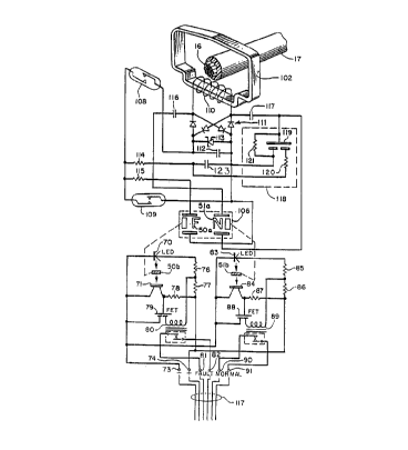
Referring to Figure 7, the necessary signals for
actuating the "F" and "N" optical displays are provided by a
line-powered circuit within housing 22. In particular, the
circuit includes a full-waive bridge rectifier 60 having one
25 input terminal connected to the capacitive coupling plate 25
and its othc=_r input terminal connected to ground through
ground lead 29. Thus connected the bridge rectifier network
is capaciti~~ely coupled to the monitored conductor 11 and
produces as a result of AC voltage on that conductor a
10
CA 02100651 1999-06-16
direct current at its output terminals. The output
terminals are connected to charge storage means in the form
of a capacj.tor 62 which develops a charge at a voltage level
dependent on a zener diode 61 connected across the
capacitor.
Capon occurrence of a fault current, capacitor 62
is momentarily connected by a fault current-actuated reed
switch 26 t.o additional charge storage means in the form of
a display capacitor 63 such that a portion of the charge on
capacitor 62 is transferred to capacitor 63. A series-
connected resistor 64 serves to reduce the rate at which the
charge is transferred to prevent damage to the switch
contacts from excessive current flow. The voltage developed
across disF~lay capacitor 63 as a result of the transferred
charge sArves as a voltage source, providing a voltage
signal which is applied to the "F" optical display
electrodes of component 27 through resister 65 such that the
transparent. indicator electrode 50a displays an "F" character
to the user- and optical shutter electrode 50b is closed.
This display continues until the charge on capacitor 63
depletes with time to a voltage level insufficient to
maintain the alignment of the molecules in the nematic
liquid cry~~tal lay=r. In practice, capacitor 63 will
have sufficient charge to maintain the "F" indicator and
optical shutter for up to 36 hours, this time being
primarily dependent on the net charge transferred to the
capacitor a.nd the internal leakage of the capacitor. A
11
CA 02100651 1999-06-16
lesser duration may be provided if desired by increasing the
current drain from the capacitor.
Fault indicator 20 may also include an "N" segment
display and optical shutter to indicate the presence of
5 operating voltage on monitored conductor 11. In particular,
this is accomplished by connecting the "N" display
electrodes which inr_lude backplane electrode 45 and
transparent indicator electrode 51a of display component 27
to the capacitive coupling plate 25 through a resistor 66
10 and coupling capacitor 67. In the presence of alternating
current on the monitored conductor the "N" display 34
appears and the user is informed that the conductor is
powered. At the same time, optical shutter electrode 51b is
closed, signaling voltage presence at a remote location in a
15 manner to be described.
It will b.=_ noted that the "F" display 33 and its
associated optical shutter electrodes are controlled by
direct current supplied by capacitor 63, whereas the "N"
display 34 a.nd its ~~ssociated optical shutter electrodes are
20 powered by alternating current derived through resistor 66
and capacitor 67. 'Thus, the two displays are independent of
each other.
FL.rthermore, it will be noted that the reflecting
panel 53 of component 27 is dimensioned to reflect only
25 light associated with the "F" and "N" display portions, and
not light associated with the optical shutter electrode
portions. P.s will :be described, this allows the optical
shutter electrode portions to control light passing through
the component.
30 Once the fault indication has occurred, should it
12
CA 02100651 1999-06-16
be desired to cancel the "F" indication, as for example when
re-powering the affected circuit after a transient fault, it
is only necessary to discharge capacitor 63 by actuating the
optionally provided manual reset reed switch 28 by
momentarily applying a magnetic field at the exterior of the
housing. To this end, the reed switch is preferably located
at an accessible lacation near the front face~plate of the
housing, with its axis aligned generally parallel to the
axis of conductor 1.1 so that the switch will not be actuated
by fault currents in the conductor.
In many applications it is desirable that
following a fault occurrence a fault indicator be self-
resetting, i.e., automatically return to a reset state upon
restoration of voltage to the monitored conductor. As shown
in Figure 7, this may be accomplished by providing an
optional reset circuit 68 which includes a field effect
transistor (FET) 69 having principal source and drain
electrodes connected through a resistor 56 to capacitor 63,
and a high impedance gate electrode coupled to the monitored
AC conductor through the "N" display optical shutter
electrode circuit.
Upon restoration of voltage in the conductor, FET
69 is caused to conduct and discharge capacitor 63. The
fixed series resist=ance reduces the rate discharge through
the principal electrodes of FET 69 to preclude capacitor 63
from being discharged during a fault, prior to interruption
of voltage on the monitored conductor, as well as preventing
the discharge current from exceeding the limits of the FET.
13
CA 02100651 1999-06-16
An additional resistor 57 connected between the drain and
gate electrodes biases the device to a cut-off state in the
absence of a signal on the date electrode.
In accordance with the invention, the occurrence
of a fault is signaled at a location remote from housing 22
by means of a signaling circuit including a light emitting
diode (LED) 70 within housing 22, which projects a light
beam through the optical shutter electrode portion 50b of
component 27. After passing through the optical shutter
electrode the beam is received by a Darlington
phototransi.stor 71, which provides an impedance change with
changes in the amplitude of incident light. The LCD optical
shutter electrode !50b, LED 70 and phototransistor 71 may be
arranged in a compact assembly 72 which provides electrical
isolation between the sensing circuits associated with the
LCD device and the monitored AC source, and the control
circuitry associated with the phototransistor 71.
Power is supplied to the signaling circuit through
contacts 73 and 74,which may be contained in housing 22 and
connected through .individual conductors in a multi-conductor
cable 75 to a remote DC source. LED 70 is powered from this
source through a pair of resistors 76 and 77, and
phototransistor 71 is connected to the source through a
resistor 78. A threshold level for actuation of the alarm
circuit is established by a field effect transistor 79,
which energizes a relay 80 from the DC source.
Llpon the occurrence of a fault current the light
14
CA 02100651 1999-06-16
incident on photo transistor 71 increases, causing the
impedance of the transistor to decrease, and the voltage
applied to the gate electrode of FET 79 to increase. This
causes the FET to conduct and actuate relay 80. The relay
contacts in turn provide a signal at terminals 81 and s2 for
actuation, through individual conductors in cable 75, of a
remote alarm or other switching function.
With actuation of relay 80 the voltage drop across
resistor 77 increa:~es, causing LED 70 to produce less light.
This in turn causes the impedance of photo transistor 71 to
increase and thus provide a latching function with helps to
maintain relay 80 energized.
Relay 80 continues to be energized until tha "F"
indication is reset, at which time the light incident on
photodetector 71 increases and the impedance of the
photodetector decreases to a level where FET 79 is no longer
conductive. At this time relay 80 is de-energized, the
relay contacts open and the control effect is no longer
present on termina:Ls 81 and 82.
The occurrence of an "N" display can be similarly
signaled to the remote location. In particular, a second
LED 83 is arranged to project a light beam through the "N"
optical shutter electrode to a phototransistor 84, which
together w~th resistors 85, 85 and 87 operates in the manner
of phototransistor 71 to control an FET 85 and relay 89 to
provide a control signal at contacts 90 and 91 associated
with cable 75.
CA 02100651 1999-06-16
The invention may also be utilized in a current-
powered application. Referring to Figures 8-11, a current-
actuated remote-indicating fault indicator 100 constructed
in accordance with the invention may include a generally
rectangular housing 101 secured to a monitored cable 17 by
means of a resilient magnetic pole assembly 102 which
encircles tine cable. The magnetic pole assembly is held in
a closed poaition by a spring 103 which secures cable 17
against a V-shaped recess in the housing.
Within housing 101 fault indicator 100 includes a
circuit board 104 (Figures 10 and 11) on which the principal
components of the indicator are mounted. A layer of potting
compound 10!i seals the circuit board within the housing.
Circuit status is indicated locally at the fault indicator
by a high impedance liquid crystal optical display and
optical shwtter electrode component 106, which is mounted on
the circuit board and may be identical in construction and
operation to the component 27 previously described.
Component 106 is positioned behind a viewing window 107 such
that the "F~' and "I;f" displays of the component can be
readily observed from the exterior of the housing. A first
reed switch 108 (Fi.gure 10) aligned generally tangentially
to the moni~ored conductor senses the occurrence of fault
currents in the conductor. An optional second reed switch
109 aligned generally parallel to the axis of the monitored
conductor a:Llows the user to reset a fault indication by
means of an external magnet.
16
CA 02100651 1999-06-16
Operating power for the circuitry of fault
indicator 7.00 is obtained by means of a winding 110 disposed
on magnetic; core 102 within housing 101. In the presence of
alternating current in the monitored conductor 16 a current
is induced in winding 110. As shown in Figure 12, the
induced alternating current is supplied to the input
terminals of a bridge rectifier network 111, wherein it is
rectified to develop a charge within a capacitor 112. A
zener diode 113 connected across this capacitor limits the
voltage developed across the capacitor.
Upon occurrence of a fault current in the
monitored conductor, reed switch 108 momentarily closes and
a portion of the charge developed in capacitor 112 is
conveyed through the switch to a second capacitor 123.
Capacitor 123 is connected to the "F" optical display
electrode and the associated optical shutter electrode of
component 1D6 such that the display electrode 50a is caused
to display the character "F" to the user and the optical
shutter electrode SOb of the component is rendered opaque to
signal that. a fault has occurred. A resistor 114 is
connected i.n series with capacitor 123 to limit current flow
through the: switch contacts, and a resistor 115 is connected
in series with the "F" display electrodes. In practice, the
"F" display may last 36 hours or more, depending primarily
on the charge transferred to capacitor 123 and the internal
leakage current of the capacitor. Capacitor 123 may be
discharged by the user at any time by actuation of the
17
CA 02100651 1999-06-16
optional reed switch 109 by means of an external magnet.
T:he "N" display of display component 106 may be
actuated by the current induced in winding 110 when the
monitored conductor 16 is powered. A pair of capacitors 116
and 117 connect the "N" display electrodes to winding 110 to
this end.
Tlaus, in the manner of the previously described
capacitivel;~-coupled fault indicator of Figures 1-7, upon
occurrence of a fault an "F" indication is provided which
indicates to the user that a fault has occurred. Thia
indication ~..~emains until the reset switch 109 has bean
actuated by the user, or until capacitor 123 discharges to a
voltage lev~sl below that sufficient to maintain the
indication on display component 106. An "N" indication
appears whenever the monitored conductor is energized.
At the same time, the corresponding optical
shutter ele~~trodes 50b and 51b, in conjunction with an LED
light source, and signaling circuitry including a
photodetector responsive to light transmission through the
optical shutter, signal the fault and powered states to a
remote location through a cable 117.
A.utomatir resetting of fault indicator 100 may be
achieved by means of an optional reset circuit 118 similar
to the previously described reset circuit 68. Zn
particular, the reset circuit may include an enhanced FET
119 having principal source and drain electrodes connected
to capacitor 123 through a current limiting resistor 120,
18
CA 02100651 1999-06-16
and the high impedance gate electrode may be coupled to
winding 110 'through the ~~N~~ display capacitor 117, or
through an a<iditional capacitor, and biased to cut-off by a
resistor 121. Upon restoration of current in conductor 16,
FET 119 is rendered conductive and capacitor 123 is
discharged to terminate the ~~F" indication.
While the use of other types of high impedance
voltage-actuated light controlling devices such as Kerr
cells, where~.n a dielectric under electrostatic stress
becomes doub7.y refracting so as to convert plane-polarized
light to elliptical polarization, is possibla, liquid
crystal disp7.ay (LCD) components, because of their extremely
high input impedance, are particularly well adapted to the
invention. The high input impedance of these devices,
typically in excess of 10x10-15 ohms, results in a very low
current drain from the display capacitor. This allows the
capacitor to retain sufficient charge for operating the
display over an extended period, typically in excess of 36
hours, limited primarily by the internal leakage current of
the capacitor.~. In practice, this is more than sufficient
time for a repair crew to locate and repair a fault, even in
a large distribution system.
Furthermore, depending on the particular liquid
crystal material usE:d, LCD components exhibit a well defined
threshold voltage over a wide range of ambient temperatures
below which the display does not respond to an applied
signal. In one successful embodiment of the invention using
19
a hype '7 twisted nematic field effect LCD manufactured by
Standish Tndustries, Inc. of Lake Mills, Wisconsin, U.S.~.,
this threshold is 2.0 volts, which is sufficiently high to
prevent the display from falsely responding to residual
voltages, but not so high as to require an undesirably large
charge on the display capacitor.
While the illustrated embodiments provide a visual
display as well a a remote signaling ouptut, it may be
desirable in some applications to omit the visual
indications and provide only the optical shutters and their
associated signaling circuitry for indications at a,remote
location.
While particular embodiments of the invention have
been shown and described, it will be obvious to those
skilled in the art that changes and modifications may be
made therein without departing from the invention in its
broader aspects, and, therefore, the aim in the appended
claims is to cover all such changes and modifications as
fall within the true spirit and scope of the invention.
20