Language selection

Search

Patent 2100727 Summary

Third-party information liability

Some of the information on this Web page has been provided by external sources. The Government of Canada is not responsible for the accuracy, reliability or currency of the information supplied by external sources. Users wishing to rely upon this information should consult directly with the source of the information. Content provided by external sources is not subject to official languages, privacy and accessibility requirements.

Claims and Abstract availability

Any discrepancies in the text and image of the Claims and Abstract are due to differing posting times. Text of the Claims and Abstract are posted:

  • At the time the application is open to public inspection;
  • At the time of issue of the patent (grant).
(12) Patent: (11) CA 2100727
(54) English Title: OPTIMIZATION CIRCUIT
(54) French Title: CIRCUIT D'OPTIMISATION
Status: Deemed expired
Bibliographic Data
(51) International Patent Classification (IPC):
  • H03K 17/00 (2006.01)
  • H03K 17/14 (2006.01)
  • H03K 19/003 (2006.01)
(72) Inventors :
  • ORCHARD-WEBB, JONATHAN (Canada)
(73) Owners :
  • MITEL CORPORATION (Not Available)
(71) Applicants :
(74) Agent: MARKS & CLERK
(74) Associate agent:
(45) Issued: 2001-06-12
(22) Filed Date: 1993-07-16
(41) Open to Public Inspection: 1995-01-17
Examination requested: 1998-07-23
Availability of licence: N/A
(25) Language of filing: English

Patent Cooperation Treaty (PCT): No

(30) Application Priority Data: None

Abstracts

English Abstract


A method of improving the performance of an active
semiconductor device with a voltage-controllable channel
length, comprises providing a matched reference component
having similar operating characteristics to the active
semiconductor device, continually monitoring the breakdown
voltage of the matched reference component, and maintaining
the operating voltage of the.active semiconductor device to
lie just below the measured breakdown voltage of the matched
reference component. In this way, the performance of the
active component can be optimized.


Claims

Note: Claims are shown in the official language in which they were submitted.


THE EMBODIMENTS OF THE INVENTION IN WHICH AN EXCLUSIVE
PROPERTY OR PRIVILEGE IS CLAIMED ARE DEFINED AS FOLLOWS:

1.A method of improving the performance of an active semiconductor device with
a
voltage-controllable channel length, comprising the steps of:
a) providing a matched reference component having similar operating
characteristics to said active semiconductor device;
b) continually supplying a current to said matched reference component to
cause
the breakdown thereof;
c) continually monitoring the breakdown voltage of said matched reference
component; and
d) continually maintaining the operating voltage of said active semiconductor
device just below said breakdown voltage.
2. A method as claimed in claim 1, wherein said matched reference component is
located in close physical proximity to said active semiconductor device so as
to be
influenced by the same external factors as the active semiconductor device.
3. A method as claimed in claim 1, wherein said breakdown voltage is presented
to
an operational amplifier as a reference voltage, and said operational
amplifier produces an
output voltage that sets an output voltage of the active semiconductor device
at a desired
level just below its breakdown voltage.
4. A method as claimed in claim 1, wherein said reference component is
designed to
breakdown at a voltage slightly lower than the active semiconductor device.
5. An optimization circuit comprising:
a) an active semiconductor device having a channel with an identifiable
breakdown voltage and a length determined by an applied operating voltage;
b) a matched reference component having similar operating characteristics to
said
active device;
c) means for continually supplying current to said matched reference component
to cause the breakdown thereof;
d) means for continually monitoring the breakdown voltage of said matched
reference component; and
-6-


e) means for adjusting said applied voltage to maintain the operating voltage
of
said device at a level just below said breakdown voltage.
6. An optimization circuit as claimed in claim 5, characterized in that said
matched
component is located in close physical proximity to said semiconductor device
so as to be
influenced by the same external factors as said active semiconductor device.
7. An optimization circuit as claimed in claim 6, wherein said means for
adjusting
said applied voltage comprises an operational amplifier having a first input
connected to
said matched reference component and a second input receiving a signal
proportional to
said applied voltage.
8. An optimization circuit as claimed in claim 7, wherein said second input of
said
operational amplifier is connected to a potential divider receiving said
applied reference
voltage.
9. An optimization circuit as claimed in claim 5, wherein said active
semiconductor
device is a CMOS device.
10. An optimization circuit as claimed in 5, wherein said matched reference
device is
designed to break down at a voltage slightly lower than said active
semiconductor device.


-7-

Description

Note: Descriptions are shown in the official language in which they were submitted.


CA 02100727 2000-07-18
This invention relates to an optimization circuit for
use with an active semi-conductor device, such as a MOS or
CMOS field effect transistor.
A wide range of gate lengths is observed in advanced
CMOS and GaAs devices. This gives rise to a wide range in
electrical parameters, particularly speed and breakdown
voltage. Similar problems occur in bipolar devices, where
base width is difficult to control.
As a result of the spread of breakdown voltages from
one device to the next, it is customary to design circuitry
to operate well away from the breakdown voltage so that the
circuit specifications do not result in a significant
wastage of components and reduction in product yield. The
unfortunate consequence of this requirement is that the
operating frequency of the circuit is reduced. The
reduction in operating frequency is compounded by the Early
effect, which causes the frequency response to decrease as
the supply voltage is moved further away from the breakdown
voltage.
Previously, guard banding has been employed to
distance the circuit operating conditions from the minimum
breakdown voltage but inevitably speed performance is
adversely affected. There is a trade-off between
performance and reject rate. The smaller the guard band,
the better the performance but the higher the reject rate.
In the production of any semi-conductor device, the
objective is to obtain the lowest reject rate, or highest
yield, possible. The object of the invention is to
alleviate the aforementioned problems.
1


CA 02100727 2000-07-18
In accordance with the present invention, there is
provided, a method of improving the performance of an
active semiconductor device with a voltage-controllable
channel length, comprising the steps of, providing a
matched reference component having similar operating
characteristics to said active semiconductor device,
continually supplying a current to said matched reference
component to cause the breakdown thereof, continually
monitoring the breakdown voltage of said matched reference
component and continually maintaining the operating voltage
of said active semiconductor device just below said
breakdown voltage.
The invention can be applied to any electrical circuit
which has well matched active components. In the case of
discrete components, the operating voltage can be set by a
linear voltage control circuit comprising an amplifier and
a power transistor forming a pass element. The function of
the pass element is to reduce the voltage to a value of Vo
below the reference device breakdown voltage. In the case
of a bipolar circuit, the same technique can be used or an
operational amplifier can be used to buffer the reference
voltage, with the required voltage drop being obtained from
a level shifting circuit.
The reference device is preferably maintained in close
physical proximity on the same circuit to the active
device. As a result, the reference component is influenced
by the same external factors as the active component and
consequently its breakdown voltage varies in a similar
fashion.
2


CA 02100727 2000-07-18
Preferably, a small current is forced through the
reference component with a current limiting device to cause
it to breakdown, and the breakdown voltage is then
presented to an input of an operational amplifier, which at
its output provides a control voltage.
In a further aspect, the invention provides an
optimization circuit comprising, an active semiconductor
device having a channel with an identifiable breakdown
voltage and a length determined by an applied operating
voltage, a matched reference component having similar
operating characteristics to said active device, means for
continually supplying current to said matched reference
component to cause the breakdown thereof, means for
continually monitoring the breakdown voltage of said
matched reference component, and means for adjusting said
applied voltage to maintain the operating voltage of said
device at a level just below said breakdown voltage.
The described circuit has the advantage that each
semiconductor device is operated as close as possible to
the optimum breakdown voltage without actually causing
breakdown. As a result, regardless of processing
variations, the circuit will always operate very close to
the maximum possible speed.
The invention will now be described in more detail,
way of example only, with reference to the accompanying
drawings, in which:-
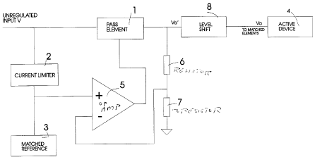
Figure 1 is a generalized block diagram of an
optimization circuit in accordance with the invention; and
3


CA 02100727 2000-07-18
Figure 2 is a circuit detail of a specific
implementation of an optimization circuit, in which the
reference device is designed to breakdown at a voltage
lower than the active circuit devices so as to eliminate
the need for a pass element.
Referring now to the Figure 1, an unregulated input
voltage V is applied to a pass element 1 and current
limiter 2. The current limiter 2 forces a small current
through matched reference component 3, causing it to break
down. The matched reference component 3 is chosen to have
operating characteristics as close as possible to an active
channel device 4, such as a CMOS FET. The matched
component 3 is also placed in close physical proximity to
the device 4 so as to be influenced by the same external
factors. The matched reference component therefore behaves
in the same manner as the active device 4.
The breakdown voltage db of the matched reference
component 3 is continually presented to a non-inverting
input of operational amplifier 5 having an inverting input
connected to the mid-point of a potential divider formed by
resistors 6, 7. The output of operational amplifier 5 is
connected to pass element 1.
The operational amplifier 5 is connected as a voltage
regulator in which the potential divider can be adjusted to
set the voltage Vo' to be close to the matched reference
voltage. Level shifter 8 then sets the voltage drop to a
value Vo, which is just below the breakdown voltage of the
frequency limiting circuitry.
4


CA 02100727 2000-07-18
Figure 2 shows a more detailed implementation of the
optimization circuit.
The reference circuit, generally designated 10,
comprising a reference MOS FET 11 connected in series with
a load 14, which may be a resistor or MOS transistor, for
supplying a small current to the reference MOS FET 11. The
reference MOS FET 11 has a channel length L = La - b- where
La is the critical channel length at which breakdown occurs
of the critical transistors in the active circuit, and b is
a small increment. For a MOS device, the small reduction -
in channel length ensures that the reference device breaks
down at a slightly lower voltage than the active circuit
devices. This arrangement eliminates the need for a pass
element or level shifting circuit, but the matching
characteristics still remain very good. Operational
amplifier 5 has transistors with a channel length L > La.
In operation, the active circuit has a first set of
non-critical transistors (not shown) that are operated with
channel lengths L such that L > La, and these transistors
are supplied by the external supply 13. A second set of
critical transistors (not shown) are operated with channel
lengths La, and these are supplied by the output of the
operational amplifier 5, which has one input connected to
the reference MOSFET 11.
The above circuit ensures that regardless of
processing variations, the circuitry will always operate
very close to the maximum speed possible.

Representative Drawing
A single figure which represents the drawing illustrating the invention.
Administrative Status

For a clearer understanding of the status of the application/patent presented on this page, the site Disclaimer , as well as the definitions for Patent , Administrative Status , Maintenance Fee  and Payment History  should be consulted.

Administrative Status

Title Date
Forecasted Issue Date 2001-06-12
(22) Filed 1993-07-16
(41) Open to Public Inspection 1995-01-17
Examination Requested 1998-07-23
(45) Issued 2001-06-12
Deemed Expired 2003-07-16

Abandonment History

There is no abandonment history.

Payment History

Fee Type Anniversary Year Due Date Amount Paid Paid Date
Application Fee $0.00 1993-07-16
Maintenance Fee - Application - New Act 2 1995-07-17 $100.00 1995-07-17
Registration of a document - section 124 $0.00 1996-01-18
Maintenance Fee - Application - New Act 3 1996-07-16 $100.00 1996-06-06
Maintenance Fee - Application - New Act 4 1997-07-16 $100.00 1997-07-11
Registration of a document - section 124 $50.00 1998-02-16
Maintenance Fee - Application - New Act 5 1998-07-16 $150.00 1998-07-10
Request for Examination $400.00 1998-07-23
Maintenance Fee - Application - New Act 6 1999-07-16 $150.00 1999-06-03
Maintenance Fee - Application - New Act 7 2000-07-17 $150.00 2000-05-18
Final Fee $300.00 2001-03-09
Maintenance Fee - Application - New Act 8 2001-07-16 $150.00 2001-04-20
Registration of a document - section 124 $50.00 2001-05-04
Owners on Record

Note: Records showing the ownership history in alphabetical order.

Current Owners on Record
MITEL CORPORATION
Past Owners on Record
ORCHARD-WEBB, JONATHAN
Past Owners that do not appear in the "Owners on Record" listing will appear in other documentation within the application.
Documents

To view selected files, please enter reCAPTCHA code :


To view images, click a link in the Document Description column. To download the documents, select one or more checkboxes in the first column and then click the "Download Selected in PDF format (Zip Archive)" or the "Download Selected as Single PDF" button.

List of published and non-published patent-specific documents on the CPD .

If you have any difficulty accessing content, you can call the Client Service Centre at 1-866-997-1936 or send them an e-mail at CIPO Client Service Centre.


Document
Description 
Date
(yyyy-mm-dd) 
Number of pages   Size of Image (KB) 
Cover Page 2001-05-29 1 27
Abstract 1995-08-26 1 36
Claims 1995-08-26 2 104
Drawings 1995-08-26 2 48
Description 1995-08-26 5 258
Cover Page 1995-08-26 1 33
Claims 2000-07-18 2 75
Drawings 2000-07-18 2 22
Description 2000-07-18 5 206
Representative Drawing 2001-05-29 1 6
Representative Drawing 1998-07-28 1 7
Assignment 1993-07-16 23 1,051
Assignment 2001-06-13 2 99
Prosecution-Amendment 2000-05-04 2 67
Prosecution-Amendment 2000-07-18 11 375
Correspondence 2001-03-09 1 37
Assignment 2001-05-04 13 780
Prosecution-Amendment 1998-07-23 1 39
Fees 1996-06-06 1 63
Fees 1995-07-17 1 33