Note: Descriptions are shown in the official language in which they were submitted.
2 1 0 1 1 28
- 1 -
SINGLE MIRROR LIGHT-EMITTING DIODES
WITH ENHANCED INTENSITY
Technical Field
This invention concerns light-emitting diodes (LEDs) with optimized intensity
of emission.
Background of the Invention
Light Emitting Diodes (LEDs) are preferred over lasers for short distance fiber
communications because of their greater reliability and lower cost, although the optical
power coupled into a fiber is smaller. Since their emission is purely spontaneous,
LEDs are less susceptible to power changes with temperature. Therefore, it is ofinterest to seek improvements in output intensity without resorting to a structure with
optical gain.
By positioning an optical reflector behind a thick spontaneously emitting
surface, the far field intensity of an LED could be doubled, compared to an LED
without a mirror. For example, see T. Kato et al. "GaAs/GaAlAs Surface Emitting IR
LED With Bragg Reflector Grown MOCVD", Journal Crystal Growth. 107, 1991, pp.
832-835. The normal incidence emission can also be enhanced by making the activeregion thin, and placing it in the anti-node of an optical mode. Deppe et al.
demonstrated with a single quantum-well structure that the enhancement and inhibition
of emission depends on the quantum well placement relative to a single reflective
mirror. See D. G. Deppe et al., "Optically-Coupled Mirror Quantum Well InGaAs-
GaAs Light-Emitting Diode", Electronic Letters, Vol. 27, 1990, pp.1165-1166. Also
see U.S. Patent 5,089,860 issued February 18, 1992, to Dennis G. Deppe et al. While
Deppe et al., discussed the dependency of the normal incidence of emission on the
position of the single quantum well structure relative to the single mirror, no
quantitative consideration was given to the emission intensity of such single-mirror
devices. Applicants have discovered that while the normal incidence of emission of a
device with a single quantum well was enhanced due to the positioning of the quantum
well in the anti-node of the optical mode of the LED, increase in an operating current
beyond a certain limit led to the saturation of the emission intensity of such an LED.
2 1 0 1 1 28
- la-
Summary of the Invention
In accordance with one aspect of the invention, there is provided a light-
emitting diode (LED) which comprises a semiconductor structure including an active
5 region, and a top electrode and a bottom electrode to the structure, wherein said active
region comprises a plurality of quantum wells positioned relative to the top electrode
so as to fit into an anti-node of an optical mode of the LED.
In accordance with a further aspect of the invention, there is provided a light-emitting diode (LED) which comprises a semiconductor structure comprising Groups10 III-V semiconductors and a top and a bottom electrode to the structure, said structure
comprising in an ascending order from the bottom electrode a substrate, a bottomconfining region, an active region, a top confining region, and a contact layer, a
dielectric barrier layer on top of the contact layer has a window exposing a small area
of the contact layer, said top electrode being in contact with said dielectric barrier layer
15 and, through said window, with the contact layer, wherein said active region comprises
a plurality of quantum wells positioned relative to the top electrode to fit into an anti-
node of an optical mode of the LED.
In particular, this invention embodies single mirror light-emitting diodes (LEDs)
with enhanced intensity. The LEDs are Group III-V and/or II-IV compound
20 semiconductor structures with a single metallic mirror. The enhanced intensity is
obtained by placing an active region of the LED having from two to ten, preferably
" A'
21 01 1 28
from f to eight, qu~lulll wells at an anti-node of the optical mode of the device
created by a ncarby metallic mirr~r. Such muldqudlllulll well LED structures exhibit
enhqnre~l efflrienries ap~.uacking that of a perfect isotropic emitter.
Brief Description of the Drawin~
S FIG. 1 is a sshem^fic l~pl~sc,lt~tion of a ~ Clul~ for a multiple
qusntllm well LED with a m~tqllir mirror,
FIG. 2 is a plot of a normal inridçnr,e optical mode for the device shown
in FIG. l;
FIG. 3 is a plot of conduc~r and valence bands for the device shown in
10 FIG. l;
FIG. 4 is a plot of 295K spectra through the top of a single 4uan~u~
well device with a ~n~ nsparent silver top mirror, showing the effects of band
filling;
FIG. S is a plot of spectra through the top of a se.llilldllsparent silver
15 mirror for 1, 4, 6 and 8 4uar lull~ well sq-mrles for 2, 8, 12 and 16 mA pump currents,
re~p~;li./ely; and
FIG. 6 is a plot l~ l ,se ~ ~t;ng the int~ nsily of emicsi~ n in a narrow solid
angle versus pump current for 1, 4, 6 and 8 4uA~.n...~-well samples and the line(dashed) l~,~n se-r.t;--g a perfect effiçienry LED without mirror and with an
20 isotropically emifflng active region.
Detailed Description
In FIGs. 1, 2 and 3 are shown, l~ ly, the schçm~tir ~ c for a
multi-quantum well LED, the optical mode of the device, and the schf~ ;s
~ At;on of condu( tion and valence bands of the device. Also shown, in
25 ph~ntom~ in FIG. 1 is a sçhe.n~ic position of a single quantum well and in FIG. 3 a
schemqtic position of cond~lction and valence bands for the single quantum well.For illustration l~ul~oses, various (1im~ncions of the drawings are drawn not tO scale.
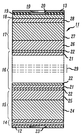
In FIG. 1 is shown a schçmqtil~ rc~lcse~lAlion of an LED, d~signqted
generally as 10, embodying the invention. LED 10 in~ludçs a sçmirQntluctor
30 stlu~-lul~ decigrq-~A generally as 11, and a bottom elc~ odL, 12, and a top electrode,
13, to the structure. The semiconductor materials of the sçmicond~lctor structure are
Group m-v or II-IV selllico~-d~lc~ors such as GaAs, AlGaAs, GaInAs, AlGaInAs,
InP, Ga~P, GaInPAs and other group m-v and II-VI compound semiconductors
lattice mAtcl~ to GaAs and/or to InP. Structure 11 includes~ in an accen-ling order
35 from bottom electrode 12, a substrate, 14, a bottom confining region, 15, an active
region, 16, a top confining region, 17, and a contact layer, 18. An inculAting layer,
210~23
19, with a window, 20, is bel~.~n the contact layer and top electrode 13.
A more det~ile-l construction of LED 10 is as follows:
Substrate 14 is a heavily doped m-v or II-VI semiconductor. Typically,
the thirlrness of the substrate ranges from 50 to 650 llm, and the doping
concentration ranges from 1 x 10¹⁷ to 4x 10l8 cm-3.
~ onfining regions 15 and 17 are provided to confine active region 16.The thichlesses of these regions range from 0 to 2 ~lm.
Active region 16 is a multiquantum well (MQW) structure including
from two to 10 quantum wells. Each quantum well includes a narrow-gap
10 semi~on-luctor 21 from 1 to 30 nm thick clad by wide-gap semirQn-luctors, 22, from
1 to 20 nm thick each.
Contact layer 18 is a highly doped layer from 0.01 to 0.1 ~m thick and
with doping conce.,l.ation ranging from 1 x 10¹⁹ to 1 x 102 cm~3, preferably about
5x10l9 cm~3. The contact layer is provided to f~ril jt~te establishrn~nt of a non-
alloyed ohmic contact between top electrode 13 and the se~lliconductor structure.
A thin layer 19 of dielectric material, such as SiO 2, Si 3 N4, borosilicateglass such as Vicor~, etc. is formed on top of contact layer 18 in a thickness of from
0.01 to 0.1 ~lm. Layer 19, which acts as a barrier between contact layer 18 and top
electrode 12, has a centrally located window 20 perrni~ting direct contact between
20 top electrode 13 and contact layer 18.
Top electrode 13 is selected from metals which are electrically
conducting, have low resistivity and are highly reflective, with reflectivity ranging
bel~. ~n 90 percent and 99 percent and higher. Metals may be selected from Ag, Au,
AuBe, AuZn, Cr, and Ti. Provision of window 20 in layer 19 enables passage of
25 opela~ulg current from top electrode 13 to bottom electrode 12 through a narrow
p~ ~9ge defined by the window. The top electrode is from 30 to 5,000 nm thick.
Bottom electrode 12, ranging from 0.1 to 10 llm in thickness is formed
on the bottom surface of substrate 14 to provide for current flow through the active
region. The bottom electrode is of a metal which forms an ohmic cont~ct substrate
of the s~mi- onductor structure. Gold, indium and their alloys, such as AuGe, AuSn
and InSn, are suitable metals for the bottom electrode. A window, 23, is provided in
the bottom electrode to permit passage of spontaneous emi~sion from the active
region.
Layers of the semiconductor structure are grown upon substrate 14 by
such known methods as metal organic vapor phase epitaxy (MOVPE) or molecular
beam epitaxy (MBE) or hydride vapor phase epitaxy (VPE) which are well known.
21~128
- 4 -
Top metal electrode may be d~,posit~d by e~a~,alion at tc~ ~.alun,s of
ico~ .ctor structure ranging from 20 to 150C, or by s~)u~ g, or by electron-
beam deposition.
Active region 16 is positirJn~ relative to the optical mode of the device
5 so that each of the quantum wells of the active region is positioneA in an optical
anti-node of the device. The optical anti-node may be any one of anti-nodes relative
to the top electrode. Preferably, the anti-node second from the top is used for this
purpose. The number of quantum wells in the active region is selecte(l to provide an
op~ ulll output intensity from the device.
In the exemplary embodiment, the LED is an Al ,~ Ga ~ As / Ga As /
In y Ga 1 _y As structure, with x ranging from 0.1 to 0.4, and y ranging from O.OS to
0.25. In the pleftll.,d emb~in~nt~ the LED comprises, in an ~cen<ling s~quence,
0.1 to 2 ~lm thick AuGe electrode 12; 500 llm thick (001) ~riented n+ - doped (2 x
10l8 cm-3 ) GaAs substrate 14; bottom co~ ni~-g region 15 inr!llding an n-doped
(3x10l7 cm-3) Al0.2GaO.8As layer, 24, and a 40 nm thick undoped (intrinsic)
Al0.2GaO.8 As layer, 25; and active region 16 including a plurality of 5.6 nm thick
nn~lope 1 GaAs cl~l.1ing layers, 22, and a plurality of 10 nm thick undoped
InO.l6GaO.84As active layers 21 with each active layer being clad by two cladding
layers. The LED structure further includes top confining region 17 inclu-ling a 40
nm thick undoped Al0.2GaO.8 As layer, 26, a p-type doped ( 3x 10l7 cm-3)
Alo 2 GaO 8 As layer, 27, and a lS nm thick p+ - type doped (1 x 10l9 cm-3) GaAslayer, 28; lS nm thick p + - type doped (1 x 10 l9 cm - 3) GaAs contact layer 18; 120
nm thick SiO2 layer 19, with 10 ~lm fli~meter window 20; and silver top electrode
13. Depen-ling on the number of ~luanlum wells in the active region, the thi/~l~ness of
confining region layers 24 and and 27 will vary, l.,;,~;~ively, from 153 nm and 101
nm for a single quantum well, to 83 and 31 for ten quantum wells. Altern~ively,
layers 25 andlor 26 and 28 may be varied in ~hicl~ness in conjunction with the
variation in thic~ness of layers 24 and/or 27. The thir~n~ss variation is needed to
place the quantum wells into an anti-node of the optical mode of the LED.
In order to determine the power, efficiency, and spectral characteristics
of multi-quantum well LEDs, applicants have fabrira~l devices with from two to
ten multi-quantum wells. These structures were grown by molecular beam epitaxy
with 10 nm thick In 0.16 GaO.84 As wells, 21, and 5.6 nm thick GaAs barrier or
cl~l~ling layers, 22. For comparison, LEDs with a single quantum well centered in
35 the anti-node of the optical mode of the LED were f~bricate l in the same manner as
the multi-quantum well LEDs. A single quantum well, 29, and its band diagram
2 1 ~ 8
l~,p.csç~ ;on are shown in ph~ntom in FIGs. 1 and 3. In the LED with multi-
quantum wells, the col~rliflng regions, and especially top confining region 17, are
made thinner as the number of wells increases in order to position the active region
at the optical anti-node. As more wells are added, they cannot all be position~dS exactly at the anti-node, re~lucing the theoretical inlensily enh~n~e-..f,llt achievable
with the single mirror ~illUClUl~. The size of the anti-node is equal to ~ /2 where A is
the wavelength of light in the emittin~ (active) region, and the position, P, of the
center of the anti-node may be calculated as follows:
P = (2m~ R ) 4~
10 wherein m is an integer, and ~R is the phase change on reflection from the metal
mirror, and OC~R c 27~. Therefore, the center of each anti-node relative to the metal
mirror may be found at every ~/2. For example, ~ R for silver is ~ 4Ø In this
specific example, for an LED with GaAs substrate, Al 0.2 GaO.8 As confining regions,
In 0. 16 Gao.04 As wells, GaAs cl~d-iing layers, and silver mirror-electrode, the second
15 anti-node shall have the length (size) of 138 nm and the center of the second anti-
node shall be located 182 nm below the mirror.
For a device with one quantum well, the theoretical in~llsily
enh~nrement is about 3.8. For four, six, and eight quantum wells, the theoretical
intensity enh~nce.. nl~ are 3.4, 2.8, and 2.2, l~,s~clively. For the eight well20 structure, the active region is ap~r~ching a thil~kn~ss of A/2 whereby the m~enh~n~ement is 2Ø The enh~nce~ ll for greater thicl~nesses than this is just under
or over 2, depending on positioning.
The enh~ncen~nt process can be explained by constructive in~lÇel~,1ce
of the direct and rçflçct~ heams in the normal direction, giving for the maximum25 enh~n~e.m~nt a formula of ( 1+~)2, wherein R is the reflçct~nce of the mirror. For
a len~ e R=0.96, ignoring substrate-to-air reflections, the anti-node placelllent of
the single qu~ntum well enh~nces the normal ernissiQn intensity through the
substrate by a factor of 3.85. Rec~ e the metal mirror is in close p~ ,ity to the
4uantulll well, the anti-node position would change slowly with wavelength,
30 ensuring that the enh~nrement is mostly preserved over the entire spectlal range of
the LED.
The Ill~inlulll usable current at which an LED can operate is
detc.lllined by a n ulnber of factors including the effects of band filling. In FIG. 4 is
shown the emission spectra from the top of a device of a general construction shown
35 in FIG. 1, but with only one quantum well 29 and with a thin, 30 nm thick,
~10 il~8
sell~ nsparent top silver mirror, which simull~neously acts as the top electrode of
the device. The current is injected from a silver electrode with a ten ll~l0ll3etel
di~n~ter contact to contact layer 18. The silver electrode simllltptleously acts as a
mirror with a 96 percent reflection charncteriQtic~ In order to be able to measure the
S S~CLIuul and the degree of band filling at various voltage and power applicationc,
this emission takes place through the top electrode of the device, rather than through
the substrate. Such analysis would not be possible if emiccion would take place
through the bottom, becauc-~ of absorption of light by the substrate.
The amplitudes of the normal il~ci~lel-~G optical mode with the active
10 quantum well in the anti-node are shown in FIG. 4. The çmicsion is narrow at an
injection current of 0.6 mA, but begins to broaden by 2 mA, and is very broad by 6
mA. This inflic~tGs very high carrier conrçntrations~ and the broad spectra would
result in a large amount of ch~umalic dispersion in an optical fiber. Clearly, a single
4u~ltulll well cannot be ~ ~d very hard, and, ~ efol~, cannot achieve high
15 spont~ne~us output in~ncities For a rePcon~ble carrier lifetime of 1 ns, a 1 mA
pump current into a single well at a current density of 1.3 kA/cm-2 would result in a
carrier density of 8x 10l2cm~2 or about 8x 10l8 cm~3. At such injection ~;ull~nls, it
is expected for band filling to occur. The band filling ~csoci~tçd with high carrier
dencities results in higher chromatic dispersion in optical fibers, limiting
20 co~ ln~ tiQn bandwidth and distance.
In FIG. S is shown the top emics;con spectra through the 30 nm thick 10
~m in ~ m~ter silver mirror for four, six and eight quantum wells at an injection
current of 2.0 mA per well. Also shown, for co...p~ ;c-on, is the emission spectra for
one quantum well at the same injection current. This should result in similar carrier
25 d~ l,c; l ;r S in the wells and ~ ,~fol., similar spectra It is clear from the curves, and by
CCiulp~iSOII with FIG. 4 that the calrier ~iencities must indeed be similar. This shows
that placing mo~ wells within the anti-node of the optical mode is advantageous to
achieving high output powers.
The light output from the substrate of the LED versus current was
30 measured for the devices with four, six and eight quantum wells and, for
coml)~ison, with one quantum well. The results of these measul~l~eri~ are shown
in FIG. 6 at normal in-~idence. The light versus current curves for the multiplequantum well samples exhibit less current saturation than for the single quantumwell sample and achieve intensity levels that are useful for co.-~ ic~tions. The35 spectrally integrated intensity was measured with a calibrated small area detector
placed 7.5 cm away from the devices. Subsequently the intensity per steradian was
~101128
c~lrl-lq~ While the int~nsily drops with angle from the n~ rrnql, the normal
inrid~nc~ value is the most h~ t since, even when using lenses for coupling
LEDs and fi-hers~ only a small solid angle of the LED emi~sion is coupled into afiber. How much light is coupled into a fiber depends on the geomPt y of the
5 coupling optics, and the thir~ness of the substrate. The straight dashed line
coll~,s~ ds to the calculated light inDe"~ for a 100 percent internal quantum
efficiency isotropic emitter with an ideal R=0 antireflection co-q~ting This efficiency
cannot be achieved in con~en~ional LEDs with a non-unity intPrnal quantum
efficiency. However, devices embodying this invention approach this efficienry~
10 even without the use of antireflection co~tings- Initially, efficipncies are similar to
that of a perfect isotropic emitter, or 8.7 ~Wtsteradian/mA in air at normal incidence
from a mqteriql with refractive index n=3.5 at a wavelength ~0 = 0.93 ~Lm. This
efficiency is given by [(1240/ ~0) (1/(4 ~n2)]. Con~ ering the theoretical
enhqnremPnt factors of up to 4, it is possible for future devices to ~lrO ~l even
15 better. The optical coupling with the mirror is not e~;~d to signific~ntly affect
device speed, since the Einstein spo~t~nro~s emi~si~ n factor Asp will be increased
by less than five percent, only. An initial kink in the curves is caused by a small
leakage current of 300 ~A to 600 ~A.
As is schem~tir~lly ~ ,SenlCd in FIG. 6, intensities of emission
20 approaching that of a perfect isotropic emitter can be obtained in a multi-quantum
well, single-milTor LED by placing as many multi-quantum wells of the active
region in the anti-node of the optical mode as possible. The highest efficiency was
observed from a 6 quantum well s~mple, which has a theoretical enh~ncemen~ of 2.8
at this wavelength. Larger ~ meter devices would give similar efficiencies, with25 higher final power at plOpOl ~ionally higher current.
The one quanlulll well sample has a lower initial effici~ncy than the
other sn nrles, probably bec~-.ce of reduced capture of the ca~iers in the quantum
well. It is clear, ho~.e~er, that its light output saturates at a low pump current. This
saturation is caused partly by the combination of band filling and the effect of the
30 GaAs substrate absorption of light with wavelength shorter than 890 nm. With this
degree of band-filling, howe~,r, it is clear that one cannot pump the single qual1~u
well at high currents.
Additional advantages and m~lifiration~ will readily occur to those
skilled in the art. Therefore, the invention in its broader aspects is not limited to the
35 specific details, leplesent~live devices, and illustrated examples shown and
described. Accordingly, various m~ific~tions may be made without departing from
2101 1~8
- 8 -
the spirit or scope of the general in~ h~e concept as defined by the appended claims
and ~eir equivalents.