Note: Descriptions are shown in the official language in which they were submitted.
2101 140
HIGH DENSITY ELECTRONICS PACKAGE
HAVING STACKED CIRCUIT BOARDS
BACKGROUND
The present invention relates to electronic c~ one.lls having mllltiple circuit
board, and more par~cularly, to a high density electronics p~~ e having a plurality of
stacked circuit boards that are heat-sinlced to the houcin~
A co~on method of ...ounl;.~g ~li,~.hical circuit boards in elecl,onic housings
S is by using screws and standoffs. This method of ,llounling circuit boards l~Uil~,S
areas on the circuit boards to be kept clear of co,~l~onenls and .,-iu.;uill~, thus r~xluçing
the usable area of the boards. Multiple stacks of circuit boards using standoffs require
close tolçrance of screw holes, spacers, and circuit card/ heat sink ll"-'L ..e~s If this
is not the case, the ending tolerance stack-up prevents a proper fit and ~ligr m~nt within
10 the hollcing Current cylin-lnç~l housings and circuit boards are generally .~-o~n
- together using convention~l screw f~cteners and standoffs. This method makes the
electronics p~cL ~ge Aiffi~--lt to ~cs~ ..ble, provides poor vibration ~ ce and makes
thermal management ~iffin.llt
When a thermal path to an elc~ 0nic housing is needed, it often l.~quil~s the
15 design and installation of elaborate devices to accoml)lish this. The d.~l,&cL~ of such
thermal path ha,d~ are a minim~l thermal path and relatively weak ~lluclulal integri-
ty. To obtain structural stiffness, a large quantity of screws and st~nAoffc or ~iLre~
are l~UU~d, since SUppOIt is generally fil~iche~l only in small areas where t~h~e A;s~ t~
of the st~n-lQffs contact the circuit boards. The use of lightweight "touch" type connec-
20 tors (woe strips, fuzz buttons, etc.) are Aiffic -h to employ in this type of design due to
2101 140
the inherent lack of positioning capability. Distortion of circuit boards by use of screw
facteners may cause gaps bel~cen the cOIl~C~, thus creating board rnalfunctions.Therefore, it is an objective of the present invention to provide for a high
density elecll(,nics unit having a plurality of stacked circuit boards that is structurally
5 strong and has snffi~ent heat sinking
SUMMARY OF THE INVENTION
In order to meet the above objectives, the present invention is a high-density
elec~ ics package that houses a plurality of circular circuit boards, or cards, along
10 with heat sinks and circuit ir~t~,l.;onne~-lions in a single enclosure. The el~llunics pack-
age co., .1.. ;~es a housing having a conical shape disposed around at least a major
po~ion of the ~ ,hel ~ of an internal wall thereof. A first heat sink is dispos~ in the
housing that has a conical shaped ~li~hel~ that s]idably mates with the housing conical
shape along their ,~ e surfaces. First and second circuit boards, or cards, are
15 disposed on û~posed s~lrf~ces of the first heat sink and are ihllGl~onne~t~ by means of
a first set of mating conne~ul~ (licpose~l through the first heat sink. A second heat sink
is disposed in the housing that has a conical shaped periphery that is ~licrlt~d in a
direction oppo~i~ to the conical shape of the first heat sink
Third and fourth circuit boards, or cards, are disposed on oppos~d s~lrf~es of
20 the second heat sink and are in~onl-~tecl by means of a second set of mating connec-
tors di~osed through the second heat sink. A third set of mating conl-~lo, ~ h~tel~n-
nect the second and third circuit boards. An e~n~ble conical shaped ring is provid-
ed that tr~n~l~tes the conical shaped ~ ;l~h~ of the second heat sink to the vertical
inner wall of the housing. A fourth set of mating conl-ecl~ in~ ;onnP~t the fourth
25 ci-rcuit board and the elP~!. ;c~l int~- r~ board. A second eyp~n~ conical shaped
ring is provided to secure all boards and heat sinks within the housing. A small wedge
shaped block is used to spread the second conical shaped ring and induce a CO~I~,S
sion load on all internal assemblies.
The high-density electronics p~e~ may be used in ~.vs~ace qrp~ ^ ions
30 where ele~ unic circuit cards must be p~qr~q.~d as a lightweight, highly th~nqlly
conductive, and ~ clul~lly sound unit. The present invention is a unique p~q,~ ging
alIangement for circular circuit cards, for ~Y~q~rle, that maximizes the~ r~r
from the circuit cards to the housing. The present invention also provides e~ ,~e
rigidity, allowing the assembly to pass rigid military mi~cion l~uile,ll~,rl~. This is
35 achieved by bonding the circuit cards to the heat sinks that are pO~;I;Qn~l by the use of
conical angles on the heat sinks and by the use of the conical çYpqn~i~n ring that
provides both loc~lion~l and locking ~ n;C.~IC
- 2101 140
The electronics pq,rl~qge provides an -qscembly for ele~ lloilic circuit boards that
achieves suitable thermal management without the use of mi~cçllqn~olls -q-drlitiorql
hardware. The electronics pqr~qge provides for superior thermal transfer capabilities,
reduced circuit board flexing (especially advqntq~ous with HDMI technology), and5 less weight than previous pa~l~q~es, including card locks. ~cse-mbly is ar~Qmrlich~
by using a sek~l~ conical angle on the first heat sink that mates with a ~ hing coni-
cal angle on the hollsing The second heat sink also has a conical angle (that is located
in the opposile di~ ion of the first heat sink) that mates with an identir-q-l angle on an
e~p~qnsion ring used for positioning p~oses. This mounting feature provides auto-
10 matic heat sink to heat sink axial alignment regardless of tolerances, the.~ful~ simplify-
ing qcsembly and providing intim~te contact ~l~.~n the heat sinks and the housing,
and thus creating a thermal path from the circuit boards to the housing.
An embolim~nt of a el~llunics pa~q~e of the present invention has been
~lçcignecl, built and tested~ and SAI;5~GS the need for a lightweight, th~mqlly conduc-
15 tive, and structurally sound electronics p~r~age~ The present invention provides forgreater serviceability, easier f~bnc~ion, faster assembly, lower cost and in.,l~
design l~titude~ The present electronics p~clfage may be used in the aelos~ace industry,
although any applir~ti~ n requiring the use of a plurality of stacked circuit boards
operating in a hostile en~ "~nl would benefit from using the present invention. The
20 high-density electronics p~ ge also provides for s~nda~ ;on and m ldul--ity in
space vehicle and missile decigr c, for examplc.
The high-density el~LIonics p~r~age provides for a s~ r design for appli-
cations le4uiling an easily ~csçmh'e ~ ele~1l0iucs par~a~c The use of wedge-shaped
devioes for locating and lorl~ing, instead of Ihie~ed f~c~ n~ ~s, g~eatly e-nhqn~s the
25 se~vioe~bility, the~nal m~n~gem~nt and strength of el~;llolucs pa~a~s in which they
are employed. The ele,~ ics p~ ~ is easily f~l..; ab~ and l~l~S no special
tooling Assembly of c~....l~n~ into the honcillg is Pru~mrlished within minutes and
~lic~csembly is equally fast and easy.
- 2 1 0 1 1 4 0
3a
Aspects of the present invention are as follows:
An electronics package comprising:
a housing having a first conical shaped surface disposed around the
periphery of an int~.rn~l wall thereof;
S a first heat sink disposed within the housing that has a conical shaped
surface that slidably engages the first conical shaped surface along their
respective conical shaped surf~res;
first and second circuit boards disposed on opposite surfaces of the first
heat sink that are interconnected by first connection means disposed through thefirst heat sink;
a second heat sink disposed within the housing that has a conical shaped
surface that is oriented in a direction opposite to the conical shaped surface of
the first heat sink;
third and fourth circuit boards disposed on opposite surfaces of the
second heat sink that are interconnected by means of a second connection means
disposed through the second heat sink, and wherein the third circuit board is
also interconnected to the second circuit board by the first connection means;
an exp~n~l~hle conical shaped member that contacts the conical shaped
surface of the second heat sink along at least a portion thereof;
an electrical interconnection circuit board electrically connected to the
fourth circuit board that comprises means for coupling electrical signals to therespective circuit boards from outside the electronics package; and
a locking mech~ni~m that engages the housing and the electrical
interconnection circuit board, and forces the electrical interconnection circuitboard and exr~n~l le conical shaped member toward the first conical surface of
the housing, thus forcing the circuit boards and heat sinks against the first
conical surface on the inner wall of the housing, and thus securing the heat
sinks, circuit boards, and electrical interconnection circuit board in the housing.
An electronics package comprising:
a housing having an inner wall, a portion of which is a conical surface
disposed around the periphery of the intern~l wall of the housing;
2101 140
3b
a first heat sink disposed within the housing that has a conical shaped
surface that slidably engages the conical surface of the housing along their
respective conical shaped surfaces;
first and second circuit boards disposed on opposite surfaces of the firs
S heat sink that are interconnected by means of a first set of mating connectors
disposed through the first heat sink, and wherein the second circuit board has asecond set of connectors;
a second heat sink disposed within the housing that has a conical shaped
surface that is oriented in a direction opposite to the conical shaped surface of
the first heat sink;
third and fourth circuit boards disposed on opposite surfaces of the
second heat sink that are interconnected by means of a third set of mating
connectors disposed through the second heat sink and wherein the fourth circuit
board has a fourth set of connectors;
and wherein the second set of mating connectors of the second circuit
board interconnect to the third set of mating connectors of the third circuit
board;
an exp~n~l~hle conical shaped member slidably eng~ing the conical
shaped surface of the second heat sink and the inner wall of the housing;
an electrical interconnection circuit board electric311y connected to the
fourth circuit board by means of the fourth set of connectors that comprises
means for coupling electrical signals to and from the respective circuit boards
and circuitry disposed outside the electronics package; and
a locking mech~ni~m including a lock ring eng~ging the housing and the
electrical interconnection circuit board, and forcing the electrical interconnection
circuit board and exr~nd~hle conical shaped member toward the conical shaped
surface of the housing, thus forcing the heat sinks and circuit cards together to
secure them between the conical shaped surface of the housing and the locking
mech~ni.sm.
~.'
-3c- 21 0 1 1 40
An electronics package comprising:
a housing having an int~rn~l wall, a portion of which is a conical surface
that forms part of the int~rn~l wall of the housing;
a first heat sink having a conical shaped surface that slidably engages the
S conical feature of the housing along their respective wedge shaped surfaces;
first and second circuit boards disposed on opposite surfaces of the first
heat sink, and wherein the first circuit board has a connector that mates with
connector pins on the second circuit board, and wherein the connector and
connector pins are interconnected through an opening through the first heat sink;
a second heat sink that has a conical shaped surface that is oriented in a
direction opposite to the conical shaped surface of the first heat sink;
third and fourth circuit boards disposed on opposite surfaces of the
second heat sink, and wherein the third circuit board has a connector that mateswith connector pins on the fourth circuit board and wherein the connector and
the connector pins are inte~olmected through an opening through the second
heat sink, and wherein the third circuit board is connectf~i to the second circuit
board by a connectors on the second circuit board;
an expandable circular shaped ring that has a conical shaped surface that
is oriented in a direction opposile to the conical shaped surface of the second
heat sink and that contacts the conical shaped surface of the second heat sink;
an electrical inlercolmection circuit board electrically connected to
electrical connectors of the fourth circuit board that is adapted to couple
electrical signals to the respective circuit boards from outside the electronicspackage, and
a locking mechanism inclll~ling a locking ring that engages the housing
and contacts the electrical interconnection circuit board and forces the electrical
interconnection circuit board towards the expandable conical shaped ring when itis locked, and whereby the conical shaped surface of the conical shaped ring
engages the conical shaped surface of the second heat sink, thus forcing the
second and first heat sinks towards the conical surface of the housing, and
2tO1 140
- 3d -
securing the circuit boards, heat sinks and electrical interconnection circuit
board in the housing.
BÆF DESCRIPIION OF 1~; DRAWINGS
The various features and advantages of the present invention may be
S more readily understood with reference to the following det~iled description
taken in conjunction with the accolllpanying drawings, wherein like reference
numerals design~te like structural çlemen~.~, and in which:
Fig. 1 is an assembled, partially broken away, electronics package in
accordance with the principles of the present invention, showing details of a
circuit card stack;
4 21 01 1 40
Fig. 2 shows an exploded view of an assembled ele~l,unics pa~age;
Fig. 3 shows a conical lock ring and wedge-lock m~hAnicm employed in the
d~l.u,~ics p.~Age of Fig. 1;
Fig. 4 shows a conical e l-An~lAble ring employed in the electronics ~c~Age of
5 Fig. l;
Fig. S shows a first heat sink employed in the cle~ nics pAC1~A~ of Fig. 1;
Fig. 6 shows a second heat sink employed in the elecllun,cs pa(-L-Ag~ of Fig. 1;Fig. 7 shows a typical stacked circuit card A~rang~mPnt using a stacked
c~nnr~t~r confi~,u,~lion employed in the electronics p ~lragf of Fig. 1;
Fig. 8 shows a housing of the electronics p~1rAge of Fig. 1, partially broken
away, showing detail of the internal Ç~IU1GS employed therein;
hg. 9 is a cross-sec~onal view of an assG.-,~led ele~ llol~ics p~a~; and
Fig. 10 is an enlarged secti~.nql view of the r~ e d el~t~u"ics p~Age of
Fig. 9, e...ph~i,ing the ~ Ani~n-c that provide the unique locking and thermal
15 transfer aspects of the present invention.
DETAILED DESCRIPTION
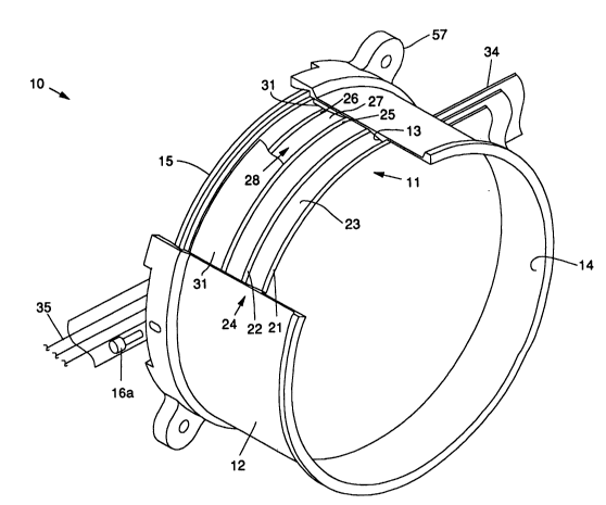
Referring to the drawing figures, Flg. 1 shows an assembled ele~ ,ui~ics pack-
age 10 in accordance with the principles of the present invention, while Flg. 2 shows
20 an exploded view of the d~;llvnics pAl`l~A~ 10. The ele~l,ul~ics pac~a~e 10 is shown
partially brûken away, thus illusll~u~g internal details of a circuit card stack 11 housed
therein. The elecllul~ics pAr~A~e 10 is co.. 'l" ;~e~ of a hollci~ 12 into which a plurality
of StA~`L'~ circuit cards 21, 22, 25, 26 co~l~ing the circuit card stack 11 are dispos-
ed, and which are l~tained in the housing 12 by means of a conical surface 13 that
25 forms part of an internal wall 14 of the housing 12, and a lock ring 15 and wedge-lock
,llechdnism 16.
First and second circular circuit cards 21, 22 are honded to a first heat sink 23
to form a first subA~-nhly 24. A conical angle is formed on the edge of the first
suh~cs~ -bly 24 that is adapted to mate with the conical surface 13 of the hollsing 12.
30 Third and fourth circuit cards 25, 26 are bonded to a second heat sink 27 and form a
second subacse nhly 28. An eYp~n~l~ble conical wedge ring 31 is provided that has an
intern~l angle that is adapted to wedge itself ~l. ~n the outer edge of the second sub-
~cs~nkly 28 and the intemal wall 14 of the ho~lcing 12. An el~ 1 inl~. r~S board
33 is provided that is PlP~ic~lly cQI-n~le~l to each of the circuit cards 21, 22, 25, 26.
35 Fxt~.rn~l connec!;ons are made by way of flat ele~i~l cables 34 or wires 35 as may be
chosen by the design~. A tapered lock ring 15 and wedge-lock ..~h~n;~.n 16 (com-
2 1 0 1 1 40
prising a screw 16a and a lock 16b) are provided to secure the colll~Jollerlk. in thehousing 12.
Assembling the electronics pae~ge 10 depicted in Fig. 1 is as follows. The
first circuit card 21 and the second circuit card 22 are i-~t~ol~n~teA and bonded to the
first heat sink 23 and form the first sub~cs~ .. bly 24. The third circuit card 25 and
fourth circuit card 26 are inte.~;o~-nec~A. and bonded to the second heat sink 27 and
f~m the second su~cs~-mbly 28. The first and second s~lb~sse.--blies 24, 28 are
col-nP~-te~1 using pin and socket or cclll~ ssion type contacts to form the circuit card
stack 11 which is placed into the houcin~ 12. The conical angle on the edge of the first
10 sub~c~embly 24 ~ng~es the mating conical surface 13 on the inner wall of the hollcing
12. The wedge ring 31 which has a radially located slot 32 (see Fig. 4) to allow for
co"~ ion and æ~ c:on, and a conical internal angle 38, is then slipped into the
hollcing 12, wedging itself ~Lw~.l the edge of the second sub~cs~ ~bly 28 and the
intem~l wall 14 of the houcing 12.
The electrir~l interf~oe board 33 COntaCb the top surface of the wedge ring 31
and makes el~ctric~ t~lcol-l~ ;on with the assembled circuit cards 21, 22, 25, 26,
using pin and socket type c~nt~rtc The pin and socket ~n~m~nt ~ sentati~e of
each of the cards 21, 22, 25, 26 is shown more clearly in Fig. 7. The lock ring 15 is
pocition~oA above the electnr~l int.~rf~re board 33 and has a wedge shaped slot 17 that
20 provides for eyp~n~ion and contraction to f.~ilit~t~ inst~ ti~n and co~ç~ssion lock-
ing. The lock 16b, which is activated with one screw 16a, engages the lock ring 15,
e~n-ling the ring 15 and forcing it against the negative conical surface 13a foqmed on
the inner wall 14 of the housing 12. This action causes downward ~l~ule that forces
the circuit card stack to seat and oenter itself into the ho..~ g 12 by eng~ g the first
25 heat sink 23 and conical surface 13, thus providing lll~ul.l "~hqnir~ n and
therm~l ~,sr~. When ll~ls~ e movement of the first heat sink 23 ceases, co~
eYr~nsion of the lock ring 15, foq~es a co~l~,ssion contact bel~. ~n conical surface of
the second heat sink 27 and the inner wall of the holl~in~ 12 through the lock ring 15,
similar to an eYr~n-ling collet. At a ~ t~,....;n~d point, when a specifi~ torque is
30 met on the lock screw 16a, the wedge ring 31, by e~ nd;ng, el;...;n~ s the tolerance
stack up, axially locates the c~uit card stack 11, provides a positive thermal path to the
housing 12, and provides the desired ~huClulal in~il~ for the electronics p~ ge 10.
For the pUI~O~S of clarity and ~ - , ' t~-ne~s, illustrations of the ~)one,lt
com~ ing the ele~ unics par~ç 10 will be 5lGs~ibe~ in greater detail. Flg. 3 is a
35 view of the lock ring 15 and wedge-lock n~ n;sm 16 employed in the cl~llunicsp~clr~ge 10 of Fig. 1. As can be seen, the wedge shaped slot 17 provides for expan-
sion and o~"n~ n of the lock ring 15 to f.~ilit~t~ in~t~ tion and c~l~l~s~i~n lock-
2tOt 140
ing. The lock 16b is eng~ed with a screw 16a that ~ ds the ring 15 by pulling the
lock with its oulw~dly tapered edges 18 to expand the ring 15 by exerting pl~ U~, on
similarly tapered inward edges 19 of the slot 17.
Fig. 4 shows the wedge ring 31 employed in the clc~ ~ics park~ge 10 of Fig.
S 1. The slot 32 in the wedge ring 31 that permits e~n~ion is more clearly shown. The
inte~n~lly tapered edge 38 of the wedge ring 31 is also shown.
Fig. S shows the f~rst heat sink 23 e~loy~ in the electronics pac~e 10 of
Fig. 1. The first heat sink 23 is shown having a conical outer edge 45 that matches the
taper of the conical surface 13 formed on the inner wall 14 of the housing 12. One slot
46 is shown that permit passage of a conne~;~r 47 that i~t~,r~onne~;l the first and second
circuit cards 21, 22.
Fig. 6 shows the second heat sink 27 employed in the electronics p~lra~ 10 of
Fig. 1. The second heat sink 27 is shown having a conicai outer edge 41 that eng~g~S
the conical edge 38 of the wedge ring 31. Four slots 42 are shown that permitpassage
of connectors 44 on the third circuit card 25 that illt~,lconnecl the third and fourth circuit
cards 25, 26 together.
Fig. 7 shows a typical circuit card that is ~ ~n~li~e of the circuit cards 21,
22, 25, 26 employed in the electronics p~ ge 10 of Fig. 1. The sets of COI n~cl-)r
pins 52 of the fourth circuit card 26 engage the cQnnectrlrs 44 of the third circuit card
25. Also, a C~ nl~e~;lor 49 of the fourth circuit card 26 conne~;l with col~n~1u~ 50 of
the int~ ce circuit board 33 (see Fig. 2). In a similar ll.a~, a set of connP,~b2r pins
51 of the third circuit card 25 engage a conn~rb2r 48 of the second circuit card 22 (see
Fig. 2). SimiLarly, a set of conne~lor pins 53 of the second circuit card 22 engage a
conneclol 47 of the first circuit card 21 (see Flg. 2).
Fig. 8 shows the housing 12 of the electronics pac~e 10 of Fig. 1, par~ally
broken away, showing detail of the internal co...~ ts thereof. The conical ~ ~ ri~r~s
13, 13a disposed on the inner wall 14 is shown more clearly. Mounting feet 57 are
shown as a means that permit ---~--n~ of the electronics p~ ~ 10 to a blllkhr~d for
~Y~mple~
Fig. 9 is a cross-section~l view of an ~c~e-mbl~d ele~ ,nics p~clr~ge 10. The
ihlle.~;on~e~ion of the various connectors and pins of each of the circuit cards 21, 22,
25, 26, and the i,.t,_l.;on,-~l;on of the fourth circuit card 26 to the elect ir~l in~- - r~ -e
board 33 is clearly shown. The mating of the conical angle on the edge of the first heat
sin_ 23 with the mating conical surface 13 on the inner wall of the housing 12 is more
clearly shown. Similarly, the wedge ring 31 is shown wedged ~l~n the edge of thesecond heat sin_ 27 and the internal wall 14 of the h~ ;ng 12.
2 ~ O 1 1 40
Fig. 10 is an enlarged sectional view of the assembled electronics package 10 ofFig. 9, çlnph~i7ing the .~ch~ni~ms that provide the unique locking and thennal trans-
fer aspects of the present invention. It more clearly defines how the lock ring 15 com-
presses the circuit card stack 11 when e~ a~-~ed into conical surface 13a of the housing
5 12 by ti~ht~ning the lock screw 16a
The high-density ele;l-o ~ics pac~ 10 may be used in ~lrJ~ace applir~tirn~
where ele ;ll~x~ic circuit cards must be packaged as a lightweight, highly LhPrm~lly con-
ductive, and ~I~ u ;~lly sound package. More speçific~lly, the present invention is a
unique p~aEing ~ng~mPnt for circular circuit cards, for example, that ...~ s
theImal L~ r~l from the circuit cards 21, 22, 25, 26 to the housing 12. The present
invention also provides e~ e~ rigidity, allowing the pacL~ 10 to pass rigid milita~y
mi~sion ~ uile~nb. This is achieved by bonding the circuit cards 21, 22, 25, 26 to
the heat sinks 23, 27 then positir~nin~ the sub~cse.nhli~s by the use of conical angles on
the edges of the heat sinks 23, 27 and the e pand~le conical wedge ring 31 colu~le
15 ed belween the conical ~r~.~es 13, 13a that both locates and locks the COLU~nenlS in
the hou~ing 12.
The high-density el~lloi~ics F~ e 10 provides an ~sembly for circular elec-
tronic circuit boards that achieves suitable themlal m~n~ .mt without the use of mis-
cellan~usP~litional h~-l~ . Theelecl icsp~ ge 10provides~ ;o thennal
- 20 ~ sr~,r capabilities, reduced circuit board flexing, which is eSpe~i-qlly advantageo~c
with HDM~ te~hnolQgy, and less weight than previous p~ ra~s, in~ lin~ card locks.
The p~qging and thermal managem~nt fe;~ s pr~vide heat sink 23 to heat sink 27
axial ali~m~nt regardless of tol~ role simplifying assembly, _nd provides
i.-l;."~le contact ~l~.~n the heat sinks 23, 27 and the holl$ing 12, and thus creating a
thermql path from the circuit cards 21, 22, 25, 26 to the houcin~ 12.
An emho~im~nt of a cyl;--~ ql high-densit,v ele~llunics p.lr~a,~e 10 has been
designeA built and tested, and S~ r;~s a need for a lightweight, thermqlly condu.;li~e,
and ~llu~;lul~lly sound elecll~,nics par~age The present invention provides a structure
that acl~i~ s these l~uil~nb, and also provides for greater service~bility, easier
fabric ,q,tion, faster assembly, lower cost and in.;l~d design lq-titl~de. ~il~ appli-
cations for the elecl-~ ics par~qge 10 are in the a~los~ace indus~Iy, although any app]i-
cation requiring the use of a plurality of stacked circuit boards opelal g in a hostile
en~nvr~lll would benefit from using the novel aspects of the present ele~ nics
a~ 10. The high-density el~unics parl~a~ 10 also provides for ~kuldald;~
and modlll~qri~y in space vehicle and missile ~esi~ for example.
The high-density cl~llonics p~r~q~e 10 provides for a ~u~- ;or design for
applications l~uilillg an easily asselllbled ele~ ,nics p~r~qg~ The use of wedge-
2101 140
shaped devices for locating and locking, instead of threaded fasteners, greatly enh~n~es
the servic.o~bility~ thd m~nagPm~nt and ~ of electronics p~c in which
they are employed. The electronics package 10 is easily f~hnc ~t~cl and required no
special tooling. Assembly of COIll~l~e.llS into the housing 12 is accomplished within
S n~;nu~ and ~lic~c~,mhly is equally fast and easy.
Thus there has been ~les~ihe~l a new and ~pno.~l high density ele~ unics
p~age having a plurality of stacked circuit boards that are heat sinked to the housing.
It is to be llntl~rstood that the ahove~es~ibe~ e."bo~;.. -~ is merely illu~la~ Of
some Of the many specific embo limentc which l~ ~nt applirationc of the prin i
10 of the present invention. Clearly, nu~el~us and other arrang~ can be readily
devised by those skilled in the art wi~l~ul de~ g from the scope of the invention.