Note: Descriptions are shown in the official language in which they were submitted.
2~:~
- 1 -
ADAPI ER FOR VIDEO AND AUDIO TRANSMISSION
Back~round of the ~vention
This invention relates to L, ~ n of video and audio b~
signals.
A present and future need exists to bring video and audio signals to the
desk, for e... r ~ ~ to provide security ~ .. ;ng factory pro~lnchon ll~nitolillg,
training, and video co.lf~ ..ci..g. Such i~fn. ~-- ~l;o~ needs usually require the
inc~~ll on of shielded wiring or optical fiber cables. It would be more e~ono. ., r ~1
to utilize wiring which is already available within the physical ~..c~ i.e., the~0 ~ln~hie1~l~ twisted pair cables used for ~ ,;on of analog voice signals.
r, a problem exists in p~ ~ing undue crosstalk between the video and
audio twisted pairs which are located within the same cable sheath.
Some vendors have ~ ,e:l t~ d applying video and audio signals to
hvisted pair by means of an active interface which shapes and ~n~ f ~ the signals
15 (see U.S. Pat. No. 5,130,793). IIo.._~e~, this a~l~ach is eA~hnsi~.,. It would be far
more ec~nc~ c-l to provide an adapter which will permit cour1ing of the video and
audio cl~ ~nf~1~ in a "passive" ratherthan an "active" manner.
Further, it does not appear that anyone has s~ggPs~ the appli~ion Of
dual channel audio signals to twisted pair wiring.
20 Summary of the Invention
The h-.- nUoll is a device for applying video and audio signals to a cable
inr lutling twisted pairs of wires. The device includes first and second ports for
coup1ing the device to a video and at least one audio channel. Each port is coupled
to a tra..~Ç~ ,f~ which has a high degree of balance. A third port is coupled to at
25 least one ~ r""..- ~, the third port being adapted for courli~ to twisted pairs of
wires.
Brief n ~of Ihe Drawin~
These and other features of the invention are ~f~ 'C~h d in detail in the
following ~1f ~ In the drawing;
FIG. 1 is a block diagram of a system inc1~ ;ng the device according to
one e~l of the in~ don;
FIG. 2 is a s~' ~ diagram of one portion of the device according to
the sarne c~ f ~
FIG. 3 is a S~ l'C ~ -~;C circuit diagram of the device in 7 'c Dr~nce with
35 the sarne e-..~;...~-n of the invendon;
21~1222
-2 -
FIG. 4 is an eYr'c~1ed pc.~p~;li~e view of a device in acc~ ce with
the same ~ , and
FIG. S is a plan view of a portion of the device in accur~lce with the
same e~
5 Detailed D~.;~,lion
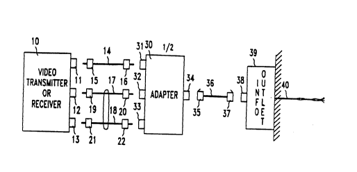
FIG. 1 il1vstr~q~tes the use of an adapter to permit t~ on of
~ ---ba ~~ video and audio signals on twisted pairs of wires. A video ~ n.;l~ . or
receiver 10 such as a VCR or TV camera includes an input/output for video signals
11 and a pair of inputs/outputs,12 and 13, for two channel audio signals. The video
10 1/0 11 is electrically coupled to a standard coaxial cable 14 which is ~ ~ ~ by
standard BNC plugs 15 and 16. Each audio l/O, 12 and 13, is electrir~lly coupled to
a stand. rd audio cable with wires 17 and 18, ~ ..;n~t. .d in standard phono plugs, 19,
20 and 21, 22, ~ 1y.
An adapter 30 includes a first set of ports, 31, 32,33, which are standard
15 recep~q~ 1~s for l~cei~ng and electnc~lly ~ ~g,~ the plugs 16, 20, and 22 of the
cables 14, 17 and 18. At the other end of the adapter is an output port, in thisexample a single modular jack 34, which is adapted for l-i.,e;villg and el~ctricqlly
e n~ ;ue a standard modular plug 35. That isy the modular jack 34 includes at least
three pairs of ele~;tl;cdl pins, each pair coupled to one of the input ports, 31-33. In
20 this ~ . !e, a standard 8-pin modular jack is employed with the pin layout
inllstrq-ted in FIG. 2. As shown, the first two pins (1 and 2) are used for audio
channel "A", while pins 3 and 6 are used for audio channel "B". Pins 7 and 8 areused for the video channel. Pins 4 and 5, normally used for voice tral~c-~ L:o~ are
not used by the adapter. (l;or an example of a standard 8-pin modular jack, see,25 S~. ~Y~9P,~ og DistributionSystemCa...,-o.~ ~ Guide, AT&TDoc.
No. 3726C, p. 3-10, ~vCe-~ l 19903.)
Cord 36, which can be a standard ~ P11ed twisted pair cord
cor ~ e at least three twisted pairs, includes a similar plug 37 at the end opposite
to the plug 35. The plug 37 mates with a modular jack 38 which is part of the
30 infnrm~tion outlet 39 mou d to the wall of a building. This information outlet
couples the video and two audio signals onto separate twisted pairs of a four-pair
cable, 40, which rans lh~-Jughoul the building. The inl~ ;nn outlet 39 is a
standar~ part of an AT&T S~ h~ iSCS Distribution System. (See, for
e , 'e, Cl..7J.JI.~nt~ Gufde, cited above.)
21~1222
- 3 -
In order to permit the audio and video signals to be h~ t~ over the
four twisted pairs which share a cc.. ~ sheath, the adapter 30 is con~lu-,t~d ina ~ - e with the circuit - ~ ' - diaglam of FIG. 3. Port 31, which receives the
video channel signals, co...~ es, in this c-~ho~ - nl a standard BNC female
S coaxial cr ~ 'o., but could be any suitable c.,nnf.to(. The signal portion of the
con~ ~. is coupled to one end of the primary winding of first 1, t~ U~ T I,
while the ground portion ûf the CO~ f,~ is coupled to one end of the secQn~
winding of trall ~ru~ T l - The opposite ends of the windings are coupled to the
~ r ~ t~ pins (7 and 8) of the modular jack 34.
The ports 32 and 33, in this - ~1e7 CV"'1~;Ce standard phono jacks.
The signal portion of each jack is coupled to one end of the primary winding of an
A~s~:--tA ~ ru. .. - , T2 and T3, while the ground co.~.-f~ion of each jack is
coupled to the other end of the primary winding of its A~SOC :~t~ r ~'f .. ~- ' . The
s~,cs~ windings are coupled to the a~ u~lidlt; pins (6, 3, 2 and 1) of the modular
15 jack 34. As ~ ;viOlisly ...r:i~1;r~neA pins 4 and 5 of modular jack 34 are not used in
this e-.-ho l;".f Al
The ~I n ~rv~ , T I - T3, have certain ch.u ;,- h-; '1;~'5 to pr~duce low
crosstalk between the audio and video signals. A high balance, i.e., tight coupling
between the two win~ing, of the ~ .rc....le~, is required. In particular, it is
20 de;.ll '~' - that the videv ~. ,...~rc~ cr~ T I, have a common mode ~ej~lion greater than
4û dB for r.~ kf s up to 50 MHz. The audio LI~Ç~ should have a cc,.. on
mode rejection greater than 40 dB for rl~u -~ 5 Up to 100 kHz. This high balancecan be .~lL'.~, ~ed, for e . 1 , by means of a "bifilar" winding al. .v~g~ wherein
both primary and s ~ . i..Lng;, are wound side by side a~ound a
25 core. Such a winding ..~ -;, leakage ;~ e, and DC ~ ce lirre..,.lces
between WilldiJ.~ in or~er to allow for the high degree of balance.
A flat fi~u~,n~,y ~5iSI~u~ G for each 1l. r iS also ~ ,k~l~ tO
a~ ,Iy ~luduce the video and audio signals at the output port (34) of the
adapter. It is, Ihe.efo~e, I~-O~ that the rl~u~ IC~ of the video
30 tra.,,fo,l,le. be within + 0.5 dB in the DC to 8 MHz L~e.l.;y range, while the
r,~uc.l~ iapl~ of the audio l~ rolllJ.,.~ be within i O.S dB in the S0 Hz to 15
kHz L~ue.l~ range. It is further desirable for the ~.,.. ~r.. - ~ to exhibit low loss
to ensure that the video and audio signals are not unduly ~Ih~ t~ A A loss of nogreater than O.S dB is desirable. In order to achieve such losses, a ..-~ core
35 material with a high pemlP~hility is .~,cc.. ,~ n-l~l for each 1l,~ r"" ". ~. In this
2~ 2~
-4-
.
example a p.,....~ i1ity of 20,000 was used, but in general a ~v. l~ 'lity of greater
than lO,000 is desirable.
~ ;IGS. 4 and 5 illustrate one example of a physical e, .~ t of theadapter 30. The BNC coaxial co~-n~t.... 31 includes a post 50 which mounts the
S co~ ~- onto a printed circuit board Sl by soltl~ g four legs of the post into holes
(61-64 of FIG. 5) in the bo_rd. The signal portion of the contact is soldered inhole 65. Phono jacks 32 and 33 are e ' ~ 'ly attached to inc~l- ing blocks 52
and 53, lb~ev~ ly, which are snapped into holes (66, 67 and 68, 69, ~ ely)
in the circuit board. Do....~.~uvUy e-l~ nr1;~g vertica1 posts (no~ shown) which are an
lO integral part of the cnnn~ctn~ 32 and 33 and couple the ground and signal portions
to the board are soldered in holes 70, 71 and 72, 73 Iv;,~ vly, in the circuit board.
It will be noted in regard to FIG. S that each ....~ ,g posidon for the
contacts includes the same array of nine holes so that the po~ lin.~c and types of
contacts can be varied if desired.
Each col-l-e~ I ~ is coupled to its ~csc - ~ d tran~ vr (T I - T3) by
means of convlu~ v leads, e.g., 75, forrned on the bottom surface of the printedcircuit board. Each ~ r,.,.". ,, in turn, is coupled to its A~S~ 1 pins of moc1ular
jack 34 by con-lu~ v leads, e.g., 76, which are also .1~ ~,os;t~ d on the bottom surface
of the printed circuit board. The pins of the modular jack 34 are soldered in their
20 lv~clivv holes, e.g., 77.
The circuit board 51 and the Cc~ e~t' ll_ ~ thereon are enc1ose~
within a housing formed by two half-shells, 80 and 8l, n..~cl.~ic~11y attachecl by
means of four posts (82-84 being visible) fitted within c~llr~ nlling holes (85-87
being visible).
It will be ap~lr~;&tvd that it should be possible to also include voice
signals on one of the twisted pairs within the same sheath as the pairs carrying the
voice and audio signals in the cable (40 of FIG. l)
Various ."~l;~r~;onc of the in~ lio,l will become apparent to those
skilled in the art. All such variations which basically rely on the ~ .g~ through
30 which the in~ r has a.lvanc~d the art are ~ / conside.rd within the scope of
the in~_ntion.