Note: Descriptions are shown in the official language in which they were submitted.
2 ~ 2 ~ ~
TITLE OF THE lNv~h~lON
Nethod of Forming Single-Cryst~lli n~ Thin Film
RA~RG~UND OF THE lNV~ lON
Field of the Invantion
The present inve~tion relates to a method of forming
a single-crystalline thin film on a base material, and
more particularly, it relates to a method for forming a
single-cryst~lline thin film consisting essentially of an
oxide superconductor on an arbitrary base material.
~hroughout the specification, the term "single-
cryst~lline" means a d~ in~tive state of a crystal having
a specific orientation. This term is applied not only to
a single crystal having only a sperif1c orientation but to
a cryst~lline solid cont~ining a mixture of crystals
having different orientations with a ~ n~tive state of a
crystal having a specific orientation.
Descrip~ion of the Background Art
In a technique of fabricating a semiconductor deviee,
various methods such as liquid phase epitaxy (LPE),
org~n~ -Lallic chemical vapor deposition ~MOCYD),
molecular beam epitaxy (MBE) and ion beam epitaxy (IBE)
are employed as methods of forming thin films of
semiconductor single c.rystals. These methods, which are
capable of forming high quality single-crystalline thin
films, are indispensable techniques for fabrication of a
-- 1 --
2 g 3
~emiconductor device.
In the field of superconduction, methods of forming
single-crystalline thin films have been studied since
discovery of ~, Bi and Tl oxide superconducting materials
having critical temperatures of 90 K, 108 K and 125 K
which are higher than the liquid nitrogen temperature of
77.3 R, in order to apply these materials to electronic
devices. It has been found tha~ methods such as laser
vapor deposition, reactive vapor deposition and the like
are effective for forming high quality single-crystalline
thin films with respect to such oxide ~upercon~cting
materials.
The aforementioned conventional methods of f~ i ng
single-cryst~lline thin films utili~ing epitaxy, i.e.,
such a rh~n~ on that another type of crystal is grown on
a speci~ic crystal plane in a constant orientational
relation, are generally adapted to form thin films on
surfaces of single-crystalline sub~trates. In each of
such conventional methods, it is extremely ~ Lant to
employ a single-crystAlline substrate having a crystal
structure and a lattice constant which are si ilAr and
close to those of the thin film material, in order to form
a high quality single-crystalline thin film. In such
prior art, therefore, a single-crystalline thin film can
be formed only on a substrate which is made of a specific
2 ~ ~
material, while the size of the formable single-
cry-stAll;ne thin film depends on that of the employable
substrate. Thus, it is impossible to freely form a
single-crystalline thin film having desired size and
S length according to the prior art.
In the field of a semiconductor thin film, on the
other hand, there is graphoepitaxy of employing an
amorphous substrate having periodic grooves formed on its
surface and generating crystal nuclei on edges of these
grooves in a selective orientation, thereby single- -
crystallizing a film deposited on the substrate.
According to this technique, it is possiblq to form a
single-cry-stalline thin film having excellent
cry-stallini~y as to Si, for example, without employing a
single-cryst~lline substrate. Also in such graphoepitaxy,
however, the size of the substrate which can be provided
with periodic grooves is restricted. Thus, it is
difficult to freely form a single-crystalline thin film on
a base material having desired size and length, si~i l~rly
to the above.
In recent years, ther has been made an attempt of
forming an oxide superconducting film on a flexible long
tape base material for manufacturing a superconducting
wire. The base material for the wire is generally
prepared from a metal, which is a polycly3~alline
21~2~5
substance in general. When an oxide thin film is formed
on such a base material by laser vapor deposition or
reactive vapor deposition, generally formed is a
poly~lyslAlline or amorphous thin film having random
orientation. Even if the thin film has natural
orientations, crystals forming the thin film orient
specific crystal axes in a direction ~e.~andicular to the
surface of the base material, while hardly orienting axes
in a direction parallel to the base material surface.
Also when an oxide superconductor film is formed on a
poly~ly~LAlline substrate of MgO, SrTiO3 or ZrO2, the as-
formed film has irregularly oriented crystal planes.
Since a superconducting current is i nh i hi ted by grain
boundaries, it is impossible to attain sufficient
superconductivity in a thin film which is formed on a
poly~ly~Lalline substrate by the prior art.
SUMMARY OF THE lNv~hl~ON
An object of the present invention is to provide a
method which can form a single-crystalline thin film
having excellent crystallinity on a base material without
depending on a material for and crystallinity of the base
material.
Another object of the present invention is to provide
a method which can arbitrarily form a single-crystalline
thin film having excellent crystallinity on a base
21 ~28~
material of a desired size.
Still another object of the present invention is to
form an oxide superconducting thin film having excellent
crystallinity and superconductivity on a poly~ly~Lalline
base material.
A further ob~ect o~ the present invention is to form
an oxide superconducting thin film having excellent
crystallinity and superconductivity on a long base
material, thereby fabricating a wire which P~h i hi ts a high
critical current density.
Provided according to the present invention is a
method for forming a single-cryst~ ne thin film which is
mainly formed of a crystal having a specific orientation,
more preferably a thin film of a single crystal, on a
continuous region of a base material from a vapor phase.
~his method compxises a step of preparing a base material
to be provided thereon with a thin film, a step of
preparing a vapor phase for depositing a crystal on the
base material, a step of covering the base material with a
mask which can ~L~vent chemical species contained in the
vapor phase from adhering to the base material, and a step
of relatively moving the base material with respect to the
mask thereby continuously delivering a portion of the base
material having been covered with the mask into the vapor
phase.
s2,~2~5
The present invention is adapted to form a single-
crystalline thin film consisting essentially of an oxide
superconductor, more preferably a thin film of a single
crystal, on a base material, in particular. The oxide
superconductor includes a Y-based superconductor such as a
Y-Ba-Cu~O superconductor, a Bi-based superconductor such
as a Bi-Sr-Ca-Cu-O superconductor, or a Tl-based
superconductor such as a Tl-Bi-Sr-Ca-Cu-O superconductor.
The vapor phase for depositing the oxide superconductor
can be prepared in accordance with vapor deposition such
as reactive vapor deposition, laser ablation, molecular
beam epitaxy (MBE), CVD, ion plating, spray pyrolysis,
flash plasma or the like. When laser ablation is
employed, it is possible to form a single-crystalline thin
film of a superconductor by irradiating a target of a Y,
Bi or Tl have sintered body with a laser beam for
generating plasma and exposing a base material delivered
from the mask to this plasma. A substrate for forming a
thin film of an oxide superconducting material has been
generally prepared from a single crystal of MgO, SrTiO3 or
ZrO2. According to the present invention, however, a base
material can be prepared from a polycrystalline material
of MgO, SrTiO3 or ZrO2, a sheet of yttria stabilized
zirconia, or a metal base material such as a metal tape,
in addition to the said material.
-- 6 --
2'1 ~
The present invention is applied to formation of a
single-crystalline thin film on a poly~Ly~Lalline
substrate, in particular.
The foregoing and other objects, features, aspects
and advantages of the present invention will become more
apparent from the following detailed description of the
present invention when taken in conjunction with the
acc~ nying drawings.
BRIEF D~SCRIPTION OF THE DRAWINGS
Figs. l~a) to l(c) are perspective views typically
showing an exemplary process of forming a thin film
according to the present invention;
Fig. 2 is a plan view showing another exemplary
process of forming a thin film according to the present
invention;
Fig. 3 is a model diagram showing a process of
forming a single-crystAlline thin film on a base material
which is previously provided with a metal thin film
according to the present invention;
Fig. 4 is a sectional view showing a state of the
metal thin film formed on the base material in the process
shown in Fig. 3 in an enlarged ~nner;
Fig. 5 is a perspective view for illustrating a
process of forming a single-crystAl~;ne thin film while
feeding a gas in a prescribed direction;
21~2~
Fig. 6 is a perspective view for illustrating a
process of forming a single-crystalline thin film with
irradiation of a laser beam or an ion beam;
Fig. 7 is a ~ectional view showing a process of
forming a single-crystalline thin film in Example 1
according to the present invention;
Fig. 8 is a model diagram showing a ~tate of f-_ i ng
a single-crystalline thin film by laser ablation in
Example 2 according to the present invention;
Fig. 9 is a model diagram showing a state of forming
a single-crystalline thin film in Example 11 according to
the present invention;
Fig. 10 is a plan view for illustrating a process of
forming a single-crystalline thin film in E~ample 13
according to the present invention;
Fig. 11 is a perspective view for illustrating a
process of forming a ~ingle-crystalline thin film in
Example 14 according to the present invention; and
Fig. 12 is a sectional view for ~ypically showing a
process of forming a single-cryst~lline thin film in
Example 20 according to the present invention.
DESCRIPTION OF THE PR~FERRED EMBODIMENTS
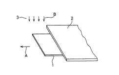
Figs. l(a~ to l(c) are pexspective views typically
showing a process of forming a ~hin film according to the
present invention. According to the present inven~ion, a
-- 8 --
21~-~2~3
base material 1 is delivered into a vapor phase 3 for
crystal growth from an end thereof through a mask 2. This
base material 1 is delivered along arrow A in Fig. l(a).
On the other hand, chemical species cont~ine~ in the vapor
phase 3 are deposited on the base material 1 as shown by
arrow ~ in Fig. l(a). As shown in this figure, no
chemical species contained in the vapor phase 3 adhere to
a portion of the base material 1 covered with the mask 2,
while the chemical species adhere to a portion delivered
into the vapor phase 3 from under the mask 2. Thus, a
thin film is continuously formed on the base material 1,
which is continuously delivered along arro~ A.
Description is now made on a process of foxming a
single-crystalline thin film by moving the base material
1. For the purpose of illustration, it is assumed that
the base material 1 is delivered from such a state that an
end thereof is slightly exposed to the vapor phase 3.
Fig. 1(b) shows a certain point of time during delivery of
the base material 1 from the state shown in Fig. 1(a). A
region la of the base material 1 has been exposed ~o the
vapor phase 3 in advance of such ~/v. --t of the base
material 1, with no experience of v. t from under the
. mask 2 into the vapor phase 3. In such a region la, a
thin film formed on the surface of the base material 1 is
generally formed by crystals having random orientations or
2~
in an amorphous state. Even if the thin film has natural
orientat.ion, crystals forming this film orient specific
crystal axes in a direction normal to the surface of the
base material 1, with less implementation of a specific
orientation in parallel with the base material surface.
In a moved region between the region la and the mask 2, on
the other hand, an initial portion lb is influenced by the
,- -,ved region la to form crystals having various
orientations. Following the -v~ --t, however, a certain
specific crystal orientation becomes so d~ ;n~nt as to
form a region lc having a regular orientation. Referring
to Fig. l(b), arrows show a distributed state of crystal
orientations, in order to typically illustrate such a
state. This is conceivably because a crystal growth end
is formed on a boundary region between the portion of the
base material 1 which is covered with the mask 2 and that
which is exposed to ~he vapor phase 3, so that a crystal
having the same orientation as the growth end is grown on
the portion of the base material 1 newly exposed by its
~v --t. When a growth end having a specific crystal
orientation can be reliably grown, therefore, it is
possible to form a thin film having strong single
cryst~ll;n;ty with no remarkable influence by the material
for and the crystal orientation of the base material 1.
When the base material 1 is further moved in the
-- 10 --
2~ ~ 28~
aforementioned nn~rr the crystal having the same
orientation as the region lc is further grown as shown in
Fig. l(c). Once grains having a specific orientation are
dominatively formed as hereinabove described, crystal
grains having the specific orientation are continuously
formed on the base material 1 by continuous -v. --t
thereof and an effect of the mask 2, with no regard to the
material for and the crystal orientation of the base
material 1.
When a tape-type base material is employed in the
aforementioned method and moved along its longitudinal
direction from one end thereof, for example, it is
possible to form a single-crystalline thin film over the
longitudinal direction of the base material.
When a base material 11 is covered with a mask 12
having a window 12a as shown in Fig. 2 and vapor
deposition is carried out from above the window 12a, it is
possible to form a thin film only on a portion of the base
material 11 located under the window 12a. If the base
material 11 or the mask 12 is continuously moved in this
state, it is possible to form a thin film on a region lla
(shown by one-dot chain lines in Fig. 2) along which the
window 12a is moved. Also in this case, it is possible to
form a single-crystalline thin film on the region lla due
to the aforementioned continuous ~"ove...cnt and the effect
- 11
2 1 0 1 2 ~ ~
of the mask 12. When such a mask 12 is employed, it is
possible to form a single-crystalline thin film on an
arbitrary region of the base material 11.
According to the present invention, the base material
can be prepared from an arbitrary material in an arbitrary
shape. The material and the shape of the base material
can be properly det~ ine~ in response to the application
of a substance obtained by forming a single-crystalline
thin film, film forming conditions, and the like. The
method according to the present invention is applicable to
formation of a single-crystalline thin film on a long base
material such as a tape-type base material, in particular.
According to the present invention, the mask for covering
the base material is not restricted so far as the same can
prevent chemical species for vapor deposition from
adhering to the base material, and the material, the shape
etc. thereof may be properly selected in response to the
film ~orming conditions and the like. This mask must be
so provided as to effectively prevent chemical species
contained in the vapor phase from being scattered on the
base material. When the base material is covered with the
mask, therefore, it is necessary to ~l~vent molecules,
atoms etc. for vapor deposition from entering a clearance
between the mask and the base material. To this end, a
distance between the base material and the mask is
- 12 -
2 ~ ~
preferably not more than about 3 mm when vapor deposition
is employed, although this distance depends on conditions
for vapor-phase growth. According to the present
invention, the base material is relatively moved with
respect to the mask. Namely, the base material is moved
when the mask is fixed, and vice versa. Alternatively,
both of the mask and the base material can be moved at the
same time. In order to form a single-crystalline thin
film on a tape-type base material, for example, a mask may
be fixed so that the tape-type base material is
continuously delivered into a vapor phase for crystal
growth through the mask. Since such a tape-type base
material can be taken up, it is possible to deliver the
tape-type base material from a first reel into a vapor
phase for crystal growth through a mask while taking up
the same on a second reel, thereby successively forming a
single-crystalline thin film on the tape. As hereinabove
described, it is also possible to cover a base material
with a mask which is provided with a window such as a
slit, so that chemical species contained in the vapor
phase adhere to the base material through the window.
When the base material or the mask is so moved that the
window passes through the base material, it is possible to
form a single-crystalline thin film on a portion of the
base material through which the window has passedO
- 13 -
21~283
According to the present invention, an environmental
phase for crystal growth is a vapor phase, so tha~ PVD
such as sputtering or CVD can be employed for vapor-phase
crystal growth. According to the present invention, laser
vapor deposition, reactive vapor deposition,
organometallic chemical vapor deposition (MOCVD),
molecular beam epitaxy (MBE) or ion beam epitaxy (IBE) is
preferably employed as a vapor phase growth method, for
example.
In a more pre~erred mode of the present invention, it
is possible to form a thin film which is mainly formed of
a crystal having a speclfic orientation on.a continuous
region of a substrate from a vapor phase which is prepared
along laser ablation. In this case, a portion of a base
material which is covered with a mask is more preferably
delivered at a speed of at least about 1 cm/min. into the
environment for crystal growth when the base material is
relatively moved with respect to the mask. When an oxide
superconductor film is formed, laser ablation can be
carried out under conditions of a base material
temperature of 650 to 750~C, a gaseous oxygen pressure of
30 to 500 mTorr, a laser beam in a wavelength region of
248 to 1060 nm and a laser energy density of 1.5 to 3.3
J/cm2 .
In order to control the orientation of a crystal
- 14 -
2~ 3
which is formed on a growth end, the following technique
is preferably employed:
As shown in Fig. 3, it is possible to form a single-
crystalline thin film by employing a base material 21
which is previously provided with a metal thin film 20 and
providing a temperature gradient in a boundary region
(denoted by C in Fig. 3) between a portion of the base
material 21 which is covered with a mask 22 and that which
is exposed to a vapor phase 23. The temperature gradient
can be set by a heater 24 which is provided under the base
material 21, for example. Cooling means may be further
provided for temperature control. The metal thin film is
made of a material which can be evaporated in the vapor
phase. Due to the as-set temperature gradient, the metal
thin film has a solid-liquid boundary at the boundary
region C. Fig. 4 shows a state of such a solid~liquid
boundary in an enlarged manner. As shown in Fig. 4, a
portion 21a of the metal thin film 20 covered with the
mask 22 is left in a prescribed thickness while another
portion located in the boundary region C is melted to form
the solid-liquid boundary and the metal forming the thin
film 20 is evaporated in this portion fr~m a high
temperature part. Consequently, the portion of the metal
thin film 20 located in the boundary region C is eroded to
exhibi~ a stepped shape. Such a state can be observed
- 15 -
21 01 28~
with an electron microscope. When a silver thin film was
formed on a base material, for example, it was clarified
by observation with an electron microscope that steps were
defined in correspondence to a temperature contour line
with a height of about 100 A and a terrace width of about
looo A in each step. When a mask is so provided that a
film forming region is interrupted, i.e., a crystal growth
end is defined in a region provided with such steps,
chemical species deposited from the vapor phase generate
nuclei with a regular orientation along corners of the
steps. When the base material is continuously msved along
arrow shown in Fig. 3, steps of the metal thin film are
regularly formed in the region provided with the
temperature gradient and hence the thin film is grown with
lS a regular orientation along the corners of the steps.
Consequently, a single-cryst~lline thin film is formed in
a continuous -nn~r. Such foxmation of a thin film with a
temperature gradienk is applicable ~o a single-crystalline
thin film which is formed along a longitl-~in~l direction
of a tape-type base material, or a single-crystalline ~hin
film which is provided on an axbitrary region of a base
material covered with a mask having a window. In order to
foxm an oxide superconducting thin film, a silver thin
film is preferably employed as a metal thin film.
According to the present invention, it is possible to
- 16 -
~al2~3
supply a portion of a base material, which is released
from coverage with a mask and delivered into environment
fox crystal growth, with a gas flow of the same direction
as that of relative v. --t of the base material by
feeding a gas along the said direction. Such a gas flow
can be formed by generating the gas from a slit-type hole
which is provided on an end of the mask toward the
envilor~ nt for crystal growth, for example. When a gas
34 is fed along a direction (shown by arrow D) of mov,~ ~nt
of a base material 31 from an end 32a of a mask 32 as
shown in Fig. 5, for example, it is possible to grow a
crystal having a specific orientation on a.region of the
base material 31 holding directionality of such a gas flow
along this direction. ~he region holding directionality
of the gas flow is conceivably restricted to an extremely
narrow range. Once a thin film having a regular
orientation is formed on this portion, however, it is
possible to form a film along the orientation of the
underlying film which is formed along the gas flow even if
this film is formed on a region, such as a portion
separated from an injection port for the gas, bre~king the
directionality of the gas flow. Also in a case of forming
a thick film, there~ore, it is possible to grow a crystal
having a specific orientation by regulating its
orientation along the underlying film whose orientation is
2 ~ ~
controlled by the gas flow. Thus, the gas flow so serves
as to form a crystal nucleus having a specific
orientation. Nhen the base material is continuously moved
to successively expose the region covered with the mask to
the vapor phase, growth of a thin film progresses so that
its orientation is regulated along the crystal which is
controlled in orientation by the gas flow, as hereinabove
described. Thus, it is possible to form a single-
crystalline thin film having a regular crystal orientation
on the base material. Such formation of a thin film using
a gas flow is applicable to a single-crys~l1ine thin film
which is formed along a longitt~ln~l directio~ of a tape-
type base material, or a single-crystalline thin film
which is formed on an arbitrary region of a base material
covered with a mask having a window. In order to form an
oxide superconducting thin film, the gas preferably
consists essentially of oxygen.
As hereinabove described, it is possible to further
positively control the crystal orientation by using a
metal thin film or a gas flow. However, it is rather
difficult to stably obtain a proper solid-liquid interface
by optimizing temperature distribution on a boundary
region, due to slight fluctuation in a distance between a
base material and a heating apparatus or the like.
Further, specific and fine adjustment of a gas nozzle is
- ~8 -
2 ~ ~
required in order to supply the base material with a
constant gas flow. The aforementioned technique requires
complicated adjustment and operations, with difficulty in
maintenance of a proper state for a long time. To this
end, the inventors have found a method of using a laser
beam or an ion beam as shown in Fig. 6, in order to carry
out stable control for a long time. Referring to Fig. 6,
a boundary region 35c between a portion 35a of a base
material which is covered with a mask 36 and another
portion 35b which is exposed to a vapor phase 37 is
irradiated with a linearly focused beam 38. This beam 38
is prepared from a linearly focused laser beam or an ion
beam having a linear section. Due to irradiation with
such a beam, it is possible to relatively easily implement
an extremely higher energy state in a boundary region as
compared with a peripheral portion. E~en if molecules or
atoms entering a small clearance between a mask and a base
material come into contact with a portion of the base
material, being covered with the mask, which is close to a
boundary region to form a polycrystalline initial thin
film, therefore, such an initial thin film is completely
evaporated from the base ma~erial or sputtered (worn) at
the boundary region when the base material is continuously
delivered from the mask. Thus, the surface of the base
material is maintained in high purity. Film formation on
- 19 -
S~ 2 ~ ~
the base material is first started ~ tely after ths
base material is released from irradiation with the laser
beam or the ion beam. Consequently, shape steps having
excellent reproducibility and a regular crystal
orientation are formed on the base material so that an
initial growth film is formed along edges of such steps.
Since an initial growth film having a specific crystal
orientation is reliably formed in ~he aforementioned
manner, it is possible to thereafter grow a film with a
d~ in~tive crystal orientation also at a position
separated from the boundary region. According to this
technique, there~ore, it is possible to form a thin film
having a regular crystal plane orientation on a base
material without forming a solid-liquid interface in a
boundary region between a mask and a base material and
without supplying a gas ~low in a direction of relative
v~ - t of the base material. The laser beam is
preferably prepared from a coherent pulsed laser beam such
as an excimer laser beam. The beam source can be selected
from ArF, KrF, XeCl and N2 excimer lasers, and a YAG laser.
The excimer lasers have specific oscillation wavelengths
of 193 nm, 248 nm, 308 nm and 337 nm respectively. As to
the YAG laser, it is possible to preferably use second,
third and fourth h~ ~/nics. When an oxide superconducting
film is formed, an excellent result can be obt~ine~ by
- 20 -
21~12~
setting an energy density of the pulsed laser beam in a
range of at least 0.5 J/cm2 and not more than 5.0 J/cm2
per pulse. The pulsed laser beam can be l; ne~rly
converged through a cylindrical lens or a cylindrical
S mirror. On the other hand, an ion beam can be obtained by
accelerating and converging ions generated from an ion
source with an electrostatic lens system, as is well known
in the art. The boundary region of the base material is
irradiated with the ion beam having a l ine~r section under
conditions required for implementing a high energy state
by acceleration of ions and an effect of charges.
Dispersion of energy distribution is preferably not more
than 5 ~ on a section of the ion beam. An ion source may
be prepared from argon, oxygen or a mixture thereof, for
example. The energy of the ion beam can be set in a range
of 50 to 500 eV, for example. Such irradiation with the
beam can be c~ ';ne~ with the aforementioned technique of
employing a metal thin film or a gas flow.
As described in the following Examples, the present
invention is preferably employed for forming a thin film
which consists essentially of an oxide superconductor on a
flexible long base material. An oxide superconductor film
having excellent cryst~lli n; ty provides a wire having
excellent superconductivity. The present invention is
also applicable to fabrication of a superconducting
- 21 -
element. As to the aforementioned technique employing a
beam, expected is application to fabrication of a long
wire such a~ a wire of at least 100 m, for example.
Example 1
An Ni-Cr alloy tape of 0.1 mm in thickness and 5 mm
in width was employed as a base material 41, and a mask 42
of stainless steel was fixed on this base material 41 with
a clearance d of 0.1 mm as shown in Fig. 7. Reac~ive
vacuum deposition was employed for forming a thin film of
yttria stabilized zirconia on the Ni alloy tape. A
reaction gas was prepared from oxygen, and its pressure
was set at 3 mTorr. The temperature of the base material
41 was set at 750~C. As hereinabove described, the base
material 41 was continuously moved along arrow E in Fig. 7
at a speed of 2 mm/min., to form a thin film of yttria
stabilized zirconia by vacuum deposition. At this time, a
portion of the tape up to 5.2 cm from its front was
provided with a non-oriented thin film of yttria
stabilized zirconia, while a subsequent portion was
provided with a lm; A~; A~ ly oriented film perpendicularly
directing its [100] axis to the surface of the base
material 41 over a length of 3.8 cm. A further subsequent
portion was provided with a thin film of yttria stabilized
zirconia strongly orienting [010] and [001] axes in a
plane parallel to the base material surface with a regular
- 22 -
orientation of these axes within an inclination of 5~. It
was confirmed by ~-ray diffraction that this orientation
(biaxial orientation) was implemented over a length of 3
m. Also as to another length, it was anticipated that a
thin film having a strong biaxial orientation, i.e., a
single-crystalline thin film, can be obtained so far as
conditions for vacuum deposition and continuous ~,v~ -nt
of the base material are stable and the mask is provided
in a fixed manner.
Example 2
The same Ni-Cr alloy tape as that in Example 1 was
employed as a base material 51, to form a thin film of
yttria stabilized zirconia by laser ablation. The laser
ablation was carried out as shown in ~ig. 8. A target 54
of a Y sintered body was irradiated with a laser beam 55
to generate a plume 56 shown in Fig. 8 in a direction
perpendicular to the target surface, so that chemical
species contained in the plume 56 adhered onto the base
material 51 which was continuously delivered from above
the mask 52. In such laser ablation, the temperature of
the base material 51 was set at 650 to 750~C, and gaseous
oxygen was set at a pressure of 30 to 500 mTorr. The
laser beam 55 was emitted from a KrF excimer laser
(wavelength: 248 nm), with a laser energy density of 1.5
to 3.3 J/cm2 and a laser repetition rate of 1 to 100 Hz.
- 23 -
2 ~ 8 ~
A clearance d between the base material 51 and the mask 52
was set at 0.1 mm. Also when such laser ablation was
employed, it was possible to form a thin film of yttria
stabilized zirconia having strong single-crystAllinity
S over a length of 2 m from a portion of 12.5 cm from the
front of the tape-type base material 51.
Example 3
The same base material as that in Example 1 was
employed to form a thin film of yttria stabilized zirconia
through no mask. The as-formed thin film, in which [100]
and ~111] axes were uprighted with respect to the base
material surface in ~ mixed state, ~hihited random axial
orientation with respect to the direction in the base
material surface. Then, a Yl~a2Cu3O~ thin film was formed
according to the present invention on the thin film of
yttria stabilized zirconia formed on the base material
through laser ablation shown in Fig. 8. In this laser
ablation, gaseous oxygen was set at a pressure of 200
mTorr, ~he base material was set at a temperature of
700~C, and a film forming rate was set at 1.5 ~m/min. A
laser beam was emitted from an excimer laser similarly to
Example 2, and the base material was continuously moved at
a speed of 18 mm/min., to continuously form the YlBa2Cu3Ox
thin film. The as-formed thin film was c-axis oriented
along the overall tape length, while a and b axes
- 24 -
2 11 ~.2~
exhibited strong orientation from a portion of 5.6 cm from
the tape front and it was confinmed that the orientation
of these axes was within 4~ over a length of 1.4 m.
Example 4
A tape-type base material provided with a thin film
of yttria stabilized zirconia having strong single-
c.rystallinity formed in Example 2 was prepared in a length
of 1 m. Then, a YalBa2Cu3O~ thin film was formed through a
mask by laser ablation similarly to ~xample 3, under
conditions of a base material t ~_lature of 700~C, a
gaseous oxygen pressure of 200 mTorr, a film forming rate
of 1.5 ~m/min. and a base material moving speed of 18
mm/min. In this case, a c-axis oriented film having
strong single-crystallinity was formed from a portion of 8
mm from the tape front. In this film, a crystal axis
which was substantially parallel to the base material
surface was oriented in a range within 2~. On the other
hand, another YlBa2Cu3O~ thin film was formed through no
mask by laser a~lation, for the purpose of comparison. In
this case, the oxientation of an axis which was
substantially parallel to a base material surface was
dispersed in excess of 4~. Thus, it was clarified that a
thin film havin~ single-cryst~ll;n;ty can be obtained by
forming a thin film with a mask.
Example 5
- 25 -
21~28~
While the clearance d between the tape-type base
material and the mask was 0.1 mm in Example 4 r YIBa2Cu30x
thin films were formed under the same conditions as
Example 4 except that values of such clearances d were
varied in a range of 0.1 to 5 mm, in order to eX~m; ne
influences exerted by such clearances on the as-formed
films. Resultingly obtained were inclinations evaluating
orientation of crystal axes which were substantially
parallel to base material surfaces for the respective
values of the clearances, as shown in Table 1.
Table 1
Clearance (mm) Inclination
(M~; Value)~~)
0.1 2
0.2 3
0.5 3
1.0 . 4
1.5 3
2.0 5
2.5 3
3.0 6
3.5 17
4.0 28
As shown in Table 1, it was clarified that a thin
film having strong single-crystallinity can be obtained
according to this Example so far as the clearance d is not
- 26 -
2 ~ 2 ~ ~
more than 3 mm.
Example 6
Base materials were prepared from tapes of an Ni
group alloy, called hastelloy, of 0.1 mm in thickness and
5 mm in width, to form thin films of yttria stabilized
zirconia and magnesium oxide independently of each other
by the laser ablation shown in Fig. 8. In this laser
ablation, the base materials were set at temperatures of
650 to 750~C, and gaseous oxygen was set at pres~ures of
30 to 500 mTorr. Laser beams were emitted from KrF
excimer lasers (wavelength: 248 nm), with laser energy
densities of 1.5 to 3.3 J/cm2 and laser repetition rates
of 1 to 100 Hz. Clearances d between base materials 51
and masks 52 were set at 0.8 mm. According to this
Example, speeds of ,v, --t of the base materials 51 with
respect to the masks 52 were varied in a range of 0.1 to
1.5 cm/min. to form thin films of 0.2 ~m in thickness
along the overall base materials 51, in order to P~ine
influences exerted by such speeds for moving the base
materials 51 on film formation. Further, investigation
was made on axial orientation in the as-formed thin films
of yttria stabilized zirconia and magnesium oxide. As the
result, [100] axes were perpendicularly oriented wi~h
respect to the tape base material surfaces and [010] axes
were oriented along edges of growth ends of thin film
- 27 -
2 8 ~
crystals in directions parallel to the base material
surfaces in both of the as-formed thin ~ilms. In order to
compare degrees of orientation of (010) planes in the
respective thin filmsr further, proportions in which
mutual inclinations of [010] axes of respective crystal
grains in the thin films were within +5~ were obtained as
shown in Table 2. As understood from Table 2, it was
claxified that excellent orientation can be obt~ine~ as to
the crystal plane when the speed of movement of a base
material with respect to a mask is at least about 1
cm/min. This is conceivably because molecules and atoms
contained in a vapor phase hardly enter a small clearance
between the mask and the base material when the base
material is delivered into the vapor phase at a speed of
at least about 1 cm/min., whereby a sharp crystal growth
end is reliably formed on a boundary region of the base
material.
Table 2
Speed for Moving Tape- Yttria S~ 7-ed Magnesium Oxide
Type Base Materlal Zirconia Thin Film Thln Film
(cmlmin. ) (~) (Z)
0.1 75 66
0.3 72 62
0.5 73 68
0.7 88 71
0.9 86 73
1.~ 98 91
1.5 99 97
- 28 -
~ ~ o ~
Example 7
Base materials were prepared from tapes of an Ni-
group alloy, called hastelloy, of 0.1 mm in thickness and
5 mm in width similarly to Example 6, to first form thin
films of yttria stabilized zirconia on the base materials
through no masks. The as-formed thin films, in which
[100~ and [111] axes were uprighted with respect to the
base material surfaces in mixed states, exhibited random
axial orientation with respect to directions in the base
material surfaces. Then, YlBa2Cu30x thin films were formed
according to the present invention on the thin films of
yttria stabilized zirconia which were formed on the base
materials by the laser ablation shown in Fig. 8. In this
laser ablation, the base materials were set at
temperatures of 700~C, and gaseous oxygen was set at
pressures of 200 mTorr. Laser beams were emitted from KrF
excimer lasers (wavelength: 248 nm~, with laser energy
densities of 1.5 to 3.3 J/cm2 ~nd laser repetition rates
of 1 to 100 Hz. Clearances d between such base materials
51 and masks 52 were set at 1.0 mm. According to this
Example, speeds for moving the base materials 51 with
respect to the masks 52 were varied in a range of 0.1 to
2.0 cm/min. to form thin films of 1.0 ~m along the overall
base materials 51, in order to examine influences exerted
by such speeds for moving the base materials 51 on film
- 29 -
2~ 2~
formation. Further, investigation was made on crystal
orientation in the as-formed Y1Ba2Cu30x thin films. As the
result, the as-~ormed thin films, in which c-axes were
uprighted with respect to the base material surfaces,
exhibited strong orientation of a and b axes along growth
ends of thin film crystals. In order to compare degrees
of orientation of (010) planes in the thin films,
proportions in which inclinations of a axes in the
respective crystal grains were within +5~ were obtained as
shown in Table 3.
Tabl~ 3
Speed for ~oving Tape-Type YlBa2Cu3O~ Thin Film
Base Material (cm/min.) (%)
0.1 62
0.4 58
0.6 64
0.8 69
0.9 70
1.0 92
1.3 98
1.5 97
2.0 99
As understood from Table 3, it was clarified that the
aforementioned proportion is in excess of 90 % and a thin
film having excellent plane orientation can be obtained
when a speed for moving a tape-type base material with
respect to a mask is at least about 1 cm~min.
- 30 -
- 2~ 2~
In the a~orementioned Examples 6 and 7, it was also
confirmed that excellent plane orientation can be
implemented when the speed for moving the base material is
at least about 1 cm/min., even if the clearance d between
the mask and the base material is not set at a value of
not more than 3 mm~
Example 8
A base material was prepared from an Ni-Cr alloy tape
of 0.1 mm in thickness and 5 mm in width, to form a thin
film of magnesium oxide on the base material by reactive
vacuum deposition in a preparation process similar to that
in Example 1. In this case, a magnesium oxide thin film
ha~ing strong single-crystallinity was formed from a
portion of 3.2 cm from the tape front. In the as-formed
lS thin film, a [100] axis was oriented perpendicularly to
the tape base material surface, while a [010] ~xis was
unidirectionally oriented in a direction parallel to the
base material surface within a range of an angle of 4~.
Further, a [001] axis was also oriented substantially at
the same degree as the [010] axis.
Example 9
A thin film of Bi2Sr2Ca2Cu3O~ was formed on the
magnesium oxide thin film prepared in Example 8 by excimer
laser ablation. This laser ablation was carried out under
conditions of a base material temperature of 720~C, a
- 31 -
2~2~
gaseous oxygen pressure of 110 mTorr, a speed of 1.3
mm/min. for continuously moving the base material, and a
film forming rate of 0.18 ~m~min. The as-obtained thin
film exhibited strong single-cryst~ll;n;ty from a portion
of 3.8 cm from the tape front. The crystal forming the
thin film oriented its c-axis substantially
pPrpendicularly to the base material surface, while
inclinations of a and b axes were within 3~2~ along ~he
overall length.
Example 10
While the thin films were formed on tape-type base
materials in the aforementioned Examples l.to 9, a single-
crystalline thin film was formed on a prescribed region of
a base material through a mask having a window as
described above in Example 10. The hase ma~erial was
prepared from a sintered body sheet (50 by 50 mm) of
yttria stabilized zirconia, and a mask was prepared from a
stainless steel mask (150 by 150 mm) provided with a
square window of 10 by lO mm. A clearance between the
mask and the base material was set at 0.2 mm under the
same film forming conditions as Example 3, and the mask
was continuously moved in the m~nner shown in Fig. 2r to
form a YlBa2Cu3O~ thin film on the base material surface.
It was clarified that a and b axes were oriented with
inclinations within 3~ in the as-formed film. ~hen
21~ 3
another thin film was directly formed on a similar base
material with no mask, on the other hand, only a c-axis
was oriented in the as-formed film absolutely with no
orientation of a and k axes in a constant direction since
S the zirconia base material was a poly~ly~lline
substance.
Example ll
A base material 61 was prepared from an Ni-Cr alloy
tape of 0.1 mm in thickness and 5 mm in width which was
provided thereon with a yttria stabilized zirconia thin
film and a silver thin film 60 of 0.3 ~m in thickness. A
YlBa2Cu3O~ thin film was formed on the base material 61 thus
provided with the silver thin film 60 by excimer laser
ablation, as shown in Fig. 9. In a region where the base
material 61 provided the silver thin film 60 was exposed
to envil. - t for forming a thin film as shown in Fig. 9,
a region (denoted by F in the figure) of the base material
61 up to 1 mm from a front of a mask 62 was maintained at
a temperature of 700~C. On the other hand, a temperature
gradient of 30~C/mm was set from a portion of 1 mm from
the front of the mask 62. In such temperature
envilo - t, the silver thin film 60 formed a solid-liquid
boundary as described above, while the base material 61
had a step shape, which was si ;1~r to that shown in Fig.
4, in a boundary region between a portion which was
- 33 -
8 ~
covered with the mask 62 and that exposed to the
enviLo --t for forming the thin film. Similarly to
Example 2, a target 64 was prepared from a Y sintered body
and irradiated with an excimer lasex beam 65, to generate
a plume 66 and deposit chemical species contained in this
plume 66 on the base material 61. A speed for moving the
base material 61 was set at 5 mm/min., and a film forming
rate was set at 0.41 ~m/min. In the as-formed YlBa2Cu3Ox
film, regulation of a and b axes was started along a
certain direction in the base material surface from a
portion of 3.5 cm from the tape front, and it was
confirmed that inclinations of these axes were within 4~
over a length of 2 m.
Example 12
Similarly to Example 8, a thin film of magnesium
oxide was first formed on an Ni-Cr alloy tape of 0.1 mm in
thickness and 5 mm in width. Then, a silver thin film was
formed in a thickness of 0.3 ~m on the alloy tape provided
with the magnesium oxide tape, similarly to Exa~ple ll.
Then, a thin film of Bi2Sr2Ca2Cu3Ox was deposited on the
magnesium oxide thin film by laser ablation in a process
using a mask, similaxly to Example 11. In the as-formed
Bi2Sr2Ca2Cu3O~ film, regulation of a and b axes was started
in the base material surface from a portion of 4 cm from
the tape front, while inclinations of these axes were
- 34 -
2~2'~
within 5~ over a length of 2 m.
Example 13
A sintered substrate (50 by 50 by 0.5 mm in size) 71
of magnesium oxide was employed and moved along arrow from
under a mask 72 as shown in Fig. 10, to form a thin film
of Y1Ba2Cll3O~. In such formation of the thin film, a silver
film of 0~5 ~m in thickness was previously formed on the
substrate 71. ~ rature distribution and a position o~
the mask 72 with respect to the temperature distribution
were set similarly to Example 11. Under film forming and
moving conditions similar to those in ~xample 11, the
YlBa2Cu30~ thin film was formed by excimer laser ablation.
In the as-obtained thin film, a and b axes were
regularized in the substrate surface over the entire
surface, and inclinations of these axes within 3~.
Example 14
As shown in Fig. 11, a mask 82 which was con~ected
with a pipe 85 on its portion and provided with a slit 82a
in its front portion was provided on a base material 81 of
an Ni-Cr alloy of 0.1 mm in thickness and 10 mm in width.
The mask 82 had a hollow interior so ~hat a gas supplied
from the pipe 85 was injected from the slit 82a. The slit
82a was 0.2 mm in height, and its width was 10 mm
similarly to the ~ape-t~pe base material 82. The mask 82
having the slit 82a was employed to deposit a yttria
- 35 -
2~23~
stabilized zirconia thin film by vacuum evaporation while
continuously moving the base material 81 similarly to the
aforementioned Example. In such film formation, gaseous
oxygen was fed from the slit 82 at a flow rate of 2
cc/min. in the same direction as that for moving the base
material 81. Further, a gas pressure in the film forming
chamber was set at 4 mTorr. The base material 81 was set
at a temperature of 780~C and moved along arrow appearing
in Fig. 11 at a speed of 4 mm/min., to form a film at a
rate of 0.05 ~m/min. Obtained as the result was a yttria
stabilized zirconia thin film having [001] orientation,
which was perpendicular to the tape surface, from a
portion of 2.8 cm from the tape front over a length of 1.8
m, with [110~ orientation in the gas flow direction on the
tape. ~he yttria stabilized zirconia thin film having
such orientation of the axes can be regarded as a single-
crystalline thin film.
Example 15
The same tape-type base material as Example 14 was
employed to pre~iously form a non-oriented yttria
stabilized zirconia thin film on the base material with no
mask over a length of l.S m. Then, a thin film of
YlBa2Cu30x-was formed on this thin film in the manner shown
in Fig. 11. In such formation of the thin film, the base
material was set at a temperature of 700~C, a flow rate of
- 36 -
2~01~
oxygen fed from a slit was set at 20 sccm, and a gas
pressure in the film forming chamber was set at 150 mTorr.
Further, the film was formed on the tape-type base
material at a rate of 2.5 cm/min. by excimer laser
ablation. The YIBa2Cu3O~ thin film formed under the
aforementioned conditions exhibited c-axis orientation to
a poxtion of 25 mm from the tape front, while no a and b
axes were oriented in a specific direction. However, a
and b axes were reyularized along a specific direction of
the as-fed gas over a length of 25 mm to 1.475 m, and
inclinations of these axes were within 3~ along the
overall length.
Example 16
A thin film of magnesium oxide was formed on an Ni
alloy tape, similarly to Example 14. At this time,
obtained was a magnesium oxide thin film having [001]
orientation, which was perpendicular to the tape surface,
over a length of 1.8 m from a portion of 2.8 cm from the
tape front and [100] orientation in a gas flow direction.
Example 17
The same tape-type base material as Example 14 was
employed to form a magnesium oxide thin film having no
orientation by ordinary vacuum deposition. Then, a
Bi2Sr2Ca2Cu30~ thin film was formed on the magnesium oxide
thin film under conditions of a base material temperature
- 37 _
21~128~
of 720~C, an oxygen flow rate of 30 sccm and a gas
pressure of 110 mTorr by excimer laser ablation, in a
similar -nnPr to that shown in Fig. 11. In such
formation of a thin film, a speed for moving the tape was
set at 1.8 cm/min., and a film forming rate was set at 1.1
~m/min. In the as-formed thin film, a portion up to 3.2
cm from the tape front exhibited c-axis orientation which
was perpendicular to the base material surface, while
orientation of a and b axes in a tape surface direction
was random. However, a portion of the film formed on a
region over a length of 1.2 m from a portion of 3.2 cm
from the tape front exhibited c-axis orientation with a
and b axes regularly oriented along a gas flow direction,
at constant inclinations within 4~.
Example 18
A poly~ly talline magnesium oxide sintered body of 50
by 50 mm was employed as a substrate and covered with a
mask provided with a gas nozzle having a slit width of 50
mm, to form a Y~Ba2Cu3Ox thin film by vacuum deposition.
The thin film was formed under conditions of a substrate
temperature of 700~C, a gaseous oxygen flow rate of lO
sccm, a gas pressure of 10 mTorr, a film forming rate of
0.05 ~m/min., and a speed of 0.5 mm/min. for moving the
substrate. The as-formed film exhibited strong single-
crystallinity, with a, b and c axes regularized in a
- 38 -
2 ~ 8 ~
region of 30 by 50 ~m in that of 50 by 50 mm.
Example 19
In order to confirm an effect of gaseous oxygen which
is fed from a no~zle in a specific direction, experiments
were made under the same conditions as Example 15 while
unidirectionally feeding gaseous oxygen from a gas nozzle
and supplying gaseous oxygen through no such gas nozzle.
The experiments wexe made five times with gaseous oxygen
fed in a prescribed direction through a gas nozzle, and
five times with gaseous oxygen supplied in an arbitrary
direction through no gas nozzle. Table 4 shows the
results.
Table 4
With Gas Nozzle With No Gas Nozzle
No. Inclination Critical No. Inclination Critical
of ~ & b Cur~ent of a & b Current
Axes (~) Dsnsity Axes (~) Density
(x105 A/cm2) (x105 A/cm2)
l 3 12.8 1 4.1 4.2
2 2.6 15.6 2 4.2 5.0
3 2 19.7 3 4 3.9
4 2.2 20.1 4 4.6 3.6
1.8 21.4 5 4.3 4.7
Comparing the results of the experiments with each
other, it is clearly understood that inclinations of a and
b axes were reduced when gaseous oxygen was
unidirectionally fed through a gas nozzle, to il"~Iove
~ 39 -
2~12~i
single-cryst~ll; n; ty of the as-obtained thin film.
Further, it was possible to increase a critical current
density by unidirectionally feeding gaseous oxygen to
twice to five times as compared with the case of employing
no gas nozzle, and a further effect of the gas nozzle flow
was confirmed. Referring to Table 4, average orientations
of a and b axes sub~tantially coincided with the direction
of the gas supplied from the gas nozzle, i.e., the
longitudinal direction of the tape, while substantially ~o
correlation was attained between average orientations of a
and b axes and the longitu~in~l direction of the tape when
no gas nozzle was employed. Thus, it is possible not only
to form a single-crystalline thin film but to control
crystal orientations of the single-cryst~lline thin film
by employing a gas flow in a specific direction according
to the present invention.
In each of the afoLI --tioned Examples, the base
material which is provided with a thin film of a
superconductor having strong single-crystall;nity can be
directly applied to a superconducting wire. While a
poly~Lystalline oxide superconducting material has a
serious problem of inhibition of a current by its grain
boundaries, a film having strong single-crys~llin;ty has
higher current capacity due to a smaller amount of grain
boundaries. For example, the superconducting thin films
- 40 -
2 $ ~
formed in Examples 3, 4 and 9 exhibited critical current
densities of 7.8 x 10⁵ A/cm2, 1. 95 X 106 A/cm2 and 3.9 x
105 A/cm2 at 77.3 K respectively. Further, the
superconducting thin films formed in Examples 11 and 12
S exhibited critical current densities of 1.70 x 10⁶ A/cmZ
and 7.5 x 10⁵ A/cm2 at 77.3 K respectively. In addition,
the superconducting thin films formed in Examples 15 and
17 exhibited critical current densities of 1.28 x 10~ A/cm2
and 7.9 x 10 A/cm2 at 77.3 K respectively. These values
are larger by 1 to 2 digits than a critical current
density of a poly~LysLalline superconducting thin film.
As shown in Examples 10, 13 and 18, further, it is
possible to easily form a single-crystalline thin film on
a region having a large area according to the present
lS invention.
Example 20
A ba e material 91 was prepared from a tape of an Ni-
group alloy, called hastelloy, of 0.1 mm in thicXness, 5
mm in width and 1.5 m in length, and first provided
thereon with a thin film of yttria stabilized zirconia
through no mask. The as-formed thin film, in which [100]
and [111] axes were uprighted on the base material surface
in a mixed state, exhibited random axial orientation in
relation to directions in the base material surface.
Then, a boundary region of the tape-type base material 91
- 41 -
2~128~
between a mask 92 and film forming envi~ nt was
irradiated with a laser beam 96 which was converged to a
beam width of 0.1 mm as shown in Fig. 12, to form a
YlBa2Cu3O2 thin film on the yttria stabilized zirconia thin
film by laser ablation at a film forming rate of 0.45 ~m.
The laser ablation was carried out as shown in Fig. 12. A
Y crystalline target 93 was irradiated with a laser beam
94 to generate a plume 95 perpendicularly to the target
surface, so that chemical species contained in this plume
95 adhered onto the tape-type base material 91 which was
continuously delivered from above the mask 92. In this
laser ablation, the base material 91 was set at a
temperature of 650 to 750~C, and gaseous oxygen was set at
a pressure of 30 to 500 mTorr. The laser beam 94 was
emitted from a KrF excimer laser (wavelength: 248 nm),
with a laser energy density of 1.5 to 3.3 J/cm~ and a
laser repetition rate of 1 to 100 Hz. A clearance d
between the tape-type base material 91 and the mask 92,
which was provided in parallel with the base material
surface, was set at 1 cm. On the other hand, the laser
beam 96 was emitted from a KrF excimer laser (wavelengtho
248 nm), with a laser energy density of 1.2 J/cmZ and a
laser repetition rate of 10 Hz. The tape-type base
material 91 was moved with respect to the mask 92 along
arrow A at a speed of 1.2 cm/min., to form the thin film.
- 42 -
2 8 ~
The as-formed thin film exhibited orientation of a c-axis
perpendicularly directed to the base material surface
along the overall base material 91. A plane which was
parallel to the base material 91 ~h;hited such a tendency
that a and b axes were oriented along the boundary region.
Axis orientation of this film was ~r ;ne~ in a direction
which was parallel to a substrate surface by an X-ray pole
figure method, to confirm that crystal grains having axis
orientation within _10~ occupied 97 % and those ha~ing
axis orientation within +5~ occupied 91 %.
Example 21
A YlBa2Cu3O~ thin film was formed on a base material by
laser ablation, si ;l~rly to Example 20. According to
this Example, a boundary region of the base material
between a mask and film forming enviLol~uent was irradiated
with a laser beam emitted from an ArF excimer laser
(wavelength~ 193 nm), with a laser energy density of 2
J/cm2 and a laser repetition rate of 100 Hz, which was
identical to the frequency of the laser employed in the
ablation. ~lso when such an ArF excimer laser was
employed, a and b axes were strongly oriented in a
specific direc~ion along the boundary region which was
irradiated with the laser beam in a plane parallel to the
base material. Orienta~ion of this film in a base
material plane direction was ex. ;ned by an X-ray pole
- 43 -
2~2~
figure method, to confirm that crystal grains having axial
orientation within ~10~ occupied 95 % and those having
axial orientation within ~5~ occupied 86 ~.
Example 22
S YIBa2Cu3O~ thin films were formed on base materials by
laser ablation, similarly to Example 1. According to this
Example, boundary regions were irradiated with ion beams,
in place of laser beams. Ion beam sources were prepared
from argon gas, gaseous oxygen and a mixed gas cont~;ning
50 % of argon and 50 % of o~yyel~r with ion beam energy of
350 eV, ion currents of 40 mA, and ion beam irradiation
widths of 0.3 mm. All of the as-formed thin films were c-
axis oriented along the overall base materials, with such
tendencies that a and b axes were strongly oriented in
specific directions in directions parallel to the base
materîal surfaces. Axial orientation states in planes
which were parallel to the base materials were ~ ne~ by
an X-ray pole figure metho~, to obtain results shown in
Table 5.
Table 5
Ionic Species Crystal Grains Within Crystal Grains
Inclination of ~10Z Within Inclination
o~ i5z
Argon (Ar~) 88~ 78Z
Oxygen ~O+) 93Z 88Z
Mixed Gas of Argon & 90% 82%
Oxygen (Ar+O+)
- 44 -
2 1 ~ 12 8 ~
It was clarified that a and b axes were oriented at
inclinations of substantially within 5~ in the as-formed
thin films whatever ionic species were employed. It Wr~ S
further confirmed that a thin film having strong single-
crystallinity can be obtained also by irradiation with an
ion beam having a linear beam section.
In each of the aforementioned Examples, ~he base
material provided with a superconducting thin film having
strong single-cry~t~ll in; ty can be directly applied to a
superconducting wire. Such a superconducting thin film
having strong single-crystallinity can be provided with
higher current capacity, due to a smaller amount of grain
boundaries. In Examples 20 and 21, for example, wires
obtained by forming thin films of superconductors on base
materials exhibited critical current densities of 1.2 x 10⁶
A/cm2 and 8.5 x 10 A/cm2 at 77.3 K respectively. In
Example 22, further, wires obtained by forming thin films
of superconductors on base materials through irradiation
with beams of three types of ionic species exhibited
critical current densities of 5.3 x 10 A/cm2, 7.6 x 10
A/cmZ and 6.8 x 10 ~/cm2 at 77.3 K respectively. These
values are greater by 1 to 2 digits than that of a wire
provided with a polycLy~alline superconducting thin film.
According to the present invention, as hereinabove
described, it is possible to form a thin film having
- 45 -
strong single-crystallinity on a region of a base material
without depending on a material for and crystallinity a
base material. According to the present invention, it ~s
possible to form such a single-crystalline thin film on a
base material having a desired shape at a low cost, in
place of a conventional single-crystalline substrate. Due
to the aforementioned properties, the present invention is
extremely useful as a method of forming a thin film as to
a Y, Bi or Tl oxide high temperature superconductor. When
a superconductor thin film having strong single-
crystallinity is formed on a tape-type metal base material
according to the present invention, for example, it is
possible to obtain a superconducting wire which exhibits a
high critical current density, as hereinabove described.
According to the present invention, further, a single-
crystalline thin film can be easily formed on an arbitrary
region of a base material, particularly that having a
large area, whereby it is possible to easily obtain a thin
film which is effectively applied to a magnetic shield or
a high-frequency component. In addition, the present
invention is effective for formation of a thin film of a
superconducting device using Josephson coupling, for
example. According to the present invention, it is
possible to form a single-crystalline thin film on a tape-
type base material or a wafer having a large area, for
- 46 -
21~L28~
example. As hereinabove described, it is possible ko form
a single-crystalline thin film of a superconductor on an
arbitrary region of a base material or a region of the
base material having a larger area according to the
present invention, whereby superconducting devices can be
efficiently mass-produced when a base material provided
with a superconductor thin film according to the present
invention is cut to obtain chips.
Although the present invention has been described and
illustrated in detail, it is clearly understood that the
same is by way of illustration and example only and is not
to be taken by way of limitation, the spirit and scope of
the present invention being limited only by the terms of
the appended claims.
- 47 -