Note: Descriptions are shown in the official language in which they were submitted.
l W. :r :/ t ~ 'J ~ 1
n 4 - 1~ . .
': _ 21~1~41
1
Rare-earth-doped lithium niobate waveguide structures
The invention relates to a waveguide structure with
diffused rare-earth doping in a light-guide channel
arranged in a lithium niobate crystal surface.
From R. Brinkmann et al, "Annealed erbium-implanted
single-mode LiNb03 waveguides", 1990, OSA Techn. Digest
Series, Vol. 5, post deadline paper, PD1, an erbium-doped
lithium niobate optical fibre waveguide is known which is
manufactured by means of erbium ion implantation and
subsequent tempering. This involves planar arrangement of
the erbium doping close to the surface. The erbium ion
beams destroy the crystal structure close to the surface,
and this destruction has to be healed again in a separate
stage of the process, so that the crystal becomes
optically useful once more. So long as the healing is by
means of a heat treatment, the greater mobility which they
enjoy in the destroyed region means that the embedded
erbium atoms prefer to migrate towards the surface of the
crystal and less so into the depths, which is where the
light-guide channel requires effective erbium doping.
Besides, no narrow lateral doping boundary to the narrow
light-guide channel is provided, and this gives rise to
erbium fluorescence losses due to reabsorption in the
lateral ridges and troughs of the~aaveguide channel, since
the ~I:~~' -- 4I,:~' erbium fluorescence junction is part of
a three-level.system and results in the ground state.
It is the object of the invention to disclose rare-earth-
doped waveguide structures of enhanced optical quality,
viz. having lower dispersion losses and higher amplifi-
cation constants, as well as exhibiting increased
absorption of pumping radiation, to be used for integrated
optical amplifiers and lasers, manufactured using a
2~ol.~y
production process simplified for implantation engineering.
According to one aspect, the invention provides
waveguide structure having diffused rare-earth doping in a
light-guide channel (LK) arranged in a lithium niobate
crystal surface (S), characterized in that the rare-earth
doping is disposed in an effective rare-earth doping region
(SE) approximately coaxially with the light-guide channel
(LK), said doping region (SE) having been diffused directly
from the crystal surface (S) and, having effective boundaries
(W,TS) that are less laterally and depthwise than that of the
light-guide channel (LK), at the crystal surface (S) the
rare-earth doping is of a lower concentration (CS) than at
the centre (Z) of the light-guide channel (LK), and the rare
earth is erbium.
According to another aspect, the invention provides
method of manufacturing a waveguide structure in which rare-
earth doping is introduced into a lithium niobate crystal (K)
by tempering into a rare-earth doping region (SE) of preset
depth (TS) below a crystal surface (S), after which a light-
guide channel (LK) is produced by titanium diffusion or
proton exchange in the rare-earth doping region (SE),
characterised in that the rare earth is applied as a metal or
oxide layer (SS) onto the crystal surface (S) and thereafter
a first tempering step (I) is performed at a temperature
above 1000°C. in an Ar/02 atmosphere, with depth-oriented
rare-earth diffusion taking place, after which the crystal
surface (S) is coated with a sol gel (SG), after which in a
second tempering step (II) the rare-earth doping is diffused
- 2 -
67487-456
2 ~al~ m
close to the surface, thereby producing a lower rare-earth
concentration (CS) at the surface than deeper down, after
which the sol gel (SG) is etched away.
It is especially advantageous if the effective
expansion of the rare-earth doping is less than that of the
light-guide channel laterally or depthwise or, in particular,
on all sides. It is especially advantageous if the maximum
doping is located beneath the surface of the crystal and
preferably coincides more or less with the focus of the light
distribution in the light-guide channel.
Using erbium as the rare earth has proved to be
especially advantageous, since its small ion diameter allows
relatively good mobility in the diffusion process. Other
rare earths, e.g. neodyme, require longer diffusion
operations or much higher diffusion temperatures.
The waveguide structures can be produced
overlapping the erbium doping by using a conventional
titanium diffusion doping technique. Because the titanium
diffusion temperature and the diffusion time of titanium
sufficing to form a waveguide also allow the rare earth to
penetrate deeper into the crystal, it is best to take this
tempering process into account when calculating the final
diffusion depth of the rare earth. At the same time,
titanium's more rapid diffusion provides the desired greater
- 2a -
67487-456
~~Q~.~~1
3
expansion of the light-guide charnel than of the rare-
earth doping region.
The light-guide channel may also be produced surrounding
the rare-earth doping region is the form of a proton
exchange waveguide, with lithium ions being replaced in
conventional manner by hydrogen ions.
The rare-earth-doped waveguide can advantageously be used
for an optical travelling-wave amplifier in which an input
light wave and a pumping wave are supplied to said
amplifier. It is advantageous if the light-guide channel
is bounded to the rear by a wavelength-selective mirror.
This :mirror reflects the pu:aping wave into the active
region, thereby caking double use of said wave to amplify
the input light wave. The a:rplified light wave passes
through the mirror, since for its frequancy the mirror is
only slightly reflective.
~ par titular Iy shot t and ef f ec rive t: avelling-wave ampl:.-
fier can be made by coupling the pu:~ping wave directly
into the optically active rare-earth doping region of t:Ze
light-guide channel via an integrated optical separating
filter.
It is possible in a particularly advantageous manner to
integrate various other components with the light-guide
channel, e.g. wavelength filters and/or polarising filtars
and also modulators, said filters either being arranged
separately from the optically active rare-earth doping
region or integrated with the latter and effectively
heterodyned therewith.
It is possible to arrange an integrated optical wavelength
filter having controlled selectivity on the light-guide
channel. This enables a travelling-wave amplifier to be
2~.~31~~~
4
controlled in such a manner that wavelength-selective
amplification of the input light wave takes place. The
result is a narrow-band fully-selective optical amplifier.
In particularly advantageous manner it is possible to
arrange a travelling-wave amplifier jointly optically
coupled to a lossy integrated optical component arranged
on the same crystal substrate, said travelling-wave
amplifier being so designed and its amplification so
controlled, for instance by supplying carefully measured
pump waves, that together with the lossy additional
component it forms a loss-free assembly known also as an
0-dB assembly.
If the light-guide charnel ~aith rare-earth doping is
boundsd or. both sides by a mirror, twhich may be a
di212Ctr1C, met3111C Or re17.8~-~attiC2-tl~e .'.ll~~Or , :.he
result iS d laS2r . A pumy~..1.~ag WdV2 ys f8~ lil COnV2:ltiOnal
manner into the let tar , and t h.~. light g2 :car dt2d 7.s a ui tt2d
i.~. COLIVe.~.tional manner by Ona Of the mitt orS .
It is an advantage to produce such a laser directly on the
same substrate on which at least one :sere optical
component is formed, which is either arranged outside the
laser resonator and optically coupled thereto, or is
effectively arranged within the laser resonator. Such an
optical component may be both arranged separate from the
rare-earth doping region but also in many instances
directly heterodyned therewith in a space-saving and low-
loss manner, with the result that the active region of the
Laser and of the optical component coincide. This allows
the laser's emission to be directly influenced by control-
lable operating elements. In particular, controllable
electro-optical, acousto-optical or non-iirear optical
transducers may advantageously be integrated with a laser,
2~.~~~~1
enabling the phase, amplitude and/or freque.~.cy of t:~e
emission generated to be controlled.
In exemplary manner an electro-optical phase modulator may
be heterodyned with the active region of the laser.
Electrical control of the :modulator field is advan-
tageously performed in phase- With the differential
frequency of neighbouring axia'_ eigenmodes of the laser,
so :node coupling gives rise to a periodic sequence of
laser e:~ission pulses.
If a controllable acousto-optical modulator is effect.°~ely
heterodyned wit:: the laser, said modulator car. then be
controlled so that it for:.~.s a mode converter and accord-
ingly eyf2cts Q-switching of the laser resonator in con-
trolled .r.anner. This means that short laser pulses car: be
emitted i.~. ccntrolled :manner .
In advan tageous :banner i t is possible to iZtsgr ate wi to a
laser a two-stage accustc-optical polarising cor.T2rter,
portions of which are equipped witZ interposed polarisers,
each of which tram s:.~,it one or other polarisation and ::e ce
act as ~aavele~.gth filter s . I.~. this manner a mar r oa-band
emission occurs at eac : end, the frequency of which Tay be
continuously determined by control of the electro-acoustic
transducer. The result is thus a continuously control-
lable laser.
One particularly advantageous application both of the
integrated laser and of an attenuation-compensating
travelling-wave ampl iffier results from combining them with
a heterodyne interferometer cos,"prising optical components
integrated on the same substrate. Using the travelling-
wave amplifier to amplify the little Light reflected by
the test subject results in high sensitivity of the
measuring device. Integrating the laser on the same
- 2~.~~~41
6
substrate avoids dispersion losses at the crystal
entrance.
The manufacturing process for the rare-earth doping
regions is relatively straig::~::oraard because no high-
energy beams are needed and the crystal does not have to
be destroyed and subsequently healed again. Conventional
techniques can be used to produce the narrow doping strips
in the crystal. In partic',:lar, photolithography is
sui table , a . g. in combination ~ai th the lif t-of f technique,
for producing a narrow strip of a sputtered or high-
vacuu:.~.-deposited rare-ear th .r.e tal or rare-ear th metal
oxide. This str'_p can then for exa:~ale be diffused into
the crystal in an argon and oxygen atmosprere.
A.~.ot:~er method iZno=ves carrying out rare-esr th doping of
the lith'_um niobate crystal over a large area, of tar Tahich
a photoresist tec.r:i;ue is used to produce a narro~a photo-
n eSISS. S tr 1p the."'.2on, at Which '~Ol~l.". the LIiICOZW.'~. Sun f ace
is etched, causing the surplus doping region to b2
str'_Yped away later all y, leaving a : aisad doped chan~.ne~ on
tile Crystal.
In partiC',113r 1 y ddVar.tageOtlS ma:.nar , the ef feC tiVeneSS and
susceptibility to leakage of to narrow rare-earth doping
region can be enhanced by surface diffusion outwards into
a sol gel, thereby producing the a~axi~:u~ concentration at
a given depth. This reduces losses at the margins and
surface. The depthwise diffusion that occurs during
outward diffusion will ideally be taken into account in
the overall planning of the various tempering steps, viz.
the initial inward diffusion, subsequent outward diffusion
and, if applicable, Light-channel diffusion, so that the
overall dept:: of the rare-earth diffusion remains less
than the depth of the titanium diffusion.
_ 210~.~~:~
:_' the light-guide channel is produced by proton exchange,
this is done in conventional manner by means of a metallic
mask orientated across the rare-earth doping region. Such
a light-guide channel is particularly suited to components
where wave propagation is only desired in a polarisation.
The invention is ill ustr ated with the aid of Figs . 1 to 8 .
Fig. 1 shows a scaled-up section through a light-guide
channel;
Fig. 2 shows a travelling-wavy amplifier;
Fig. 3 shows a Laser with an electro-optical modulator;
Fig. 4 sho~as a laser with an acousto-opt'-cal transducer;
Fig. 5 sho~as a heterodyne i ntarfero;eter;
. ig. 5 shows a fyrst .~.:a nufacturi g prccess i.~.~. d'_ag=a~
fcr~;
. :g . 7 shows a detai'_ f: ors a second manuf ac tur ing process
is diagr a :; f or:.,;
Fig. 8 shows doping profiles after various stages of the
process.
Fig. 1 shows a section through a crystal, from the surface
of which rare-earth doping has been introduced into a
doping region (SE) surrounded by a light-guide channel
(LR) formed by a titanium diffusion (TD) or proton
exchange. The rare-earth doping region (SE) has a lesser
width (W) than the light-guide channel and a lesser doping
depth (TS) than a channel depth (eT) of the light-guide
channel (LFC). The maximum concentration of rare-earth
' . 2~.0~.~~
doping (SE) is located in a doping centre (Z) below the
crystal surface (S).
Fig. 2 shows an integrated optical component consisting of
a light-guide channel (LIC) , par t of which incorporates
rare-earth doping (SE). This doped portion is adjoined by
a waveguide portion having an electro-acoustic transducer
(ETA) and a heterodyned acoustic waveguide which forms an
acousto-optical modulator. On one side this modulator
incorporate s a first polarises (PS1) and a dielectric
mir r or (DM) , which is as ranged so as to ref lect a pump
wavelength; on the other side of the cars-earth dopi.g
region (SE) is arranged a second polarises (PS), in ~ror.t
of Tahich are assn~ged a Iightaave entrance (EL) and as
optical s2parati.~.g filter (OW) ~ahic leacs to a pu::p wave
entra ce (PE) . This ~ahols assembly .:,ayes up a trav211 in -
g
~aave a:~plifier (WV) a:zic': ca : be con trc112d ::. wavel 2r.g= h-
s2lactiv2 :manner by the 2lectro-acoustic trap educes (:.TA)
by sea s o~ the 21 2C tr iCal contr of signal s t her 2oL , with
t:~2 r esult that i.~. each case a pa: t:.cula= ~aav2l2.~.y th
leaves the r2ar~aa~~ misses (DM) as a: a::.plified output
nave (AL) . The light-guide char..~.eI (L~) is use'_ully
i riser ted using titan i~,::~ diffusion (TD) . The pclaris2r
( PS ) is a '~E pass polar is2r applied to the surface .
Fig. 3 shows a laser (LS) w hose 1 fight-guide channel (L:~)
incorporates rare-earth doping (SE) a.~.d which is bounded
on both sides by mirrors (DM, :tM) - O..~.e :.~.irror is i:;pinged
vn externally by the pump ~aav2 (PE), and the other mirror
allows the Iaser emission (LEP) to leave. Arranged above
the light-guide channel (LK) inserted into the crystal by
titaniu:~ diffusior. (TD) or proton exchange is an electro-
optical :modulator (MODE) in which ~odulator electrodes
(ME) are arranged to both sides of the Iight-guide channel
(Lr~) in the :manner of an el2c tr ical waveguide . A T.odu-
lator voltage (UM) is applied to these on one side and on
. . 2~~~~~~.
9
the other side they are bounded by a wave resistance (R).
Suitable modul ation allows the phase of the laser field to
be controlled in sy.~.~.chron~s.~., with a differential frequency
of the laser ' s a:cial eigen:node . This enables a periodic
sequence of laser e.~.:ission pulses (LEP) to be generated.
Fig. 4 shows a further laser (LS) Whose light-guide
cha nnel (LR) has been produced by means of tits niu:.;
diffusion ar.d which incorporates a rare-earth doping
r a g i ~ n ( s w ) .
The laser (LS) is bounded at the ands by :~irrars (DM, MM) ,
one of which is prefer abl y a diet ec tr is :sir r or (DM) and
the other a ;aetallic :mirror (M:4) or alternatively a
;rr ,- t~~ i;r.~r ,; ' -, ~1 ~L~) 15
diale;.,.y~ ...~ c_ . T. ~..7. _-gu..de c :a..n_~ ,
he tar odyned by a t~ao-s rage pc lar is ing tr aasducar cons t'_
tut=a by a: electro-acoust__ transducer (~T~) on the si,~'.e
of th 2 pu:~p aav2 entrance (°F) along ~ait.'. a: acoustic
we veguide ~ ~ rdL ) . ~'W f ~r-s a:. aco:a to-op ticcal :: cdu:.a to:
w . ~S ..
(MODa) which r o rates the pe:.ar isacion in a con tr cll ed ,
~aavel=r.gth-selective r.a.~.ner, first into the T~ :rede a:.~'.
the n into the TM .T.Od2 . T:-mse tao :.~.odes ar a each selec-
tively filtered out by a ccrres~,ondig polarissr (PS, PS1)
at the end O~ the t'~O SectlOnS. Thus at the 2 ndS the
laser emissior. (L~) exits the :mirror (:~2) in response to
the Todulation control. This weans that using the mode
converter it is possible in each case to preset the
appr opr iata wavelengt h of the f i1 ter in contr o112d manner ,
thereby narrowing the frequency of the laser's emission,
with the e~tlssyor. frequency being controllable continu-
ously. A one-stage passive ~aavelength filter with an
acouste-optical :aodulator is described in: J. Frangen et
al., electronic Letters 1989, vel. 25, No. 23, p. 1583-
1584.
2101~~1
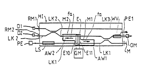
Fig. 5 shows a: integrated optical heterodyne interfero-
meter (:iI) . Arranged on the crystal (R) are three light-
guide channels (LKl, - LK3) connected together by selec-
tive ~:ode couplers. The device is fed by a pu:.ip wave (PE)
impinging on the laser (LS), wrich incorporates rare-earth
doping and the e.-.:itted light fra:;, ~ah:.ch supplies the
interferometer. Arranged on the crystal ara t=ao acoustic
waveguides (AW1, A~d2) ~ahich are fed via an electro-
acoustic tra, sducer (E) , t::e electrodes (E10, Ell) o'
which are fed from a modulation generator (GM). The
waveguides (A~~II, ATA2) for: :~odul ators (M1. M2) along with
the lig:~t-guide channels (L~l, LK2), said modulators
s::ifti: g the fr2yuer.cy of so:;.e cf t :e light waves by t'e
acous tic fr equ2ncy ( f a ) . The f it s t waveguid2 chaan 21
(LR1) is bounded by a .:.irror (M) , a:.d the second waveguid2
c::an:el (LK2) is bounded by a subject ~2flactor (OM) ~ahic::
.:,odulates the li7ht Taav2 by t::2 :~eas::rable variable. ':h2
r ef lected :ncdula t2d Taave is a..~..pl if ied '-n a ty av211 ir.g-wave
'" p' ' f i ( r ) ' ~. ~. p . . ~ . :, ~ , r
4... -~ 2. !~r L v. 'e Olt 3:. 'au~C.: w:12 TOSS S L Oi.I v...2
S'..:b j 8C t ar A C :..~.,p2~aSa.'~cG~ . .'~-rS G=2SC~ ~~2~ . t:l:.S tr
dV2~~:.:1C~'-
wale a.'.;pl' t' 2r (~~1V) i COrpOrateS a "'a"'e-2ar t~:-d0~2d rcgiOZ
~'C ~ahich pi::.~.p ligh t (PEZ) iS fed. At t :2 2ndS the two
lly::.i.-~l:~G~.c channel S ( LcZ2 , LIC3 ) i::CO~ y70rate d2 t2C tOrS (.'~. t
,
..n.G) , ~ArliC:1 Conv2r t t::2 2iler.J~, i.~.C~' O''ySt~.Ca1 SigIlalS i nt0
eleCtriCal Signals 'AhiCh are Sent t0 d differential
analyser in conventional manner. Te basic functions of
such a heterodyne i.~.ter f erome ter are ou tl;n2d in EP 90 IG 5
787.
One advantageous variant of the heterodyne inte=~a~ometer
is exposed to or.Iy one, suitably polarised pu:~p light wave
(PE), by allowing said wave at the ends through a
wavelength-sel2Ctive mirror (MR), from where it passes
along the light-guide channels (LR1, LFC2) to the
travell ing-~aave amplifier (WV) and supplies pump energy
thereto. The second pump entrance is then no longer
2101~~1
necessary. The pump light wave returning from the
travel'_iry-reeve a:.~.plifier (T~J) is reflected bac'r, into the
system at the exits ahead of the detectors (D1, D2)
through wavelength-se-ective mirrors (RM1, RM2) for
further use and kept remora from the detectors.
Fig . 6 schematically shows the ~anufactur ing process is
seven steps. In the first step of the process, a photo-
resist (PR) structured usi.~.g conventional technology is
applied to the su5strate, thereby producing a phetoresist-
Fr ee channel above the rare-ear th doping r egio n. In a
second step the rare earth is applied by spu,.,.eri ng or
vacuum-evaporaticn as a :petal or :petal cxida layer (SS) ,
after which t he phetorasist (P.°,) with the layer (SS)
thereon is detached usi:.7 the so-called lift-off
technique. This step therefo:e gives rise on the surface
r v f t ~y ~ a- .. ~ a..ich
,S, c a c_ star ,~) to a r '~e-ear t~ strip (SS1) r
:.:1 t h2 ne::t St2a.~. :..~. the pr.~.CcSS iS dl:.F::SZt1 i»t0 the
Crystal (~'.t) . "'a:~S .~.~ffLlSiO:a 15 C~r~~e..~. CL:t .~')~r f~rSt
.., r:.". r-v i ,- ., .. ..~. ..~ h te:~~= t::re and
t.....~W ~..y v.i :. a'.'. ni'~cn 3v..uvS~...a2~.., t a ..p....a
d;:ration being eel acted sc as t;, attai.. a preset di_fusion
depth that is Hess than the depth of the liyht-guide
c hen pal to be inserted subsequently. ~t ras bee : shcan
that in the case of a Z-suction of a lit :iu:,i niobat~
crystal a diffusion depth of about 5 r.;. is achieved in 100
hours at 1050°C, and at 1080°C a diffusion depth cf about
7.2 ;~~: is achieved. The diffusion dept h is dater:.i~ ned by
the 1/e concentration of the surface concentration.
T: further also known
a step
of
the
process
a
silica
gel,
as sol gel (SG), is applied to tile Crystal surface (S)
a
and the a sec.cnd temper ing opera tion (
n II ) car ried out ,
causing tile doping to diffuse Out close to the surface
intothe gal, an ,~'. thereby prod~,:cing a
doping centre (Z) of
maximum the crystal
ccncentr
ation
below
the
surf
ace
(
S
)
of
t~).~t tile same time the rare-earth doping region (SE)
_ - 2~.~~~~~.
12
penetrates deeper into the crystal (K). Ia a further step
a layer of titanium (Ti) is put onto the structured
photoresist (PR) and the surface (S) of the crystal (FC),
after 'which the phctoresist is lifted off along with the
titaniu:~., layer . The titanium (Ti) remaini ng on the
surface (S) is then diffused into the crystal (R) in a
third tempering step (III) in an argon/oxygen atmosphere.
The titaniu:,t strip (Ti) is at first situated above the
centre (Z) of the rare-earth doping, with the result that
subsequently the light-guide channel coincides in axially
parallel :.~.a nner with the previous doping (see Fig. 1) .
Ideally a layer initially 95 nm thick is used for the
tita n'_u.;, dopir:g, said layer being diffused for 10 hcurs at
1050°C. Such a waveguide is first and fore.;.ost suited
trazs.:.issicz ef a 1.53 ~::~ wavel engt::. It is also suited
to :aen:.:~ode cperat_cn.
7 S hOSdS anOth2r m2t::Od O~ lat.'-.r311y deli:~i.',.i:..J.'T tile
.. iy .
~C~ :. ys:y,... Channe . ihiS i.~OC SS 1. JO~VcS rS dyp~~~..~
t h2 r 3r ~-83i th layer (.~'$ ) OVer a lar "~J2 ar 2a Cn t::2 Cr ~.'i, vii
(1T.) a:.d di~~::Si:y i.'. in t:.e ~:.rSt tE':~iper~:lCJ Oper,:ti:.. (I) .
glar.ar optical waveguide is t:en produced over a lacy'
area usi :g tita ni',::.t diffuson cr a proton e:tchange
process.
I n a fur t her s tep a pt~.otoresis t is applied to the large-
area dopi :g region (SE) and so structured using the
convention al method that a photoresist strip (PR1) is lef t
over ~ahat will 1 ater be the light-guide cha nnel . In a
next step the surplus doped material to the side of the
photoresist is etched away using ion etching, after which
i : a next step t he photorasist is detached. This then
leaves a narrow strip waveguide doped 'with the rare earth
on the crystal (R).
214~.~4~.
13
Fib. 8 shows a doping cross-section as it appears a_'ter
the f it s t tesper ing step ( I ) and the dif fusion te:~per ing
step (I) . It transpires that the concentration (FtZ)
initially exhibits a half-bell-curvy distribution, and
following the second te:~pering stage (II) at a cer rain
depth below the surface (S) comprises a :,:axi:nu:.~. concen-
tration (ZS) that is higher t:~.an a surface concentration
(CS>. Doping extends to a 1/e doping depth (TS) that is
far greater thar. after the first te.:~pering step (~) .
In place of t~taniu~; diffusion, in tha exa:,ipl2s relati ng
to Figs. 1, 3, 5, 7 and 8 it is also possible to use a
proton a ;change process, preferably using a :netall'_c mask,
a . g . of Cr /Ti or Ta to d2f ine the wid th Cf t:~.e cha.~.n21.
benzoic aci : :,felt is left to act o : t::2 crystal for I
::curs at appro:t. 2C0°C, and t:zis is follo'aed by te:.~.rering
at 350°C for 3 to 4 hours. T::is :net'.~.od has tha advantage
t :at because cf t a lc'a te:;.p,2r atur 2s t here is r.C r eal
post-diffusion of tz2 rare-ear th dCri:.g.
S~13V27L:.G~2S rr:,duc2,a. in t:.is way have t~2 advantage cf
being free of optically-induced :efractive ir.d2:C c:~a:.gas;
hOW2'T2r , t::2y Cr.ly CCnVey t h2 '~TaV25 ir. t: 2 2xtr aOrCai:ld
ry
pClarisation. This efface is explo'_ta.~'. in laser or
tray=sling-wave amps ifi2r Q-co ntral, in that by ccr.trol-
lyng the pc~ar~siag rotation the active section is
attenuated to a greater cr lesser degree.
The titanium-diffused waveguides have the advantage that
they convey both types of polarisation, and this makes
th2:.~, par ticul ar ly suited to pol arisation-convertin g
processas. ~. dra'aback of the light-guide channels thus
produced is the fact that they are not entirely free of
optically-induced refractive index change. The
censa~uence of this is felt in particular for wavelengths
below one micrometer, which occur when neodyme is used as
210~.~~:~
t :2 :are-eartz doping material. Because the faavelength c:
the erbium emission is above ons micrometar, in the case
of erbium doping t his property of t!-.e :,~.aterial is nct a
critical one.
It is partic;~larly advantageous to use erbium as the
doping :..aterial because its emission wavelength of I. 53 u-:
fits the so-called third communication ~~i ndo~a of tha
fibr_-optic cables. This enables integrated oYtical
components, ~~rit:~ their advantages, to Se employed for
optical co:~:aunicatio n.
The Var ious r are-eart:~-doped componen is illus .r ated :.;ay be
p~ educed r ~' cr -,. , 1 , ."a ; ~ .. '; "T
s ny..y ..u t_p_y a.. ~Z any es_ 2,. ".;:bi na
c.~. a crystal substrata. T:~is res~,:lts in an in~.c.eassd
-t t~C n , '+. ~,~ ;..,...v'~y ;..C ; t '.".... mss. .-°
2gra ~ de s~:.y a .,. 5~...t.y _ 2c3 c-y u_ s, s~..,.~ ,...2_
are no int2r-:ediat2 1CSS2S 3t tzz ju.~.c tic n bat~~reen a
Yluralitj cf substrates a nd, fcr e:~a.-.:pl e, a pu.~.:p lig::t
sour ce is to .''.2 Su~Yli2'r to a plot ali ty of laser s and/or
r a Vc _:. -aa-re a... 1=f :, ~ ia,._
t 11~ g -~p '_2r s ~1 a~,~,r op~'' ~-~ dis tr ibution c.
.._. as Jas c.. ,...,.
~e ~ ° ~ "~ ~ subs tr a to . ?ho toll thograp~.ic tech: o logy
C3n s i::ul tar.2ous 1y .~~~.2 uS2d , ~ . 2 , ir. C n2 s t2i~. , ~Or ~.3C ~..
t::2
nOV21 CCi.lpCn2 ntS a nd fOr Cth2r , alt 2ady ~a.:.iliar
ntegr3t2d CptiCal CCmpOr.2nts prCdLlC2d C n tilt Sdi..2
5,,...Strate and advar.tagecusly abl a to be ccmbined ~aith the
novel ccmpo vents. This si:;pl~~i2s productior. ar.d
i ncreases the precisior. of the over all cir c~.~it .