Note: Descriptions are shown in the official language in which they were submitted.
LASER EXPOSURE APPARATUS FOR PRINTING FORMS
TO BE IMAGEWISE EXPOSE~
Backqround of the Invention
The present invention relates to a laser exposure
apparatus for printing forms or printing plates to be
imagewise exposed. More particularly, the present
invention relates to a laser exposure apparatus for
printing forms to be imagewise exposed and comprising a
laser, beam divider, modulator, beam expander, polygonal
ln mirror, scanner lens, reference mask and path-folding
mirror.
From DE-B 12 14 085 (U.S. Patent No. 3,144,331) it
is known to expose photopolymerizable recording materials
which have been applied as a photosensitive layer to a
printing plate support and whose sensitivity has fallen
due to absorption of molecular oxygen, using 70 to 98% of
the radiation dose of an actinic radiation which would be
necessary with uniform incidence to initiate a photopoly-
merization in order to restore the sensitivity. The
exposure is carried out through the printing plate
support, which is, for example, transparent, an actinic
radiation being used which has a wavelength such that
only 10 to 70% of the radiation is absorbed by the
photopolymerizable layer. In this process, exposure is
in principle carried out first diffusely and then image-
wise. The diffuse or preexposure is carried out with
lower intensity, namely with 70 to 98% of the radiation
intensity which is necessary to achieve the full exposure
action. This preexposure is then followed by the
imagewise exposure with full radiation intensity.
U.S. Patent No. 4,298,803 discloses a process in
which a photoresist layer is preexposed with an intensity
which is less than the critical exposure intensity at
which the photoresist can be substantially dissolved away
at the exposed points, After this preexposure, the
-2~ ~,~ J~
imagewise exposure of the photoresist layer is carried
out. The sequence of the two exposures can be
interchanged. In both cases, the photosensitivity of the
photoresist is improved, which considerably shortens the
processing time. In the device used for this process,
both the imagewise exposure and the preexposure or
afterexposure of the photoresist can be carried out by
means of an electron beam, or of a UV or X-ray source.
U.S. Patent No. 4,716,097 likewise discloses a
process in which a photopolymeric layer containing a
dyestuff is first diffusely and then imagewise exposed to
light having a wavelength above 400 nm and an intensity
of at least 1500 lumens/m2.
German Offenlegungsschrift DE-A 24 12 571 discloses
a process for curing a light-curable polymer layer of a
printing plate, in which exposure is first carried out
diffusely for a short time and then imagewise until the
polymer layer is virtually completely cured in the
exposed areas. The diffuse exposure duration is not more
than 90% of the time within which the complete curing of
the polymer layer takes place with equal intensity of
radiation both for the preexposure and for the imagewise
exposure.
Summary of the Invention
Accordingly, it is an object of the present invention
to provide a laser exposure apparatus for printing forms
to be imagewise exposed in such a way that the radiation
sensitivity of the photopolymerizable recording layer of
the printing form is increased and the information loss
can be kept low, in each case relative to the exposure in
a laser exposure apparatus having a laser as sole
exposure source.
In accomplishing these objects and others, there has
been provided according to one aspect of the present
invention a laser exposure apparatus having a laser light
-3 ~ U~ ~ 2
source for producing a beam of light together with means
for splitting the beam into separate writing and
reference beams. The writing beam passes through a
modulator and is then recombined with the reference beam.
A polygonal mirror and path-folding mirror further direct
the writing beam onto a printing form to produce an
imagewise exposure. The laser exposure apparatus is
further provided with at least one additional exposure
device. The additional exposure device is disposed in a
closed housing near an exposure slit through which the
laser beam of the laser strikes the printing form, and a
control system is provided for establishing a time
interval between an additional exposure and the main
exposure of between 1 second and 15 minutes.
In one preferred embodiment of the invention, the
additional exposure device is mounted upstream of the
exposure slit in the direction of movement of the
printing form through the laser exposure apparatus.
With this arranyement, a preexposure takes place
before the actual laser exposure of the printing form.
Equally, the invention can be embodied in such a way that
the additional exposure device is disposed downstream of
the exposure slit in the direction of movement of the
printing form through the laser exposure apparatus in
order to carry out an afterexposure of the laser-exposed
printing form. In a further development of the inven-
tion, an additional exposure device is present in each
case upstream and downstream of the exposure slit, and
only one of the additional exposure devices is switched
on in each case during the passage of a printing form
through the laser exposure apparatus.
Still another embodiment of the invention has been
provided in which a linear LED arrangement is employed as
an additional exposure device, and means for varying the
luminosity of the device are provided.
Additionally, there has been provided exposure of a
photosensitive printing form in an imagewise manner. A
linear portion of the printing form is first illuminated
-4- 2 ~- 9 ~ ~Ji~ 2
with a diffuse light source. A laser beam is produced
and split into a writing and a reference beam. The
writing beam is modulated in response to a synchronized
signal, expanded, and subsequently recombined with the
reference beam. The reference beam is directed onto a
reference mask containing a patterned glass plate, a
diffuser and a row of photodiodes. The synchronizing
signal is produced as a result of the output from the
photodiodes, and then used to control further modulation
of the writing beam. Finally, the modulated writing beam
is directed onto the preexposed portion of the printing
form after a delay of between one second and 15 minutes.
Further objects, features and advantages of the
present invention will become apparent from the detailed
description of preferred embodiments which follows, when
considered together with the attached figures of drawing.
Brief Description of the Drawinas
The inventlon is explained in greater detail below
by reference to the drawings, in which:
Figure 1 shows a diagrammatic perspective repre-
sentation of the main or laser exposure of a printing
form in a laser exposure apparatus according to the
invention;
Figure 2 shows a diagrammatic sectional view of a
laser exposure apparatus having additional exposure
devices for the preexposure or afterexposure of the
printing form; and
Figures 3 through 5 show a side view, plan view and
circuit schematic corresponding to the radiation source
of an additional exposure device according to the present
invention.
Detailed Description of Preferred Embodiments
The laser exposure apparatus according to the
invention is used to expose photopolymer-coated printing
_5- ~ 2
forms, in particular highly photosensitive laser plates,
in which process, as a result of the preexposure or
afterexposure with light of very low and very uniform
intensity, the photosensitivity of the printing forms
treated in this way can be increased appreciably. For
this purpose, the unexposed printing forms which are
exposed, for example after preexposure has been carried
out, by a laser having a wavelength of 488 nm or 514 nm,
are preexposed with very low intensity with the aid of
the additional exposure device to light of a wavelength
of A = 565 + 20 nm. An advantage of this additional
exposure device is that the luminosity of its radiation
source can be adjusted within very wide limits.
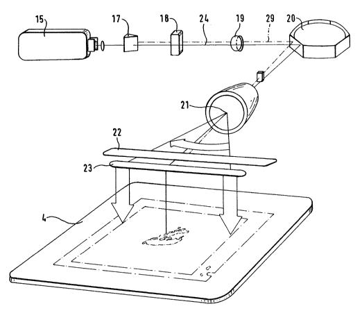
The elements, shown in a diagrammatic perspective
representation in Figure 1, for a laser exposure of a
printing form 4, for example a negative laser plate
Ozasol N90 supplied by HOECHST Aktiengesellschaft,
Frankfurt/Main, Germany, comprise a laser 15, a beam
divider 17, a modulator 18 for the reflected laser beam
or writing beam 24, a beam expander 19, a rotating
polygonal mirror 20 wh~ch the writing beam 24 and the
unreflected laser beam or reference beam 29 strike after
being brought together, a reference mask 22 and a path-
folding mirror 23 which guides the writing beam onto the
printing form 4. Such a laser exposure system is used
for the main exposure of a printing form 4 in a laser
exposure apparatus 1 such as that shown diagrammatically
in sectional view in Figure 2. The same elements as in
Figure 1 are provided with the same reference numerals in
Figure 2. The laser beam of the laser 15 is divided in
the beam divider 17 into the reflected laser beam or
writing beam 24 (shown in continuous lines), and into the
unreflected laser beam or reference beam 29, (shown by
dotted lines). The writing beam 24 passes through the
modulator 18 which allows through or blocks the writing
beam 24 in accordance with a control signal. The control
signal is supplied by a data memory in which the
information of the image to be reproduced is stored in
,.. ..
.
-6- 2 3 a ~
binary form. The writing beam 24 then passes through the
beam expander 19, comprising a system of two lenses which
can be moved towards one another to focus the writing
beam 24. Downstream of the beam expander 19, the writing
beam strikes a beam combiner 28 and is brought together
by the latter with the reference beam 29, which, after
passing through the beam divider 17, is guided onto the
beam combiner 28 by path-folding mirrors 26, 27. The
beam combiner 28 guides writing beam 24 and reference
beam 29 onto the polygonal mirror 20 which guides the
writing beam 24 over the width of the printing form 4 as
a result of its rotation. Downstream of the polygonal
mirror 20, the two beams 24, 29 pass through a scanner or
scanning lens 21 which ensures that arc-like curvature of
the beams 24, 29 due to the polygonal mirror is smoothed
out so that the beams travel on in a straight line after
passing through the scanning lens. Downstream of the
scanning lens 21, the writing beam 24 strikes the path-
folding mirror 23 which guides it vertically downwardly
through an exposure slit 13 onto the printing form 4
which passes through the laser exposure apparatus 1 in
the direction of arrow A and which is exposed by the
writing beam 24. The reference beam 29 strikes the
reference mask 22 which comprises a glass plate having a
broken-line pattern, diffuser plate and a row of diodes.
The diffuser plate evens out the radiation intensity of
the reference beam 29 that passes through the broken-line
pattern and strikes one of the diodes, which supplies an
appropriate synchronization signal to the modulator 18 in
3~ order to synchronize the opening and closing of the
latter, with the control signal being applied in each
case from the above-mentioned data memory.
Each of the additional exposure devices 2, 2' shown
diagrammatically in section in Figure 2 has a housing 14
which is closed off at the bottom by a plate, which is a
light scattering plate 6 mounted in a housing opening 5
of the underside of the housing. Printing forms 4, two
of which are diagrammatically shown in Figure 2, travel
_7_ ~ 2
along a conveyance track 16 in the direction of arrow A
past the additional exposure devices 2, 2' and underneath
tlhe latter. An electronic control 7 for a radiation
source in the form of a linear LED arrangement 8 is
accommodated in the housing 14. The luminosity of the
radiation source is measured by a sensor 3 which is
mounted on the radiation side of the linear LED
arrangement.
In Figure 2, two additional exposure devices 2, 2'
for the preexposure and afterexposure of the printing
form 4 are disposed on both sides of the exposure slit
13. Obviously, the laser exposure apparatus 1 may also
be equipped only with one of the two additional exposure
devices 2, 2', either one for the preexposure only or one
for the afterexposure only. As a result of the
preexposure, the photopolymerizable recording layer of
the printing form 4 becomes more photosensitive since it
begins to crosslink at a lower potential than in the case
of the main exposure. The information loss, in
particular in the case of narrow information ranges, the
so-called peak-point information, is kept low as a result
of the incipient crosslinking during the preexposure.
If an afterexposure is carried out as a second
exposure, the photosensitivity of the printing forms is
generally not increased as considerably as in the case of
preexposure. A possible explanation could be that the
crosslinking remains smaller compared with preexposure
since fewer free radicals are formed because the oxygen
concentration remains constant. However, it is the case
both for preexposure and for afterexposure that the
photosensitivity of the printing form 4 is increased,
when compared with the exclusive main exposure by a laser
beam.
Together with the light scattering plate, the linear
LED arrangement 8 provides for the full area diffuse
exposure of the printing form 4. This linear LED arran-
gement 8 comprises at least two rows, offset with respect
to one another, of LED modules D1, D2, ... Dn and D1, D2
-8~ 2 ~
... Dn~ as shown in Figures 4 and 5, and is situated in
a closed housing 14 of the additional exposure device 2.
At the bottom, in the direction of the conveyance track
16 for printing forms, the housing 14 has the exposure
opening 5 which is covered by the light scattering plate
6.
The single module D1, ... Dn~ D1 ... Dn generally
comprises four light-emitting diodes (LF.Ds) which are
connected in series, as shown in Figure 5. Two modules
D1, D1; D2, D2 -- Dn~ Dn are in each case connected in
series and are fed with a reference voltage Uref by a
current source, which is not shown. Two modules
connected in series are in each case controlled by an
electrical circuit comprising transistor T; and current-
limiting resistor Rj, where i = l, 2, ... n. Theresistor R; may be a fixed resistor or a variable
resistor in the form of a potentiometer. The current
source applies the reference voltage Uref to the bases of
all the transistors Tj, which are connected in parallel.
The resistors Rj, which are likewise connected in
parallel, limit the emitter currents of the transistors
T~. The reference voltage Uref is a direct voltage in the
range from about 0 to 3 V, in which case a base-emitter
current IBE of about 0 to 30 mA flows, or it is a square-
wave voltage in the range from about 0 to 6 V, with abase-emitter current IBE of about 0 to 60 mA, and a duty
cycle of about l:2. The current source of the reference
voltage Uref supplies a current in the order of magnitude
of about lO0 mA and may, for example, be a D/A converter
having a buffer stage, or a separate control circuit.
The effective luminosity of the linear LED
arrangement 8 is measured by the sensor 3. In order to
maintain a uniform illumination over the entire width of
the linear LED arrangement 8, LED modules from one
manufacturer are used. If differences in brightness
nevertheless occur between the individual modules, they
are equalized by altering the associated resistor Rj.
., ' '
:
9~ J~ ~
The LED modules Dl, D~ ~ ... Dnl Dn are disposed on
segments 11 which have equal or different lengths and are
plugged together by means of plug contacts 12 to form a
printed circuit board 9, as can be seen from Eigure 4.
A single module or two to four modules may be disposed on
the single segment 11. The plug contacts 12 are
indicated by dotted lines in Figure 4. One segment 11,
in each case having one module and two modules in the
upper row of the linear LED arrangement 8, is marked by
a curved bracket. The plugged-together printed circuit
board 9 is mounted on a base printed circuit board 10 on
which the transistors T; and resistors R; are also
disposed. Since the individual segments may have
different lengths, the row length can be matched to the
width of the printing form to be exposed. As a result of
the segmented structure of the linear LED arrangement 8,
a rapid replacement is possible in the event of a failure
of one or more LED modules since the functioning
components do not have to be demounted. No spectral
alteration, i.e. no displacement of the wavelength range
emitted, occurs with the ageing of the LED. AS a result
of the current control of the LED modules, a uniform
luminous power can be set over the entire length of the
linear LED arrangement 8, which is operated by low
voltage.
The illuminance of the linear LED arrangement 8 of
the additional exposure devices 2, 2' can be infinitely
varied electronically to precisely dose the amount of
light applied to the printing form 4 between 0% and 100%
of the maximum illuminance. The illuminance of said
linear LED arrangement 8 is indicated digitally, the
sensor 3 being mounted in the interior of the housing to
measure the illuminance. The closed nature of the
housing prevents the occurrence of external unwanted
radiation which could adversely affect the measurement of
the illuminance by means of the sensor 3 in an
undesirable way.
'' ' , ' ' " ' ~ ' .
: -
.~
' ~
', -
.
--10-- 2 ~ ~ ~ r ~? ~
The illuminance of the linear LED arrangement 8 is
set by the electronic control 7, which is shown
diagrammatically above the linear LED arrangement 8.
The spectral distribution of the linear LED
arrangement 8 is in the wavelength region of about 565
20 nm.
The sensor 3 for measuring the illuminance is
normally a photodiode which is situated in the housing 14
of the additional exposure device 2 and is thereby
screened from any unwanted radiation such as, for
example, daylight entering the housing 14. The
photodiode is expediently mounted above the printed
circuit board 9 (cf. Figure 3).
The additional exposure devices 2, 2' achieve the
advantages that the linear LED arrangement 8 generates a
very uniform exposure intensity over the working width of
the printing form 4, and the exposure intensity of the
LED modules or of the linear LED arrangement 8 can be
infinitely varied. The results of the exposure for
different exposure intensities are always reproducible.
An ageing of the LED module does not cause a spectral
displacement, with the result that the wavelength emitted
remains substantially constant. Further advantages of
the additional exposure devices 2, 2' are that no un-
wanted irradiation can occur in the region of the addi-
tional exposure devices, that the linear LED arrangement
8 can be configured as desired in its length and can be
utilized for exposure in its full length, and that it can
be operated with low voltage and can be adjusted in the
range from 0 to 100% of its luminous power.