Note: Descriptions are shown in the official language in which they were submitted.
:
'''' 2~0~sl~.a
:
A TRANSCONDUCTANCE AMPLIFIER CIRCUIT
FIELD OF THE INV~NTION
; The invention relates to a transconductance amplifier
circuit, i.e. a circuit that delivers an alternating output
current that reproduces an alternating input voltage in both
amplitude and phase.
: BACKGROUND OF THE INVENTION :~
Such transconductance amplifier circuits are known, and
have served the c~ ?rcial purpose of providing a controlled
current source, which may be required in a number of practical
applications, one example being the testing and calibration of
wattmeters.
The basic requirement of a transconductance amplifier in
precision measurements is that it faithfully reproduce the
input voltage waveform as a current. This result has
traditionally been achieved by measuring the output current
with a resistive shunt and using the shunt voltage drop as a
feedback signal to compare with the input. However, when a
j~ large output current is involved, it i~ difficult to construct
a shunt that will have sufficient magnitude stability and a
; sufficiently low phase angle error. The current comparator is
an instrument that has been used as a means to overcome this
problem, its very accurate ratio characteristics enabling a
high value resistor with small magnitude and phase errors to
be used as a reference.
PRIOR ART
One example of a combination of a current comparator with
a transconductance amplifier i5 provided in E. So's U.SO
Patent No. 4,795,969 issued January 3, 1989 (also published in
IEEE Transactions on Power Delivery, Vol. 3, No. 4, October
1988 under the title "A Current-Comparator-Based Load Loss
Standard for In-situ Calibration o~ Transformer Loss Measuring
Systems") This patent discloses coupling the output from a
2 ~ a~ 0
transconductance amplifier (through a two-stage current
transformer) to a current comparator to enable comparison of
such output with a current proportional to the input voltage
derived from a reference resistor. Any unbalanced ampere-
turns in the cw xent comparator are detected and used togenerate a feedback signal that is applied to the input of the
transconductance amplifier. ;~
A variation of this technique employing a feed-forward
correction signal is disclosed in P.N. Miljanic's U.S. Patent
No. 4,884,038 issued November 28, 1989. See also
P.N. Miljanic "Calibrator for Alternating Voltage, Current,
and Power", published in IEEE Transactions on In~L~ul.. cntation '
and Neasurement, Vol. 38, No. 2, April 1989; and P.N. Miljanic
et al. "High Precision Range Extenders for an AC Calibrator up '~
to 600 V and 100 A", published in IEEE Transactions on ~ ~'
Instrumentation and Measurement, Vol. 40, No. 2, April 1991.
~he feed-forward te~-hni que employs an unbalance signal from a
current c ~rator to direc~ly modify the ~uL~u~ of the
transconductance amplifier, rather than to achieve this result
indirectly by modifyiny the input to such amplifier. ;~
SUMMARY OF ~HE lN V ~ ON
In the prior feedbac~ circuits there could be stability
problems causing oscillation, depending upon the type of load
of the overall system. The prior feed-forward circuits lack
isolation of the output current, which is required when
feeding into a high voltage circuit.
The principal object of the present invention is to
overcome these problems.
Another object of the present invention is to provide a
circuit that, not only has improved stability of operation and
effective isolation of the output current, but can deliver
these improvements while opexating with high current outputs,
e.g. up to 1000 amps or greater.
For these purposes the invention builds on the basic
prior art assembly o~
~ ' 2 ~
(a) a transconductance amplifier for generating an
output current corresponding to an input voltage,
(b) a reference resistor also connected across the input
voltage for providing a reference current, and
(c) currerlt comparator means (a current comparator
preferably together with a two-stage current transformer or
other ratio extender) for comparing currents ~hat are
respectively proportional to the o~ u~ and reference currents
and for generating a feed-forward error signal proportional to
an unbalance between the compared currents. This error signal
(preferably subject to amplification) is then applied to the
output current.
The novel addition to this basic assembly provided by the
present invention, includes passing the output current through
an output transformer (current injecting transformer) that
comprises inner and outer co~ lly arranged toroidal magnetic
cores. This output transformer has a primary winding and a
correction win~;~g both extpn~;ng around the outer core so as
to couple eleeLL~ ~netically with both cores, and a detection
w;n~;n~ located between the cores that couples electro-
magnetically only with the inner core. The primary winding is
connected to receive the ouL~uL current from the trans-
conductance amplifier; the correction winding is connected to -
receive the feed-forward error signal; and the detection
w;n~;n~ is connected to inject back into the current
- comparator means a current that corresponds to the error of
the output transformer (its magnetizing current). The
secondary winding of this output transfo~mer preferably takes
the form of a single conductor extending through the hole
defined by the toroidal cores.
Other features of specific embodimen~s of the invention,
together with their performance and advantages, will be
described below in relation to the drawings.
~RIEF DESCRIPTION OF THE DRAWINGS
Figure 1 is a circuit diagram of a preferred embodiment
of the invention; and
. :. '
l ' 2 ~
t Figure 2 is a cut-away perspective view of an output
transformer used in this circuit.
DETAILED DESCRIPTION OF THE ~K~KKED EMBODIMENTS
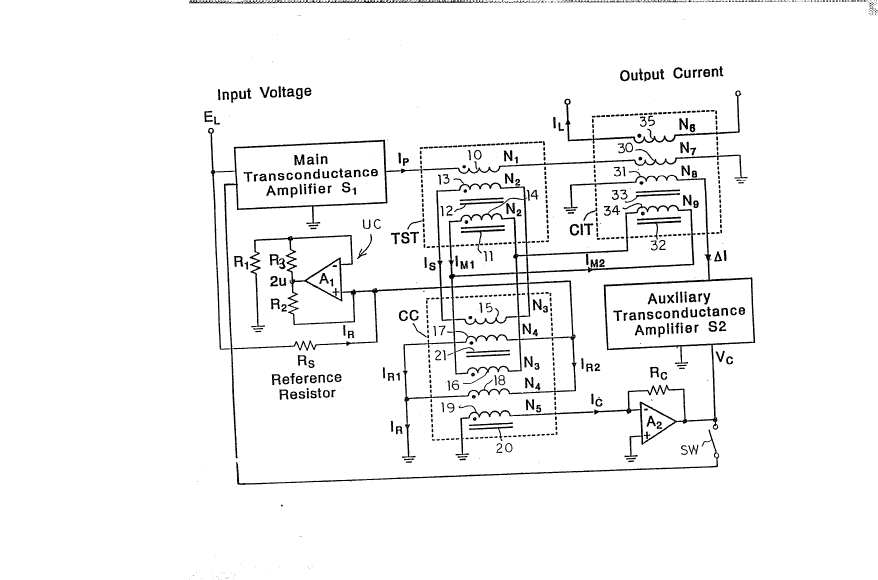
Figure 1 shows a main transconductance amplifier S~
connected to rec:eive an alternating input voltage E~. The
output current Ip from the amplifier S1 is passed first through
a primary winding 10 of a two-stage current transformer TST
and finally through a primary winding 30 of an ou~uL or so-
called current injecting transformer CIT.
The two-stage current transformer TST has inner and
outer, prefexably toroidal, cores 11 and 12, and two secondary ~
windings 13 and 14. All three windings 10, 13 and 14 couple '
electromagnetically with the inner core 11, while only the -
outer windings 10 and 14 couple electromagnetically with the -~
outer core 12. The secondary windings 13, 14 are respectively
connected across a ratio w; n~; n~ 15 and a compensation winding
16 of a current comparator CC. The current comparator Cc also
includes a ratio winding 17 and a compensating winding 18
connected in parallel with each other across the input voltage
EL through a reference resistor Rs that is chosen to be stable
and have a low phase defect. Finally, the current comparator
CC has a winding 19 for detecting any unbalance of ampere-
turns.
The current comparator CC has inner and outer toroidal
magnetic cores 20 and 21. A11 the w;nd;ngs 15 - 19 couple
electromagnetically with the inner core 20, while only the
outer w~n~;n~s 15 and 17 couple ele~LL~ ~gnetically with the
outer core 21. The two-stage current transformer TST itself,
the current comparator CC itself, and their combination are
all known, having been shown in Fig. 1 of the So patent
referred to above. The two~tage transformer TST acts as a
ratio extPn~er for the current comparator CC and could be
replaced by an electronically-aided current transformer; or it
could even be omitted entirely if the system were used with
only small currents. In this latter case, the output current ~'
Ip from the transconductance amplifier s1 would be passed ~;
" 2~0~
directly through a ratio winding of the current comparator.
With or without the ratio extending function of the current
transformer TST employed, one or both of the ratio and
compensation windings of the current comparator CC passes a
total measurement current proportional to the current Ip, and
hence a current that includes the error in the current Ip
arising from the imperfection of the main transconductance
amplifier S1.
An amplifier Al with resistors R1, R2 and R3 (the values of
Rl and R3 being the same) constitutes an unloading circuit UC,
i.e. a circuit that unloads the combined impedance o~ the
windings 17 and 18 from the circuit comprising the input
voltage EL and the reference resistor Rs~ thus maintaining the
total current IR through the windings 17, 18 independent of
such combined impedance. This unloading circuit is known ~er
se, and, although its use is pre~erred, it also can be omitted
if the combined imp~ncP of the windings 17, 18 is small or
negligible with respect to the resistance value o~ the
reference resistor Rs~
The detection winding 19 of the current comparator CC
provides a current I~ that represents an error feed-forward
~; signal to be applied ultimately to the output transformer CIT.
However, because the amplitude of the current Ic is small, it
is preferably amplified by a current to voltage amplifier A2
with an associated resistor Rc to produce a voltage Vc,
followed by a second or auxiIiary transconductance amplifier S2
to produce the final error current ~I from its input voltage
Vc. This current ~I is passed through a correction winding 31
of the ouL~uL transformer CIT.
! 30 The transformer CIT (seen physically in Figure 2) is
toroidal and has inner and outer cores 32 and 33, a correction
winding 31 outside the outer core 33, and a detection winding
34 between the cores. A secondary winding 35 is also shown in
the circuit of Figure 1, but only forms part of the trans-
former when it is connected to an external circuit that -
recei~es the uuL~uL current IL, since the function of the
secondary winding will normally be performed by a heavy
~$1 ~
;
conductor or busbar (not shown) extending through the hole 36
defined by the toroidal cores, thus constituting a single turn
secondary. Only the outer windings 30, 31 and 35 couple
electromagneticcally with the outer core 33, while all the
w;n~;ngs 30, 31, 32 and 35 couple electromagnetically with the
inner core 32.
The output from the detection winding 34, i.e. the
magnetizing current IM2 ~f the transformer CIT, is connected
across the c~ ~n~tion winding 16 of the current comparator
CC to be added to the magnetizing current IM1 ~f the current
transformer TST.
The numerals N1 to N9 in Figure 1 signify the number of
turns on the respective w; n~; ngs of the transformers TST and
CIT and the current comparator CC.
The current comparator CC provides a means for measuring
the combined errors caused by the magnitude and phase errors
of the main transconductance ampli~ier S1 and the magnetizing
error of the output transformer CIT. These combined errors
are measured indirectly, using the current comparator CC and
its ratio extender TST, by comparing the sum of the output
current Ip of the main transconductance amplifier S1 (reduced
proportionately by the two-stage current transformer TST) and
the magnetizing current IMZ ~f the o~L~uL transformer CIT, with
the reference current IR obtained by applying the input voltage
EL through the reference resistor Rs. The unbalanced ampere-
turns in the current comparator CC is therefore a measure of
these combined errors. The voltage Vc proportional to this
unbalance ampere-turns, derived from the detection winding 19
through the amplifier A2, is then used to drive the auxiliary
transconductance amplifier S2 to provide the feed-forward error
current ~I to the correction winding 31 of the output
transformer CIT, resulting in a highly accurate and stable ~
load current I~ in the secondary of such transformer. ~ ;
Neglecting the capacitive currents in the current-ratio ~;
devices and assuming negligible loading effect on the two-
stage current transformer TST, the following e~uations are
valid within an accuracy of a few parts per million (ppm)
.
2 1~
N1. IP -- N2 (IS + IM1) = ~ (1)
N7~ IP + N8' ~I ~ N6- IL ~ N9 IM2 ~ (2)
N4' (EL/RS) ~ N3' IS ~ N3' (IM1 ~ IM2) NS IC
E ~ G ( 4 )
~I = RC' IC GA
Equations (1), ( 2 ) and (3) show the ampere-turn balances
of the two-stage current transformer TST, the output
transformer CIT, and the current co~p~rator CC, respectively.
Equation (4) gives the ouL~u~ current of the main transcon-
ductance amplifier S1 as a function of its input voltage E~ andits transconductance GMI i.e. its output current divided by its
input voltage. Finally, equation (5) gives the error ~eed-
forward current ~I as a function of the feedback resistor Rc of
the amplifier A2, the transconductance GA of the auxiliary
transconductance amplifier S2, and the current Ic in the
detection w; n~; ng 19 of the current comparator CC.
If N1-N9 = Nz N7 (6)
GM = (l/RS) (N2/N1) (N~N3) (1 + eM) (7)
GA = (1/RC)- (N5/N3)- (N9/N8) (1 + eA) (8)
eM2 = (N9/N6) (IM2/IL)
where e~, eA, are the complex errors of the in-phase and
quadrature components of the main and auxiliary
transconductance amplifiers, respectively, and eH2 is the
complex error due to the magnetizing current of the output
25 transform~r CIT, then the following expression for the ou~put
load current IL can be derived
I - (N4/N3)-(N9/N6)-(EL/Rs)-(l + eA (eMz eM)) (10)
With this error feed-forward technique, the remaining '
errors are errors of an error and these are negligible.
Equation (10) therefore becomes
I~ = (N~N3)-(N9!N6) (EL/Rs) (11)
As a result, a highly accurate current will be
established in the single turn secondary of the output
transformer CIT which is thus an inductive coupling device
35 with the unique property that, without a galvanic connection,
the current established in the secondary conductor threaded
through the hole 36 i~ highly accurate to a few ppm. This ~-
~ ~,
2 ~
property i5 important, because it enables the overall
transconductance amplifier circuit to feed a highly accurate
output current to an external circuit that can be operated at
a high voltage that is isolated from the transconductance
amplifier circuit itself.
Nonlinearities in the main transconductance amplifier S
could cause distortion in the waveform of its output current
Ip. This, in turn, could cause a high harmonic content in the
unbalanced ampere-turns signal Vc. These harmonics could
saturate the amplifier A2 and/or the auxiliary transconductance
amplifier S2, causing a large error in the feed-forward error
signal ~I, thereby compromising the overall accuracy of the
output current IL~ To minimize this problem, and also the
effects o~ large drifts in the main transconductance amplifier
S1, a switch SW can be closed to establish a feedback of the
unbalanced ampere-turns signal Vc to ~he input o~ the main
transconductance amplifier Sl. Since only ;n;r~l loop gain in
this ~eedback is required, no instability problems causing
oscillation can arise.
Solely by way of specific examples not limiting the
invention, some of the values that can typically be used are
as follows.
The main transconductance amplifier Sl is a commercial ~ ;
transconductance amplifier of 3 kVA, its input being
redesigned to accept an input voltage of up to 100 V with
manual adjustment of both the magnitude and phase of the
output current up to 20 A. Thus the nominal transconductance
of the amplifier is GM = ~ . 2 S and its compliance voltage at
20 A is 150 V.
The output transformer CIT is designed for operation up
to 1000 ampere-turns with a 3 kVA burden. With a one-turn
secondary winding, it is capable of providing a load current I~
of up to 1000 A with an equivalent compliance voltage of 3 V.
I The magnetic cores of this output transformer are such that '~
3s one completely encloses the other in a toroidal shielding
arrangement. The primary w;n~;n~ 30 has 50 turns, being made
of five windings of 50 turns each connected in parallel. The
~ 21~8 ~
number of turns of the secondary winding 35 depends on how
many turns are threaded through the hole 36. For a single
turn secondary winding, to provide a load current of up to
1000 A, a copper bar insulated for high-voltage operation of
up to 50 kV is used. If more turns are required, for load
currents lower than 1000 A, then a high-voltage cable with a
suitable connector arrangement to obtain 1, 2, 3, 4, 6 or 12
turns can be used. The correction w;n~;n~ 31, driven from the
auxiliary transconductance amplifier S2 by the error feed-
forward current ~I, has only one turn. The detection winding34 has 1000 turns and is wound uniformly around the inner
magnetic core 32. The current IMZ in the detection winding 34
is proportional to the magnetizing error or the magnetizing
component of the current in the primary winding 30. As
already explained, this magnetizing error current is added to -
the error component of the ouL~uL current Ip of the main
transconductance amplifier, using the current comparator CC
with its ratio extender TST, to obtain the total combined
error. The combined error, proportional to the unbalanced
ampere-turns in the current comparator is then used to drive
the auxiliary transconductance amplifier S2, which in turn
provides the error feed-forward current ~I to the correction
i winding 31.
The auxiliary transconductance amplifier Sz is a
commercial transconductance amplifier of 20 VA with a nominal
transconductance ~f GA = 1 S and an accuracy of better than
1000 ppm at the power frequencies. This relatively small
amplifier provides an error cur~ent ~I up to 10 A rms. The
current ~I can be made as small as possible by minimizing the
output of the amplifier A2 which is the total combined error
deri~ed from the detection winding 19 of the current
comparator. This is achieved by manually adjusting the
magnitude and phase of the output current Ip of the main
transconductance amplifier S1 for a minimum output of the
amplifi~r A2. The current ~I consists of mainly higher
harmonic components, due to the distortion in the waveform of
the output current Ip of the main transconductance amplifier S
2 ~
caused by nonlinearities in the amplifier. An oscilloscope
can be used to monitor the output of the amplifier A2.
The ratio windings 15 and 17 (and their corresponding
compensation windings 16 and 18) have one turn and loo turns
respectively. q~he current c~ _ A rator has a n~ ;n~l current
rating of one ampere-turn. The reference current IR~ derived
from the input voltage through a 10 kn reference resistor R
is driven through the parallel connection of windings 17 and
18. Although the voltage across these windings is very small,
the unloading circuit UC is useful in reducing the quadrature
error of the reference current to the one ppm level. The
value of R~ is nominally equal to Rs~
The primary winding 10 o~ the two-stage current trans-
former TST is a 5-turn w;n~;n~ and the secondary w;n~ings 13
and 14 are 100-turn windings. To m;n; i~e the loading effect,
the first stage sPCon~ry winding 13 is connected to the ratio
w; n~; n~ 15 of the current comparator and the second stage
secondary winding 14 is connected to the corresponding
compensation winding 16 inside the magnetic shield 21. This
winding 16 is also used to introduce into the current
comparator CC the magnetizing current IU2 of the transformer
CIT. A 250-turn detection winding 19 is connected to the
current-to-voltage converter (amplifier A2) to obtain the -
voltage Vc proportional to, and in-phase with, the unbalanced
ampere-turns in the current comparator.
From equation (10), the stability and accuracy of the
load current I~ are det~r~; ne~ primarily by the basic ratio
accuracy of the current comparator CC, and the stability and
phase de~ect of the reference resistor Rs~ The combined errors
due to the errors of the main transconductance amplifier S~,
the auxiliary transconductance amplifier S~, and the output
transformer CIT are second order errors. The accuracy and
stability requirements of the two transconductance amplifiers
and those o~ the ~u~u~ trans~ormer are, therefore, not
critical. The error term eA (eH2 - eM) in equation (10) can be
made to be very small (less than one ppm), by adjusting the
complex error eH of the main transconductance amplifier S~ to
2 ~
be equal and opposite to the magnetizing error eM2 ~f the
transformer CIT. This can be achieved by adjusting the
magnitude and phase errors, using the manual adjustments of
the main transconductance amplifier S1, such that the output of
the amplifier A;, is zero or minimum, since such output is a
measure of the unbalanced ampere-turns in the current
comparator, which in turn is a measure of the combined error
(eM2 - eM). This condition may change due to instabilities in
the adjustments, and/or ~uL~L changes in the main transcon-
ductance amplifier S1 caused by nonlinearities or temperature ~ -
e~fects. However, the overall effect of the combined error ~; -
will still he negligible. For example, if the change due to a
drift in the amplifier is lO00 ppm and the error eA ~f the
; auxiliary transconductance amplifier S2 is lO00 ppm, then the
error term eA (eM2 - eM) is only l ppm. The ratio errors of the
current c~ p~rator including that of its ratio extender TST
are no greater than ~5 ppm in both magnitude and phase. The
stability and phase defect angle at the power frequencies of
the reference resistor Rs are +5 ppm and
+5 ~rad, respectively. The overall estimated uncertainties of
the load current I~ are therefore not more than +lO ppm in both
magnitude and phase (the root-sum-of-squares of the errors are
7 ppm for both magnitude and phase).
11