Note: Descriptions are shown in the official language in which they were submitted.
WO 93/19547 PCl'lUS93/00410
2~0~
P~se Adj~rtrnen~ M~1~hod and ~pparatus for IJ~e i~ a
ClocJ~ R~c~ Cir~
Field of the I..~e ~':o
T~is i~ ion :generally relates to clotik ~ecv~d~ r mPt~o~
and a~ Lu~l and more Q~er:r.~lly to a method and
1 0 ap~l,~ of phase ~ nent for u~e in a c~o~k ~ec~ ve
C;lO.u~ wi~ a .~iote~erhone CO~ QnR sy~tem.
Ba~grount ~of the Illv~-.L on
1~ 5 Recc ~tl, in t~ field of radio frequen~y (RF)
CO~ J~ nS~t there has been an iDc.~-~ed ~ nls~ntl for
~tPl~y~e"~ ed voice and high s~eed du~ o~ t;on~.
Since the~RF ~&cL~ is in~ limi~ one must devise a
new ~3L~ oo~c~pt and o~ ollal fe&l~e~ to
:; 2~0 ~ acco~odate~ the~:increased demand. A ~me di~sio~ m~ e
cces~ (TDMA~ ~s~ i8 o~e su~h 8~ h oiEers more
ffi~nt~8~ 7~ n and in~ l cupuci~y~
ptmpl~t form, aTDMA ~5l~ i8 c~ e~ of a
t~n~ base: ~tatic~,~ w~ is cPp~hle of time
2 ~5~ mllltiplexi~ m~rrlage~ ~om at least :two user~ o~ a siIlgle RF
h~nnP~ and one~or more remote ~W~viug Pt"~ hle of
,~c~iv~g~;~at~lea~t one oft;lle ~me Invltiple~stl messages.
:: Typicully,~ ~.v~g ,~tion would:be a mobile or partable
r~rliotP,lepho~e ~r~hl8 of t~n~ e a ~DMA mess~ge to
~: 3 ~ the buse ~t~1;Qq o~ a 8e~nd RF ~h~ el.
II1 a TD3~ ke mo8t ~ 1 c~ .7l-t.~J;c~tiQn,~
sy,~te~n~, ît is n?&~,g~P~ to e,~t~hliPl a .,~fei~ce ,~lock in the
::: . ec~ivillg ~;tot; )n 1;hat is r~ usly ~llc~ e,~ with the
~ ~ .
~:
WO g3~19547 PCI/US93/0~410
2I ~21 9 '~
nit cln~k ~ order to ac,~tely ~ec~.,r 1~he digital data
t~n~ lr~ we~ two rojnte Co~ it
chrQni7~t;on, a~ u~ed herein, means that the freqllency
and pha~e of the ~eeo;~rel cJock 8ignal must ac~.~dtely track
S that of t~e ~ ;t do~k.
Bit ~o~ cn over a mobile ~ cff~:~
channel c~n be .lifficl~lt to m~ ~;.., prima~ily due to
m~ ip~t~ fading. III ç l~i~;on to tracl~ng 1 he dri~ between t~e
m~il@ and ~e ~ta1;ion ç~ 8~ t~e clock .~uh"l ~, m~ch~ni~m
1 0 mu~t be 6~ffi~Pntly tolerant of noi~e ~u~ hat it does not
readily lose ~g~o-~;~ m ~ln~ing the penods of degraded
signal~ noise ratio caused by fi~ g. Hence, an ideal TDMA
mrb;le ~ock .ec-,.e ~ ~.,~1 would have fa~t init;~l aCq~ it;0n
of 6ymbol synchro~ ;Q~. and co~tinuougly m~ t~
~i 6yIl~o-)i7~;~ Wlth the base 8ite dock, e~en ~ ring peliod~
of ~ ig~l fir
One m~.d which has been devel~ to provide a
c o~ O~lPly ~ed c~o~k ~ for t;he mobile
radiote,~.r.pllone ~ a p~Fe I~L~ Ioop ~PLL) to recover a
2 0 ~ock i~l Ie9pOl~ 6 an ~ (Jr - :pt~e bit rate L:~..;..~ ~i~al
denved ~m l~he ,e~;v~l w~ve~o ~ .~t, how~vel-,
would have:~ifflclllty m~...t ;..;.~ ~chronization d~g
.e ~ of ~_~e fi~-li~ A ~econd te~ ue for ~lock recove~g
l-t;li7efi a: ~ ble di~ider coupled to a ~fe~ ock
: 2 5 ~ l. ~e reco.~e~l ~lo~ik signal i8 co~d to the ~aceived
~: : data eig~ d the di~nde ratio i~ mo~entalily altered to
8hif~c the phase of ~the rec~J~e~l caock. ~ in, thi~ phase
~Q~ ;S(~I le~ ue would generally lo~e synchroni7~q~isn
du~ing a perio~ of heavy r~
3 0 Further deve1o~ P have been made to ad~Les~ the
problem of 198~ng ~c~or~i~~t;Qn d-~rir ~ a ~e~re fade. One
such rne~o~l n~;1i7es ~ecei~e-l 8ig~1 ~ fs~ t;on
(RS~3I3 to de~e when the ~ce;vell sig~ oi~e ra~o is
wO 93/19547 Pcr/us93/00410
. 2~19~
poor due to a deep fade or signal dropout. When the RSSI fall~
below a predetemlined thre~hold, the dock ~.e.~ pha~e
E~ ;n~ is disabled, ~hereby~ random
pha~e adjustment of 1he ,~.e,ed ~lo~k signal. - -
S Althou8h thiB teCbl~iq~el offers improvet ~.fo.. --~Ice in
f~d~, it has ~e~e~ problems. Eirst, it ~ a~ an additional
;--tq, ~'~ce:to the ~lock ~.,Cv.."J ~ J for 1~e RSSI. .~eç~n~l,
additional c,~ i8 ,~d to p~BI~ 1 he RSSI. Third, t he
RSSI threshold need~ to be calib~ated for each radio due to
1 0 make tolerunces in the RSSI ~.,~1",. Finally, since this
t~c~ q~e uses ~ ed sig~al strength as a ~hannel quality
indicator, it ~nnot;detect poor ~nn~ quality csused by
strong ~nnel or adjacent ~el ~t4~e.c~lce. During
this 1ime t~e ,cco.e~el ~lo~k may ;jitter randomly and lose
l 5 syncLlu-~ *on;
.ef~,a, a~need e~i~t4 for a ~lo~ ec~ Wl~Uit which
will ,--Aj~ COllti~lU011~ 8~DChl'0 _on with t~e base
station tra~..uUing ~lo~k witb~ut the problem~ asso~qte~
:
with the.~a~.,e~entioned te~hnique~.
~: ::::
-:
~: .
:: : -
:: :~: :
.
~::
: :
WS~ 93~19547 . pcr/us93/oo41o
21~ 19~
of'Lho I~l~a~lion
The ~loBenl i~lve~-l on e~ es a method of phase
a~ G~ e,-l, for use in a ~locl~ r~ .e.~ s~heme. The phase
S a.lj~s~ent ~ auto~n~t;r~lly holds t~le clo~:k phase du~ng
rel:o-l~ of poor rhonrol quality, which oould be ç~oRe~l by such
co~ditions as mllltipath fading, signal Lo~ l, or ~trong
te~re~ence. ~e ~locJ~ r~.,v~el~ schem0 generates a ~mrliTlg
clocJ~ BigIlal which~ ous with the .~c~;ve.~
1 0 AAdit;c~~lly, the clo~ ,e. ~ s(~h~ e gen~. tee at least two
error Fign 1~ whi~ in l;~te the qualil y of She ~ec~;~,ed SigIl
at ~ ~ sampling phases. The ~lle~t error ~ignal is
~efe~el t~ as the "-;";-~ e~r ~ralue. Each error Pif~n~i is
cc....l r-.ed t~ t;he . ;~ - eDr ~alue, c,~ ~~ a
15 co~es~Q~.di~ llorm~u~~~ error ~n~ de ~ l Each
norm~ e~ error m~.;lv 1e signal i~ Ot'3BBC-l to dele~ e
the desired pha~e of the sampaing docl~ n~l DepçnAent
upon the ~oce~ ..g of t~ orm~li~ 1 error .. 9~ le
iFn~18, 1he h~e of ~he camp~g cl~ ~ i8 either ~hif ;e(l
: 2 0 o r m~;.. t ~ l t;he ~t ~ampling point.
: ::
:
~:
:~
:~:
WO 93~19547 PCr/US93/00410
2 1 ~
Brief l~esGr-rtion of $he D~a~
FM. 1 i8 a bloc~ .~ of the ~adiot~lepho~e
c~ *"-18 By~ acoordance ~vith the pre~ent
i~v~-.t:o~ .
FIG. 2 iB all eye diagram of ~/4 QPSK da~a at the oul~ut of a
~enL~ tect~r.
FIG. 3 is a block di~ of ~lock ~eco~ W~ l,y in
1 0 acco,da~ he ~.o~~t i~ lion.
FIG. 4 is a diagram ill~BL~l~; mn~ le phase offset
clocks used in t;he p~esellt ~ 1ion.
FIG. 5 i8 aD r~ e of a non-u~u~ mrli~ cJock
combining t~e ~di~iduaI ClOCkB of FIG. 4 in accordance with
1 5 t;he ~.~,~t ~. ../:~n
FM. 6 i~ a block di~,~ of lhe phase adjustment
~ ~ ~ o;~c.~ in accol~ance with l~e ~ ~ve.~l~o~
E'M. 7 is a ~ble def;~.;..~ the three level slicer ~how~ in the
~: : blo~ . of FIG. 6.
~20 ~FM.:8~is:glaph ~ eF,F~ ,1heclo~o.~
pe~r~ ce~ ~ollowing 8 ~c~ Lv~oul. in accordance
~: :vnththe presenti~ n.
E IG. 9 i8 a~ graph of 1 he a~bit e~r probabili~y verBus
signa~ noI~e ra~o in Rayleigh fi~ g for a col~vs~ ;on~l
25 system and:t~e~v~..Lion de~ hereiD.
;:
~:
:
WO 93/19547 PCl/US93/00410
f~ ~219'~
~ 6
Des~pt;ion of a I~f3..l.,.J. ~",~ .t ~t
The }~efel.ed em~ nt enco~ Ran~ a ~ig~ eceive
of a radiotelephone. lhe .~ trl ~ece;~s~r include~ ~e~tP;on-
S di.ecte.l ~lo~ik .¢cv.e. ~ ~c~l"~ for use in demo~ln~ he~ece;~¢.l oif~n l. The ~ ,r,~ tt eE amet~
of adjust~ the 8amplillg ph~e which provide~ inhere~t
p~ot~c~or ~in~t fadi~mdueed cloc~ mi~liEnmc~t~
Mu~a~Yef~ thi8 t~chniqil? i8 ea~ily implemented in either a
1 0 di~ J.or~or ~I)SP) or ~ logic ~c~ll-y. The
phase adj~L.Ierlt method j~ a nniq~l~ t;mit~
~ imin~nt w~ h has inherent fiade prot~c~;n~l; it
automalically hol~ i~ sa~ling pha~e ~11ri~e ~he fade
without the aid of a ~el quaLit~r indiu~to~ au~h as RSSI.
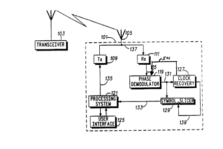
1 5 FIG. 1 i~ a block di6~ of a r~-UQt~lepholle dy~l~m
;: w~ich empl~ ~e y e~t i.. ~Lion. In t~e radiotelerhon~
y~tem, the fi~ed ~ 103 se~ d ~¢ceives radio
frequen~y (RF ) ~ignals to and f~om mobile and portable
r~ ot~-~.phoncs c4~ ed ~vi~n afi~ed ~,~o~ Lc area.
2 0 The r~dio t~leph~e 101 is one sush radiotel~phone ~e~ ~,t d by
t he fi~ed site tran~ 103.
While ~eco~Y~g n~l~ firom the fi~ed ~ite tr~nRceivel- 103,
:: the rr liot~vlephone 101 u~ e ~tc~ 10~ to couple the RF
signal a~d to comrert 1 he RF signal into ~ ele..~;c~l radio
2~5 ~ quency~i~ 137.: The ~ ~al iB ~eceived by
e radio~l~cc;ve~ 1iI for use ~ he ~ telephone 101.
The lece;~e~ 1l1 geDerateB a~ 7J~ le~equency (IF)
signal 116. Thi8 8ignal 115 ~8 ~put ~to t he phaBe ~nm~o~ tor
~i 119. The p~e demo~ln~ r 119 outputs a pha~e (lnmo~ ed
3 1) 8ig~ 131 for use by the clo~k ~e~.e,~ 127 and the
gmbo1 ~licer 129. I~e ~ C~ uh,r 127 out~puts the
center point c~ock 139 to ~e syn~ licer 129, The pha~e
demo~ t~r signal 131 i~ also used a~ eceived data ~ignal
:~
W~ 93/19547 PCI/US93/~0410
2 .L g. ~ r~
for 1~e 89mbol ~licer 129. The 8~bol ~licer in turn o~ uls a
~--Lol signal 133 for use by t~e proc~&~. 121. The ~ce~o,-
121 form~te 1 he 8~7mbO~ al 133 ~to voice and/or data for ~e
u~er i~te.~ce 12~ he wer ~te~ce 125 ~- ~t~;..~ a
. S microphone, a ppç~l~sr al}d a ke~
Upon L.~sion of RF ~ la fi~om thg porhble
rr~iot~ ~phorAe 101 to the ii~ed site tramloeiver 103,1~e voice
and/or data ~ om the user ~terfiEIce 12~ are proces~e~l
by the l~AbcQ~ 121. The AU~oc4Ap~ B are input into the
tr~n~ ;lll~ 109. The ~ a ~ el 109convert~ ~he pro&e~3se~
tO ele~ A~ ~al8~ The elecl;rical RF pi~n~l~
are I UAAVt;~ kd mto RF 8ignals ard ou~put by the ~ntenn~ 105.
The RF ~ A a~ ,.,.1 by the fi~ ite trPn~e.;v~r 103,
Wb~ A r~ to ~e l~nd li~ PhoAAe 8~
1 5 FIG. 2 is an illustration of ar eye disgram of a ~c/4
quadl~t~e p~e ~hiflc keying (QPSK~ sig~ at the Oul~ut of a
.lill[t A ~AA~aI ~ O t~; C t Q 1 . TbiB ~1 iB rep, ~ v e of the data
output o~ 1~e pbase de~ t~l ~ 131. For accurate
.e~ of ~e symbols 1~ te~ bet~veen the tr~nQceive.
2 0 :103 ~d t~e porl~blG _o~e 101, 1 he B~ J; ~ ~L C~OS1~ 139
should B~mpie 1~e occ;~l data ~ignal 131 at or near t~e
optimal 8~ rt as~ te~lAD FIG. 2. r E at
l'~ ..l~ other tha~ 1he ~I ~;mAl l~t;on ~ cause degraded bit
error rate (BER) ~ A
~: 2~ ; FIG. 3 is a de~ d bloc~ di~ m of ~ clo~ JV~
127 :t~ i7~d ~ the AJ~ emL4~ The ~oc~
e~ ~O~ use~ t~e pha~e dem~ tor oul~ut, signal
y(t) 131 to .ec~e. 1he c~o~k ~gn~l~ e p~efeA~e]
çmhodin~ent? the ~lock generation ~,~it 331 generate~ four
3 0 i~di~dual clo~k l~lgnalB 339~ 341/ 343~ 346. TheBe ~Ot~; a~e
used to ~mrle ar~Ad hold the pha~e d~ ~ c~ tor ou~u~ ~ignal
y(t) 131.
WO 93/19547 pcr/us93/oo41o
2:~2~ 8
Other e~lually suf~aient ~p~em~ntrti~o~s ~f ~he ~ ase~t
on may g~nerate tw~ or mors ~lo~k ei~ .r~
the pha~e aJj~l,..lents acco .li~ to 1he y,o~ent i~v~ n.
In the ~,~fe.,e~ em~in~ent~ the rela1;ive p~ eF of the
5 four clock ~ign~s are ~hown i~ EIG. 4. The on-time sigllal 405
ha~ a c~o~ pulse onoe ~ 8~ . ~al. The eat'ly clock
sig~al 407 ge~e.~,te~ a clo~k pulse at ~t~ .~ equal to the
~te~ .~la of the on-~ ~ 405, bu~ pba~e by V8 of
a symbol ~me before ~he on-time signal 405. The late clock
1 0 8igIlal 403 i6 equal in ~equen~ aDd ~ i~ by V8 of a ~ymbol
dl la~r ~1 he o~-tame signal 405. The half- B9m~)0
o~et clock ~ al 401 iB identical to the on-~me ~ignal in
f~equency aIld Pl~if~e~ b~ 1/2 a ~ymbol i~l~ 1. 01 her equally
~ert impl~tations may be used by ~ iug the phase
1 5 OrrAe~P but ~re B~ con~idered ~vithin the essence of the
i~ve~-l o~ disclosed herein.
The~e clocl~ are u~ed to sample ~e phs~e
demo~ rt~r ou~put dgnal 131 wi1 h the ~smple a~d hold
~i18 303~ 305~ 307r 30~. The~ sampled phases ~re the~
: 2 0 input into the ~:er ~ adder combi~atio~ to fo~m error
347, 3~9, 351, ~. The e~ror ~ignal iB ~ormed by t~kin~
~: : the di~,e~ce bet~ t~e ~ampled detector out~ut sig~ d
'che neareBt c~ pon~ de~P~ ~n point~ i.e., the ~licer
o~..l. :
2 5 . The e~r Pif~''lR 347, 349, 35l, 3~3, are ~put into l~e
8amp~ phasé adiustme~t c~.~l,~ 327. The ~mpl;n~
pha~e adjust~ent w.~ 327 i8 used to adva~lce or lalald t~e
: four s~hol ~ilo~ to ~ o the error at the on-~e
~mpline poi~t. 1~ ~he e~ror ~ ~dicate 'chat ~9 change in
3 0 t~e ~ Y~ E phase i~ en t~e s~mpti~ pha~e
:~ adjn~ t ~.,.~it 327 will ou~put o~e of ~e three rossib1e
clock adju~t~nPn~ eolnm~n~: "move earlyn, "move late", or
"move ~alf symbol". A move early co~ n~l will advance all
WO 93/19547 PCI'/US93~00410
2 1 ~
~our s~mbol ~lo~ 339, 341, 343, 34~ by V8 of a ~ol lime. A
move late command will r~ all ~our ~y~ol clocks by V8 of
a symbol ~me. ~~3imil~rly, the mo~re half ~_' Dl OOln~sm~ will
B~ift all four sy~ol ~locks by V2 of a s~l 1~ime. The cJock
gene~ation ~ il, 331 ~leo outputs an additional on-~;ime ~lock
~efe.red to ~ the ~amp~ ~ signal 139, which i~ used by
the s~mbol slicer 129 of FIG. 1.
Four i~ idual ~licers are shown in FIG. 3 for ea~e of
illustration. ~ equally sufficie~t ~m~lodiment may cQmhine
1 0 the ~y~ol ~licer 129 and t~e on-1ime s~ol ~licer 313, thereby
re~nring t;he ~ / ncco~J for clo~k ~ecvYe~
The non-~o ~ ~amp~ clo~k 501 of E IG. 5 is u~ed to
sample the p~ ~.ilLi~ the pha~e demu~nlP.tQr 119. It i~
formed by O~ 1 he four in~ lo~ 401, 403, 405, a~d
1 5 407.
Conventio~al ph~ue adju8tme~lt t~hnirlue~ Relect the
sampling phase wit~ 1~e e~ .e~t average error magnit~l~e as
~e~e~ ed di~ ~om~he error ~al8. During a deep
fade or sign~l Lo~oul ampli~g phase~ will yield p;mil~r
2 0 e~or ~ In respon~e, a co~ 1 p~e ad3~1Ft~n~nt
r~-h~ique wollld randon~ 8elect it~ Bamp~ g p~--e These
~:: rsln~lnm phase ~Q~ ;o~ would cause bit errQrs, los~ of
8~OII;7A~;;Qn~ and pot~-n~ 1y a dropped ct~ll.
In tbe~ .e.l e ~ ent, 1~e phase adju~ent
2 S w~ 327 ~ 6 its ~.e~ ~ l;,~ pha~e uIItil some
ot~er ~smpli~ e gield~ e~_ error m~ 4
W~l~h i8 e~?~fi~Pn~ly ~ all the o1~hers. Thi~ r~sults
in a ~ampli~g pba~ at will ~t ~ge in low ~ l to noise
ratio conditions. The i~ .o~,.l de~o~n ru~e~ for fis~mrlin~
3 0 pQ~t adjl~Rt~n~-nt ar~ im~l~ented m the blo~ diagram of
FIG. 6.
Ill the ~,efe~l em~i~nent, 1~he ~.,.~it ~ e~ to "move
- early", "move late", or "moYe half symbol". ~i8 pha~e
WO 93/19547 PCI/US93/00410
2 ~ 9 4
adju~tment teçhni~lue may al80 be applied to more
co.~e~LoIIal do~k ,cco~e. ~ loop~ w~ich per~nit only early alld
lat~ clocl~ adjl~Ft~n~te or sny other equally e~lffi~Qnt, clock
S FIG. 6 iB a block di~am i~ LdL;~g the i~vved phase
adjl~P~ ~ t t~chni~ e of 1~e preferred e~ ent. The fir~t
filn~ion of t~he sampli~g pha~e ad,jus1;ment ~l~t 327 i8 to
~iet~.Pnirle the m ~ of each error signal 347, 349, 351,
3B3, ~viL1~i~ 1 he bl~ 401, 403, 405, 407. Ne~t, t;he ~q11?rt
1 0 error m l~it~de ~ignal is ~ecte~l and caLled the .~
error value. T'ni~ error value i~ ~ubtracted fi~om
each of 1 he four error ~lalB 347, 349, 351, 3~;3, ~3~ ;r g in
four n~ e~: error ma~it~ ei~ ee l~rel
f~PiQ-~ iB then made for ea~h ~ampliIlg phase ae a fi~nction of
1 5 how its error -~;~ ~es to t;he ~ error
ms~nitude.
Table 700 of ~IG. 7 defines the logic ~ e~ e t~ree-
le~ er b10~ks 419, 421, 423, 425. If ~he e~ror ~r~ le
ffi~ P. .tJ.~ ~lose to t;he .. ~ value, or the
20 nC~ ti~e~l error m~ e i8 lee~ a t~res~old ~1. then
t;he C4 ~e~ g c~ e~ iB incremented. If 1~e error
m~nit~ large rela1;ive to 1 he ~-~ value, or t~e
no~rna1i7.etl e~or magnit~l~e is g~ te~ thaII a ~econ~l
- thre~h~ 2. t~en the co~ co~le- i~ decren~te~.
2 5 Pinally, if t~e ~or.n~i7ed e~r m~~ e f~ll8 wiL~ the
middle region, ~ he fir~t ~shold ~1. and lee~
than or eq:~l to t~e ~econd tL~e~ e~ the cou~ter is
held C~Q~nt ~
The fir~t of the four colln~r~ 433, 431, 429, 427, to reach a
3 0 pre~Qt~ ed l~o~live t hre~hold ha~ ted ~a~ its
e~or m~itude iB oQn~t~ntly e~AllP~r 1~haI~ 1~hat of ~e other
three s~m~ phases; hence, the ap~.o~;ate clo~
adju~t;ment ~e~ion i8 ~en made. ThiB i8 ca~Tied out iD the
wo 93/19547 PCr/uSg3/004l0
2:~21~4
11
block di~ by 1~ e output Yalue o~ 1 he C4j!~ ..te~ 6 input
into ~he CO1~)&~IO~D 435, 437, 439 441. HBre, th0 O~ Va1UeS
of the CQ~ ..te" ~ are compared to the predete~nin~A~ thre~hol~,
T. If one of ~e c~l~nt~ hes 1 he t~re~hold, ~hen al~ of the
cc~ Lb 433, 431, 429, 427 are re~et to zero, re~tar~g~he
ave~ ~occO~ for the p~e ad,juDtment w~,~l. The reset
fimc1;ion iB impleme~ted by ORiDg the outputs of the four
c(~ o~ the ~input OR gate 443, which iB then tied
to the re~et input~ of ea~h of 1 he four counters, 433, 431, 429,
1 0 427. The output of the fir.,t con~ or 435 îs equal to the move
early pbase adju~tmeIlt signal 355. The output of the ~ecol-d
comp~alo~ 437 iB not tied to a a~ 8~ ~ll~e the
desired p~ has alresdy been obtained. The ou~put of the
third co~ tor 439 is the signal 357 of ~IG. 3, w~ich i8 a
1 5 move late phase r~ Q!-~ nt Qi~ ~1, T'ne ou~put of t~le fourth
comparator 441 iB l~he move half ~mbol phase sdjl~ nt
l 359.
I~ 1 he ca~e of a deep fade or a si~al dropout, the four
error sigDals~ w;ll be random and ide~ically ~:~ihll~ l As a
2 0 ~ t, ea~ ~ffampling phase's error n~nit~ le will ~Yree~ the
:~: : ~ ~.. ;.... ~:valu:e more ofte~ 1~an it e~ ~e .. ;.. ;.. ~ value
by about a factor of 3 to 1 in ~ ~ f~l~d çmhoAim~~t,~ Thus~
with :th~ ~o~l ~ ~elec~io~ of the first thresh~ld level ~1 and the
second thre~ol 1 :level ~2 w.ithin ~IG. 7, all of ~he counters
2 5 will be decrem~te i ~ore often thaD ~ey are iI~crem~nte~l
Th~fore, none of 1 he co ~tY/ 8 Wil1 reaCh the ~Oa1l iVe
~: thre~hold, T, ~ e a time of ~ignal Lo~o~l or deep fade;
thUB, 1 he Bampling phaBe ~vill not change.
l~e fa~ e l~l r~~ r,s e of thiR phase adj~lPt~ent
3 0 techni~lue h~s been ~mnl~t~ 3 and compared to a more
C~VH~ n~1 early~la~e t~hnique ~1iRcllr~ pre~iously. To
enBure a~ ~lnh;~e~ A~ ~On, the two loop ~;~rs~~ol~ were
WO 93/1gS47 PCI/US93~00410
2 .~ ~J 2 ~ ~9 '~
12
nelecteA to yield iden'dc~ wlbng bandwidths equal to 0.001
. times t~e ~ymbol rate.
FIG. 8 plots ~he first performance te~t resultsc This test
e~m;~ed the l~ of 1ime the clock ~ could
S hold its ~amplin6 phalle duriDg a deep ~de. Thi~ was done by
ini~ g 1;he 8ampling phase to the co~sect value and then
remo~?ing the ~ignal ~o the loop would o~rP~ stric~ly on
thennal noise. The results plot the prob~bility of the clock
phase error ~ -ee~J;~ one qu~rter of a s~mbol Lime ~e~s the
l 0 time after the~ 8iglial dropout. The graph 8n1 ;11-J~t' ~teE the
conventioIlal;e~l~/late melhod and graph 803 illu~trates the
ofthepre~entL.~ on. A~there~ult~ te,the
prese~t ~lion holds its ulmpl ~g pha~ quite well,
whereas the co te~bnigue moves ~cantly off of
~: ~ 1 5 the co.. e~l;~mpli~g point a~er only 300 symbola. Thus, even
:though both 100~8 provide the ~ame tiacking capab~lity, the
clock sdju~tment:~,~t described herein does a eigr~ific~ntly
. job of mai~ t~i~ it'a ~lin6 pha~e throu~h the
duration of a:~de.:
2 0: ~ FIG. 9 i~ B ~a s~d perli~lmance evaluation. Thi8
evalualion plots~ bit error rate ver~us si~ t~ noise ratio for
42~1~1obit ~r aecond ~/4 QPSKmodul~ in 10 Hz Rayleigh
fadi~g. The~glaph:901re~ ~tp- the:conventionalearly~late
: terhn~ d the graph 903 ~epre~ 1 he ~ q~llt~ of the
2 5 ~ OE~t ,l~.~lion. Once:again. bol~:loops have identical
tra~g b~dwidths equal to 20 ~Iz. As 1 heae plots illu6trate,
e propo~ed.~ock:adj~ent c~.~t~provides near-
theoretical ~ ~. - -~ce, where~ the conventional ea~l~la~e
a~,oa~h 901 degrades filded bit e~Tor rate 1~. f~J~ -~ ce by
~: 3 0 about 1.5 dB at a ~*~b.it érror probability.
Described herein i8 a phase aJj~L..Ient ~.,~l for use in a
1 radiotelephone having ~lock ,e~.e,~ . This
invention offers a ~ienificant ~ fo~ ce ~p~u~.r~ .nt in
WO 93/19547 PCl /US93~00410
3 ~
~ing over previous designs ~ithout the addition~
and complications of U~iDg an e~ternal ~ignal quali1~r in~ic~tor
as ~e~l~ed by ~ome other conve~on~l t~rhn
What i8 claimed is:
; .
:
::
::