Note: Descriptions are shown in the official language in which they were submitted.
1
The present invention relates to optical fiber
communication systems, and more particularly to a
spontaneous emission source that is useful, for
example, in reducing non-linear effects in an
optical fiber used for communicating AM or other
information signals.
Optical transmission systems are currently being
implemented for use in various communication
applications. For example, telephone systems are
now in use that utilize optical fiber technology to
transmit voice and data signals over long distances.
Similarly, cable television network: are available
wherein optical fiber technology is used for the
transmission of both analog and digital signals.
In order to transmit an information signal
(e.g., a television signal) over an optical fiber, a
light beam ("carrier") must be modulated with the
information signal. The modulated carrier is then
2
transmitted to a receiver via the optical fiber. At
high power levels, silica fibers exYiibit non-linear
effects due to the interaction of the local electric
field across the fiber and the fibe~_~ material.
These non-linear effects also depend on the length
of the fiber, with a cumulative degradation of
performance resulting as the length of the fiber
increases.
Among the non-linear effects exhibited in silica
fibers at high power levels are four-wave mixing,
Brillouin gain, and Raman gain. The magnitude of
these interactions depend on the spectral density of
the applied field. The power of the optical signal
is also a factor in determining they severity of the
non-linear effects.
Very little effect on signal ti°ansmission is
seen below a threshold power density level.
Beginning at a critical power density level, power
will be shifted in wavelength by the non-linear
interaction between the traveling wave and the
material. Since optical fibers concentrate the
power into a small cross section, the large fields
required to make these effects significant arise at
modest absolute power levels. For long distance
signal transmission, these non-linear effects
constitute an upper limit on the power level that
can be transmitted. See, for example, Y. Aoki, K.
Tajima and I. Mito, "Input Power Limits of Single-
mode Optical Fiber Due to Simulated Brillouin
3
Scattering in Optical Communications Systems," IEEE
Journal of Licthtwave Technology, Mary 1988, pp. 710-
727 and Agrawal, Govind P., "Non-Linear Fiber
Optics", Academic Press 1989, ISBN 0-12-045140-9.
The non=linear effects in optical fibers are
particularly troublesome for the transmission of
amplitude modulated ("AM") signals, such as those
used in conventional analog television signal
broadcasting.
It would be advantageous to provide a method and
apparatus for reducing the non-lins~ar effects in
optical fiber for the transmission of information
signals, such as AM vestigial sideband (VSB-AM)
television signals at high power lEevels. The
present invention provides spontaneous emission
sources that are useful, for examp:Le, in broadening
the linewidth of lasers that output optical
carriers. Such carriers can be used to communicate
information signals via optical fiber links.
4
In accordance with the present invention,
spontaneous emission sources are provided for
reducing non-linear effects in an optical fiber used
for communicating information signals, such as AM
information signals, at high power levels. In the
common terminology used by those skilled in the art
of non-linear interactions, the terms "pump
wavelength" and "signal wavelength"' are used to
describe the stimulated Brillouin interaction.
Using this terminology, the signal laser in
accordance with certain embodiment:a of the present
invention plays the role of the pump laser. In such
cases, the classical signal laser .is absent since
there is no desire to use the Brillouin gain, which
gain would limit the achievable transmission
distance and increase the system relative intensity
noise from 0 Hz up to subcarriers a few times the
Brillouin bandwidth.
In the present invention, a laser output signal
is provided. The linewidth of the: laser output -
signal is increased to provide a broadened
optical signal. The optical signal is externally
modulated with an information signal (e.g., an AM
signal), and coupled to an optica_~ link fiber for
transmission to a receiver.
In order to increase the linewidth of a
longitudinal mode of a laser, a laser cavity is
5
provided for outputting an optical aignal having a
longitudinal mode. An active medium is pumped with
a pump laser to provide a source of excess
spontaneous emission at or near the lasing
wavelength of the laser cavity. The laser cavity is
pumped with the pump Laser while excess spontaneous
emission from the source thereof is injected into
the laser cavity to increase the li.newidth of said
mode. In an illustrated embodiment:, the laser
cavity is pumped by energy received from the pump
laser via the source of spontaneou~a emission.
A further embodiment of laser apparatus uses
spontaneous emission to provide an optical carrier
having a broad linewidth. A laser cavity outputs an
optical signal having a longitudin<~l mode. An
active medium having an output coupled to the laser
cavity is provided for injecting spontaneous
emission at or near the wavelength of said mode into
the cavity. A pump laser is provided to pump the
active medium for producing spontaneous emission
while simultaneously pumping the laser cavity to
produce the optical signal. In this manner, the
spontaneous emission in the laser cavity increases
the effective linewidth of said mode.
In an illustrated embodiment, the spontaneous
emission is injected into the lasEar cavity together
with the pumping energy for the laser cavity. The
active medium can comprise a Brat=~ng and a gain
medium coupled in series with the laser cavity, for
6
example, between the pump laser and the laser
cavity.
In yet another embodiment, laser apparatus for
providing an output signal with a broad linewidth
comprises a laser cavity for outputting an optical
signal to a first port of an optical circulator.
Spontaneous emission means, having an output coupled
to a second port of the optical circulator, injects
spontaneous emissions at or near th.e wavelength of a
longitudinal mode of the optical signal into the
laser cavity via the first port of the optical
circulator. A third port on the optical circulator
outputs the optical signal with the effective
linewidth of said mode increased by said spontaneous
emission. The laser cavity can be contained in a
ring laser having a first end coupled to~a first
port and a second end coupled to said third port of
the optical circulator. Such apparatus further
comprises an optical coupler coupled to the ring
laser for outputting the optical signal with the
increased effective linewidth.
Another embodiment of the present invention uses
a semiconductor laser to output an optical signal.
An optical amplifier is coupled in series with an
output of the laser for amplifying the optical
signal. The amplifier includes means for generating
spontaneous emissions at or near the wavelength of a
longitudinal mode of the optical signal. The
amplifier injects the spontaneous emissions into the
7
laser output. The spontaneous emissions injected
into the laser increase the effective linewidth of
said mode. Optical filter means can be coupled in
series between the laser and the optical amplifier,
for selecting at least one property of the
spontaneous emissions that are injected into the
laser output. For example, the filter means can
select the magnitude and spectral properties of the
spontaneous emissions.
. Another embodiment of the presESnt invention uses
a microchip or solid state laser for providing an
output signal with a broad linewidith. The laser is
responsive to pump energy for outputting an optical
signal. Means are provided for generating
spontaneous emissions at or near t:he wavelength of a
longitudinal mode of said optical signal. The
spontaneous emissions output from the generating
means are combined with the pump energy for input to
the microchip laser. The spontaneous emissions
input to the laser serve to increase the effective
linewidth of said mode.
A spontaneous emission source having a high
spectral density at a desired wavs:length is also
provided. The source comprises a guided wave
optical path that includes a grating and an active
medium. Optical energy is passed across said
grating and active medium within i~he optical path.
The optical energy excites the acitive medium without
lasing to output spontaneous emissions from the
8
optical path at a wavelength established by the
grating. The grating can reside in the active
medium portion of the optical path. In a preferred
embodiment, the active medium comprises a rare earth
doped portion of the optical fiber. The guided wave
optical path is formed either in a semiconductor
substrate or in a silica substrate. In an
embodiment where the guided wave optical path is
formed in a silica substrate, a planar waveguide can
be provided.
~~~.~!~~4
9
Figure 1 is a block diagram illustrating
apparatus in accordance with a first embodiment of
the present invention that uses broadband noise to
increase linewidth;
Figure 2 is a block diagram illustrating
apparatus in accordance with a second embodiment of
the present invention that uses a periodic function
input to an external modulator to increase
linewidth;
Figure 3 is a block diagram of a third
embodiment of the present invention wherein a
periodic function directly modulatsas a laser to
increase linewidth;
Figure 4 is a block diagram il:Lustrating
apparatus in accordance with a fourth embodiment of
the present invention that uses a espontaneous
emission source in series with a laser cavity to
increase linewidth;
Figure 5 is a block diagram illustrating
apparatus in accordance with a fifth embodiment of
the present invention that couples a spontaneous
emission source to a laser cavity via an optical
circulator;
Figure 6 is a block diagram illustrating
apparatus in accordance with a si~ah embodiment of
the present invention that uses an optical
~t~~Q~~~
circulator to couple a spontaneous emission source
to a ring laser to increase linewidth;
Figure 7 is a block diagram illustrating
apparatus in accordance with a seventh embodiment of
5 the present invention utilizing a different type of
ring laser;
Figure 8 is a block diagram illustrating
apparatus in accordance with an eighth embodiment of
the present invention that uses an optical amplifier
10 to inject spontaneous emissions into a semiconductor
laser to increase linewidth;
Figure 9 is a block diagram il:Lustrating
apparatus in accordance with a ninith embodiment of
the present invention wherein spontaneous emissions
are input to a microchip laser to increase
linewidth;
Figure 10 is a perspective view of a spontaneous
emission source formed from a semiconductor
substrate in accordance with the present invention;
and
Figure 11 is a perspective view of a spontaneous
emission source formed from a silica substrate in
accordance with. the present invention.
11
In accordance with the present: invention,
spontaneous emission sources are provided for use in
reducing the non-linear effects exhibited in an
optical fiber at high power levels due to the
spectral density of the optical signal. The
nonlinear effects are reduced to a level enabling
the transmission of AM communication signals at
relatively high power levels.
Currently, a high power solid state or
semiconductor laser for use in communications will
produce a signal on the order of 30 milliwatts or
so. The output powers of such lasers are increasing
at a rapid pace, and output power's on the order of
four watts or so are expected to become commercial
in the future. It is expected that even higher
power lasers will be available for communication
purposes in the not too distant future.
High power optical communication systems are
advantageous in that a signal can be split into a
plurality of paths (e. g., in a ti~ee and branch
distribution network). In addition, high power
enables the signals to be transmitted over longer
distances without the need for signal amplification.
This reduces the cost of the communication system.
Non-linear effects such as four-'wave mixing and
Brillouin gain have hampered efforts to provide a
cost effective high power optical communication
~1 p~r~~.~
' 12
system for AM signals, such as television signals
transmitted over a cable television network. In
order to overcome the non-linear effects for
relatively high power AM signals communicated over
an optical fiber, the present invention increases
the effective linewidth of the carrier light source
(e. g., laser) to reduce the effects. of fiber non-
linearity. Broadening the optical linewidth reduces
the spectral density of the signal, distributing the
same power over a broader range.
As an example, the Brillouin gain threshold is
reduced by the ratio ~vB/(~vH+Avp) where ~vp is the
optical linewidth (i.e., the linew:Ldth of the
optical field that induces the non--linearity) and
Llvg is the gain bandwidth of the Brillouin gain.
For typical single mode fibers, ~,vB is
approximately equal to 100 MHz. For a modulated
distributed feedback ("DFB") laser, the effective
~vp is on the order of 10 GHz and up. When a CW
laser and an external modulator serve as the pump
laser, ~vp can be as small as a fe:w kilohertz
depending on the specific source laser. Thus, a
wide range of Avp can exist, depending on the type
of laser used.
In practical vestigial sideband AM systems that
use external modulators, approximately 95% of the
optical power is concentrated within ~vp at vo,
13
where vo is the optical frequency of the non-linear
pump. For a typical single mode fiber having a
Brillouin gain bandwidth of about 100 MHz, a laser
providing a linewidth of two kHz will produce a gain
AvB/ (QvB+Qvp) ~1 . For a DFB laser having a
linewidth of six GHz, the Brillouin gain
QvB/ (QvH+Qvp) =.016 . Thus, we see t:he Brillouin
gain is much higher for the laser which has a two
kHz linewidth.
Optical broadening can be achisaved by an optical
angle modulator (e. g., frequency or phase
modulation) driven by broadband elE=_ctrical noise
(e.g., white noise having a 100 MH;a to 300 MHz
bandwidth) or a periodic function (e. g., sine wave)
to effectively increase the optical linewidth of a
light source. Injection of excess spontaneous
emissions into a laser cavity can also be used to
broaden the optical linewidth of an output signal.
As illustrated in the embodiment shown in Figure 1,
continuous wave laser l0 produces an optical
spectrum 12 having an optical frequency vo. The
narrow linewidth of the laser output signal is
increased by modulating it with broadband electrical
noise input to an optical modulator 14 at terminal
16. The resultant spectrum 18 output from optical
modulator 14 has a substantially increased linewidth
Qv. This optical signal, still centered around
~,~ Qf r~~
14
optical frequency vo, serves as an optical carrier
for communication of an information signal to a
conventional receiver 26 over a link fiber 24.
In order to modulate the optical carrier with
the information signal, an external. modulator 20 is
provided. This modulator can comprise, for example,
an electrooptic device such as a Mach Zehnder
modulator. External optical modulators are well
known in the art. See, e.g., S. E.. Miller, T. Li,
and E. A. J. Marcatili, "Research '.Coward Optical
Fiber Transmission Systems", Proc. IEEE, Vol. 61,
pp. 34-35, Dec. 1973. In the embodiment illustrated
in the figure, an RF AM signal, such as an AM VSB
television signal, is input to external modulator 20
via coaxial cable input terminal 22. The AM
modulated optical carrier is then received by
receiver 26 via the link fiber.
Optical modulator 14 can comprise either a phase
modulator or a frequency modulator. The linewidth
of the signal output from modulator 14 is selected
by controlling the bandwidth of the electrical noise
source and/or the optical modulation index of the
optical modulator. Optical phase modulators that
can be used in connection with thE~ present invention
are commercially available. For Eaxample, the Model
PM 315 modulator sold by Crystal Technology of Palo
Alto, California and the Model IOC 1000 modulator
sold by BT&D of Wilmington, Delaware.
15
A difficulty in realizing a pure optical phase
modulator such as modulator 14 illustrated in the
embodiment of Figure 1, is that if there are any
reflections the phase modulator aci:.s as a Fabry
Perot interferometer, which introduces unwanted
amplitude noise, i.e., relative intensity noise
(RIN). It has been recently reported that a lithium
niobate modulator can achieve virtually ideal phase
modulation. S. K. Korotky, et al., "High-Speed Low
Power Optical Modulator with Adjustable Chirp
Parameter," Integrated Photonics Research
Conference, Paper TuG2, April 9-11, 1991, Monterey,
California. Such a modulator can be used to
increase linewidth using a broadbamd electrical
noise source as illustrated in Figure 1.
Alternatively, such a modulator can be used to
increase linewidth using a sine wave as illustrated
in the embodiment of Figure 2.
As illustrated in Figure 2, a continuous wave
laser 30 provides an optical output signal having a
longitudinal mode 31 that is modulated in a phase
modulator 32 by a periodic function such as a sine
wave provided by source 34. By modulating this mode
with a sine wave in phase modulator 32, the
effective linewidth of mode 31 is increased as
illustrated by dotted line 33, to extend between the
first sideband components of the sinusoidal
modulation. Thus, if the periodlic function input
to phase modulator 32 is a sine wave, the effective
16
linewidth of the mode 31 will be broadened. Those
skilled in the art will appreciate that the actual
width of mode 31 remains narrow, but its effective
linewidth is increased by the frequency dithering
caused by the sinusoidal modulation.
The output 33 of phase modulator 32 is coupled
to an external modulator 36 that is the same as
modulator 20 described in connection with Figure 1.
An information signal input to the external
modulator modulates the optical signal for
transmission of the information via link fiber 40 to
a receiver 42.
Figure 3 illustrates another embodiment wherein
a distributed feedback (DFB) laser 50 is directly
modulated with a periodic function, such as a sine
wave provided by source 52. The modulation of the
DFB laser broadens the optical linewidth and reduces
the source coherence. For providing an optical
carrier for cable television applications, an RF
sine wave can be used to directly modulate DFB laser
50. The output of the laser will comprise an
optical signal having a longitudinal mode that
sweeps back and forth with the sine wave modulation.
In other words, the original longitudinal mode of
the laser is dithered between bounds established by
the frequency of the input periodic function. The
effect is that the average linewidth is widened,
providing a broadened output sign<~l to reduce the
system Brillouin threshold allowing higher power
~'~~ p'?
17
operation. The added advantage of.reduced
coherence length serves to reduce the susceptibility
of the system to beat noise degradation. Beat noise
degradation is the interferometric .conversion of
optical phase noise to intensity noise. In a
directly modulated DFB laser, beat noise degradation
is. manifest in the system as an increase in system
relative intensity noise (RIN). In a standard
externally modulated VSB-AM system, beat noise
degradation is seen as an increase in the phase
noise of the RF carriers.
The embodiment of Figure 3 illustrates optional
optical amplifiers 54 and 60, which can be provided
at the input and output ends, respectively, of
external modulator 56. As in the embodiments
illustrated in Figures 1 and 2, mo<iulator 56 can
comprise a Mach Zehnder type modulator to which an
information signal is input via coaxial cable
terminal 58. The information is carried via link
fiber 62 to a receiver 64 in a conventional manner.
It is also possible to increase the linewidth of
a longitudinal mode by injecting excess spontaneous
emission into a laser cavity. Various
implementations of such a system a.re illustrated in
Figures 4 through 9. Examples of spontaneous
emission sources implemented on semiconductor and
silica substrates are shown in Figures 10 and 11,
respectively. The spontaneous emission sources of
any of Figures 4 through 9 can be replaced with
18
either of the sources illustrated in Figures 10 and
11.
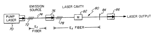
Figure 4 illustrates a linear embodiment wherein
an erbium fiber laser linewidth is .increased via the
injection of excess spontaneous emission into the
laser cavity. An active fiber 74 between a grating
72 and an optical isolator 76 generates excess
spontaneous emission at or near the laying
wavelength provided by a laser cavity generally
designated 80. The laying wavelength is determined
by grating 78 within the laser cavity. Active fiber
74 does not lase since .isolator 76 provides a very
low back reflection. Thus, the erbium fiber
extending from grating 72 to isolator 76 provides a
spontaneous emission source, when pumped by a pump
laser 70, for injection of spontaneous emission into
laser cavity 80 via isolator 76. Cfnabsorbed pump
power from pump laser 70 also propagates through
isolator 76 to excite laser cavity 80. The
unabsorbed pump power pumps the erbium fiber laser
defined by grating 78 and reflector 84. Although
such a design would be most efficiEant for delivering
spontaneous emissions at wavelengths that differ
from the laying wavelength, spontaneous emissions at
or near the laying wavelength (i.e., the wavelength
defined by grating 78) can be provided if grating 78
is chosen to have a reflectivity that passes a
relatively large amount of the spontaneous emission
from the emission source. For example, such a
CA 02102644 2001-05-16
19
result can be achieved if the reflectivity of
grating 78 is on the order of 50% at the lasing
wavelength. Mode selection within the laser
cavity is provided by conventional means 82,
such as the provision of a narrow Fabry Perot
within the laser cavity. Specific techniques
for mode selection are disclosed in commonly
assigned U.S. Patent No. 5,151,908, issued
on September 19,1992. After mode selection,
the light from laser cavity 80 is
passed through an optical isolator 86 for
output to an external modulator for the
information signal.
In the embodiment of Figure 5, an optical
circulator 100 is used to couple spontaneous
emissions into the laser cavity. Unlike the
embodiment of Figure 4, wherein the same pump laser
was used for both the spontaneous emission source
and the laser cavity, separate pump lasers are
provided in the embodiment of Figure 5. Pump laser
90 is used to excite a fiber laser generally
designated 94. A grating 92 is used to set the
lasing wavelength, and conventional mode selection
components 96 select a desired longitudinal mode.
The laser cavity extends between grating 92 and a
reflector 98, the output of which is coupled to a
first input port 102 of optical circulator 100.
A second pump laser 110 excites an active fiber
generally designated ?14. A grating 112 selects the
20
wavelength of the spontaneous emis~;ion. The
spontaneous emissions are input to a second port 104
of optical circulator 100. The spontaneous
emissions are coupled via circulator 100 to first
port 102, where they are fed back into laser cavity
94 via reflector 98, which passes t:he spontaneous
emission wavelength. The resultant: broadened
optical signal is .output via port 106 of optical
circulator 100, to an optical isolator 108. The
optical circulator provides an efficient method for
coupling spontaneous emission into the laser cavity.
Figure 6 illustrates an embodiment of the
present inventian wherein a ring cavity generally
designated 140 is used for the laser. Pump laser
120 is provided to excite the laser cavity. The
pump energy is coupled to the ring cavity via a
wavelength division multiplexes 122. An active
laser medium, for example an erbium doped fiber 141,
extends between wavelength division multiplexes 122
and a mode selector 124. A spontaneous emission
source generally designated 142 comprises a length
of erbium fiber having a grating 144 for
establishing the wavelength of the spontaneous
emission. Pump laser 148 is provided to pump the
erbium fiber to produce the spontaneous emission.
The output of the spontaneous emission generator is
coupled to an optical circulator 126 via port 130.
The spontaneous emission is injected into the laser
cavity 140 via port 128 of the optical circulator.
21
The resultant laser output signal .enters optical
circulator 126 via port 128, and outputs the
circulator via port 132. An optical coupler 134 is
used to output the laser signal via an optical
isolator 138. An optical isolator 136 is provided
within the laser ring cavity in a conventional
manner.
Another ring laser configuration is illustrated
in Figure 7. In this embodiment, pump laser 150
pumps the laser cavity 156. Mode selection is
provided by conventional components 154. An optical
circulator 158 receives spontaneous emissions from
source 168 via port 162. The spontaneous emission
source includes a pump laser 172, grating 170, and
active medium such as an erbium doped fiber 167.
Laser cavity 156 includes an active medium such as
erbium fiber 155 between the mode selector 154 and
optical circulator 158. The optical signal
generated by the laser cavity is input to port 160
of circulator 158 for output via port 164, optical
coupler 152, and optical isolator 166.
Spontaneous emission can also be used to broaden
the linewidth of a semiconductor :Laser signal.
Figure 8 illustrates an embodimeni~ in accordance
with the present invention, wherein spontaneous
emission from an optical amplifier 184 is injected
into a semiconductor laser 180. In a preferred
embodiment, an optional optical filter 182 can be
provided to select the magnitude and spectral
~~ t~~ ~4~
22
property of the spontaneous emission fed back into
the laser. The injection of spontaneous emission
into laser 180 causes a line broadening as described
above. The optical signal produced by the laser is
output via an optical isolator 186.,
Solid state or microchip lasers utilizing rare
earth laser systems can also be usead in accordance
with the present invention. An example of such a
system is illustrated in Figure 9. An erbium
microchip laser 196 is co-doped wiith erbium
ytterbium (Yb3+) to facilitate pumping by pump laser
190 at 1.06 ~.m. The pumping energ,~ is coupled to
the microchip laser 196 via a lens 194 in a
conventional manner. A spontaneous emission source
generally designated 206 includes .a pump laser 202,
grating 204, and an active medium 205 such as a
length of erbium fiber. As in the other
embodiments, grating 204 establishes the wavelength
of the spontaneous emissions. The spontaneous
emissions are coupled to the input of the microchip
laser via a wavelength division multiplexes 192.
The wavelength of the microchip laser is
controlled by a coating on the chip and the pump
laser spot size, in a well known manner. For
example, the input surface 195 of the laser can have
a coating with high reflectivity at 1.5 ~,m and a
high transmission at 1.06 ~.m. In this example, the
coating on the output side 197 of the laser would
have a high reflectivity at 1.06 ~Cm and a low
23
reflectivity at 1.5 Vim. The broadEaned mode from
laser 196 is output via a lens 198,, optical fiber
199, and optical isolator 200.
Figure 10 illustrates a spontaneous emission
source that can be used in accordance with any of
Figures 4 through 9 to generate the spontaneous
emission necessary to broaden the .Laser output. In
this embodiment, an integrated optical approach is
used, in which the emission source 210 comprises a
semiconductor substrate 212 having a guided wave
portion 214 provided therein. A grating 216 in the
guided wave portion establishes the wavelength of
the spontaneous emissions.
Substrate 212 can comprise, fo:r example, a
lithium niobate substrate. Local doping, defined,
e.g., by photolithography, is used to form the
integrated optical waveguide. The waveguide can be
formed from a rare earth material, such as erbium.
Ion implantation or indiffusion ca:n be used to dope
a surface layer of substrate 212 with the rare earth
material, thereby forming a doped integrated guided
wave optical path.
Figure 11 illustrates an alternative embodiment
of a spontaneous emission source i:n which an
integrated guided wave optical path 226 is formed in
a silica cladding 224 of a silica substrate 222.
Waveguide 226 of spontaneous emission source 220 is
doped with an active medium, such .as a rare earth
element. A grating 228 is provided within the
,.,.
24
optical path formed by the waveguid.e to establish a
wavelength at which spontaneous emissions will be
output from the waveguide. The waveguide containing
the active medium is pumped at a first end 230,
causing spontaneous emission to be output from
second end 232. Any conventional pump source, such
as a laser, can be used to pump the: device. It is
noted that other substrates, such ais polymers which
can be provided, e.g., as polymer films, can be
substituted for the silica substrate 222 and/or
cladding 224.
Planar waveguides such as those illustrated in
Figures 10 and 11 can be fabricated using well known
techniques. Examples of such techniques are
provided in P. Becker, et al, "Erbium-Doped
Integrated Optical Amplifiers and Lasers in Lithium
Niobate," Optical Amplifiers and Their Applications,
1992 Technical Digest Series, Vol. 17, pp. ThB4-4,
June 24-26, 1992, Santa Fe, New Mexico (integrated
optical waveguide and semiconductor. substrate) and
T. Kitagawa, et al, "Amplification in Erbium-Doped
Silica-Based Planar Lightwave Circuits," Optical
Am~~lifiers and Their Applications, Postdeadline
Papers, PD1, pp. 1-4, June 24-26, _L992, Sante Fe,
New Mexico (waveguides fabricated on silica
substrates by flame hydrolysis deposition and
reactive ion etching).
All of the laser embodiments illustrated in the
figures provide output signals with wide optical
25
line widths. These signals can be advantageously
used as optical carriers in communication systems,
by modulating the signals with an information signal
using an external modulator, such as a Mach Zehnder
modulator. The wide linewidth sources of the
present invention are applicable to any modulation
format which suffers from Brillouin gain. It should
be appreciated that although erbium laser systems
are used in the illustrated embodiments, the
inventive concepts may be applied i~o other laser
systems, including but not limited to neodymium
systems. The broadened optical signals provided in
accordance with the present invention reduce the
Brillouin threshold of the communication systems,
allowing higher launched power and therefore a
greater optical link budget. This advantage is
particularly useful in communication systems for
cable television applications, using VSB-AM signals.
It should now be appreciated that the present
invention provides apparatus and m<athods for
reducing the non-linear effects in link fiber by
increasing the optical linewidth o:E the signal
laser. In one illustrated embodim~ant, the optical
linewidth is increased by modulating the laser
output with broadband~electrical noise using an
optical modulator. This spreads the linewidth to
reduce the effects of fiber non-linearities. Such
non-linearities may include four-wave mixing,
Brillouin gain and Raman gain. Other illustrated
l
26
embodiments utilize a periodic funcaion, such as a
sine wave to externally or directly modulate a laser
to increase linewidth, or the injecaion of
spontaneous emission into the laser cavity to
achieve a broadened optical signa7L. Various
modulation formats will benefit from the broadened
linewidth sources, including VSB-AM, FM, PM, and
digital systems. The method and apparatus of the
present invention are effective for reducing any
fiber non-linear effect that depends on the optical
spectral density of the pump laser. As a result,
higher launch power can be accommodated.
Although the invention has been described in
connection with a particular embod:iment,~ those
skilled in the art will appreciate that numerous
modifications and adaptations may lbe made thereto
without departing from the spirit .and scope of the
invention as set forth in the claims.