Note: Descriptions are shown in the official language in which they were submitted.
PYROMETER TEMPERATURE MEA8U~EMEN~ OF PL~RAL
WAFERS 8TAC}~ED IN A PROCESSING C~ANBE~
Field of the Invention:
The present invention relates to the temperature
measurement of thin flat articles such as semiconductor
wafers, and particularly, to the measurement of the
temperature of pluralities of such articles stacked in racks
in processing chambers such as those of semiconductor wafer
processing machines. More particularly, the present
in~ention relates to pyrometer temperature measurement
techniques useful during batch thermal processes such as
those performed in semiconductor wafer processing machines,
for example, in batch preheating or degassing modules of a
semiconductor wafer processing cluster tools.
"~
WO92/21147 ` ~ PCT/US92/04066
sackcround of the Invention:
Semiconductor wafers are subjected to a
variety of processing steps in the course of the
manufacture of semiconductor devices. The
processing steps are usually carried out in sealed
vacuum chambers of wafer processing machines. Most
of the processes performed on the wafers require
the monitoring and control of the temperature of
the wafers during processing, and certain of these
- lO processes, such as degassing and annealing
- processes, have the heat treating of the wafers as
their essential process step. In several of such
- processes, particularly the essentially thermal
treatment processes, a plurality of wafers may be
stacked in a rack within a cham~er of the
processing machine and simultaneously processed as
a batch.
A variety of temperature sensing
techniques are employed in the various
- 20 semiconductor wafer treating processes to monitor
the temperature of the wafers and often also to
control the wafer heating or cooling elements.
Thermocouple devices, for example, are frequently
employed, particularly when a wafer is being
treated while held in thermal contact with a
temperature controlled wafer support. In such
cases, the thermocouple is often maintained in
21027~ S
WO92~21147 PCT/US92~04066
-- 3
contact with the support, and thus only indirectly
measures the temperature of the wafer on the
support. In certain other situation~, thermocouple
devices, are brought in direct contact with the
wafer. Such posi~ioning of the thermocouples may
expose the sensors to heat directly from the wafer
heating source, such as where radiant energy is
used to heat the wafer, or may, by direct contact
with the wafer, contribute to undesirable wafer
contamination.
Techniques have also been proposed for
deriving wafer temperature indirectly by measuring
the thermal expansion of the wafer. Such
techniques present a disadvantage in that such
measurements yield a reading proportional to
temperature difference. Accordingly, initial wafer
temperature must be known and a wafer dimension
must first be measured at the known initial
temperature before the monitored temperature can be
derived. Furthermore, such techniques can be
effective to read the temperature of a single
wafer, but these techniques are difficult to apply
where a plurality of wafers, particularly closely
spaced wafers, are processed and the temperature of
the wafer batch must be read.
In many wafer processing machines,
pyrometers are employed to measure the temperature
21027~' ` .
WO92/21147 PCT/US92/~ ~6
of wafers being processed within. These pyrometers
measure the emissive power of heated objects such
as the wafers. This emissive power, however,
varies with the emissivity of the object, which,
for some materials, varies`with temperature. The
emissivity particularly varies with the materials
of which the object is made and of the coatings
which have been applied to the object. In
semiconductor wafer processing, there are many
kinds of coatings that may be found on the wafers.
These coatings vary with the processes used on the
wafer. Accordingly, for a pyrometer to be used
accurately to measure the temperature of such a
coated wafer, an initial measurement to determine
lS the emissivity of the object is frequently
required.
As a result of the problems with
pyrometers, a number of schemes to measure wafer
temperature in semiconductor wafer processes have
been devised that either measure the emissivity of
the object or apply some sort of a correction to
the pyrometer output. Often a pyrometric
temperature is measured of an object of known
emissivity mounted in the chamber and known to be
at the same temperature as the wafer being
measured. Often also, a measurement is made with a
reference pyrometric sensor to generatè data that
21027~
W092~21147 PCT/US92/~
- 5
is then used to correct the temperature reading
from a primary parametric sensor to account for the
emissivity of the wafer being measured.
Measurement of wafer temperature from the ;
backside of a wafer may reduce the effect of the ~.
emissivity changes due to the coatings on the front
side of the wafer, but an initial problem is
encountered in that the uniformity of the backside
of the wafer is not precisely controlled, and may
vary from wafer to wafer.
Accordingly, there remains a problem of
accurately measuring the temperature of
semiconductor wafers or similar thin flat articles
during processing in semiconductor wafer processing :
lS machines. Particularly, there is a need for
measuring, without contact with the wafer, the
temperature of wafers, particularly where they are
being thermally processed in batches and may be
closely spaced in a stack within the processing
chamber.
Summarv of the Invention
It is a primar~ objective of the present
invention to provide an accurate noncontact
measurement of the temperature of thin flat
articles, such as semiconductor wafers, in a
processing chamber of a processing apparatus, and
particularly to measure the temperature of such
~ 1 0 2 ~ 9 ~
WO92r21147 PCT/US92/~066
-- 6
articles during processin~ in a batch and with the
articles arranged in a stack.
It is a particular objective of the
present invention to provide a pyrometer
temperature measurement technique that will
accurately measure the temperature of semiconductor
wafers in a chamber of a semiconductor wafer
processing apparatus, and that will measure the
temperature accurately independent of the
emissivity of the wafers or the coatings thereon.
According to the principles of the present
invention, a pyrometer is provided to measure the
emitted thermal radiation from a stack of articles,
particularly semiconductor wafers, being processed
in a chamber of a processing apparatus, by viewing
the articles from the side of the stack at an angle
to their surfaces. In the preferred em~odiment of
the invention, a directional pyrometer is inclined
toward the backsides of the wafers in a stack, so
that one or a plurality of the wafers located in a
central portion of the stack are viewed by the
pyrometer. Thermal energy received by the
pyrometer is restricted to the centrally located
wafers by ~he directional characteristics of the
pyrometer, which has a limited field-of-view around
the axis or line-of-site of the pyrometer.
2ln~s~
WO92/21147 PCT/US92/04~ :
- 7 - ;:
In the preferred embodiment of the present
invention, the pyrometer is provided outside a
processing chamber of a wafer processing apparatus,
such as a batch preheating degas module of a
semiconductor wafer processing cluster tool, in -
which the plurality of wafers are arranged in a
stack for batch pretreatment. The pyrometer is
aimed through a window in the wall of the
processing chamber, either in a direct linear path ~:
or in one directed by mirrors, at the side of the
stack of wafers. The wafers are usually circular,
and their circular edges define a surface of a
cylinder, which may be considered a boundary of
disc-like spaces between the parallel wafers. The
pyrometer is responsive to thermal energy of some --
wavelength, usually in the infrared band, and the
window is made of a material, such as barium
fluoride, that transmits energy of this wavelength.
` ~, In accordance with this preferred ~:
20~ : embodiment, the pyrometer is inclined at an angle
which is sufficient, with respect to the wafers of
a given diameter and spacing, to ensure that the
energy that is not directly emitted from or
transmitted through the wafers, but is incident
upon the pyromèter, will have encountered a
plurality of reflections, preferably at least eight
(8) reflections, from the opposed facing surfaces
y ~
WO92/21147 PCT/US92/~ ~6 -`
-- 8 --
of, and along the space between, the parallel
spaced wafers of the batch. Where there are highly
reflective coatings on one side of the wafer, the
number of reflections is preferably at least
fourteen (14), and with reflective coatings on both
sides of the wafers, the number of reflections is
preferably at least twenty (20).
In addition, the wafers viewed by the
pyrometer are preferably removed by at least one
wafer from the ends of the stack, and with highly
transmissive wafers, by several wafers from the
ends of the stack, so that equal amounts of energy
are transmitted in both directions through the
wafers adjacent to spaces that are within the field
of view of the pyrometer. With the wafers viewed
by the pyrometer being one or preferably more
wafers removed from the end wafer of the stack,
the energy transmitted through the wafer, if any,
is approximately equal to and cancelled by the
energy transmitted through the wafer from the
opposite side, since that transmitted energy
originates from another wafer of the same
temperature. As a result, the power received by
the pyrometer approximates that radiated from black
body that is at the sàme temperature as the wafers.
The pyrometer of the device of the present
invention is preferably configured to view from the
2 1. O ~ 7 9 ~
~092/21147 PCT/US92/~
_ 9 _
side of the stack and the backsides of the wafers,
for example, from the bottom of upwardly facing
wafers of a stack. Thus, the backsides~ of one or
more wafers and the spaces therebetween are in the
view of the pyrometer. The angle of the pyrometer
to the planes of the wafers of the stack is equal
to or greater than the minimum angle required to
ensure that a large number of reflections from
parallel wafer surfaces will be encountered by
light reflected through the stack to the pyrometer
at any angle within its field of view. This angle
is a function of geometric parameters that include
the diameter and spacing of the wafers. The larger
the diameter of the wafers and the closer the
lS spacing of the wafers, the shallower the angle may
be. It is important that the angle not be so
shallow that energy may pass on a straight line
from the chamber or chamber wall on the opposite
side of the wafer, or pass with too few
reflections, say two (~) or four (4) reflections,
before it enters th- pyrometer. -
The maximum angle of the direction of the
pyrometer toward the backside surfaces of the
wafers should also not be too great, or the
shadowing of one wafer by the edge of another and
reflections from wafer edges, which may not be -
perfectly aligned in the stack, may confuse the
2~ 02795
WO92/21147 PCT/VS92~04~6
-- 10 --
pyrometer reading. Ideally, the field-of-view of
the pyrometer would be small so that a minimum
pereentage of wafer edge, is in the field-of-view. .
Accordingly, embodied in a degas chamber
S of a semiconductor wafer processing cluster tool,
in which a plurality of wafers, 150 or 200 or more
millimeters in diameter, 0.75 millimeters in
thickness, approximately 2S in number arranged in a
stack and spaced approximately 9 millimeters apart,
the preferred angle of direction of a pyrometer is
about 40, for a pyrometer with a 7 or less field
of view. '
With the present invention, it has been
found that, with the angle of a pyrometer aimed at
the boundaries of the spaces between the center
three wafers of a stack of five or more parallel '~.
wafers in a degas processing chamber of a wafer
processing apparatus, the energy received by the
pyrometer exceeds approximately 98% of that
received from a black body.
With bare silicon wafers, the emissivit,y
of the wafers is approximately 0.4. With such
wafers, and with the net transmissivity of these
centrally positioned wafers being zero, the
reflectivity is 60%, and the energy received will
be even closer to that of a black body. The higher
the reflectivity of the wafer or its coatings, the :
greater the number of reflections required to achieve the
same approximation to black body characteristics. This can
be achieved with a steeper angle at which the pyrometer is
aimed at the stack.
The above described and other objectives and
advantages of the present invention will be more readily
apparent from the following detailed description of the ~-~
drawings in which:
Brief De~cription of the Drawings:
Fig~ 1 is a side elevational diagram, partially cut
away, of a portion of a degas module of a silicon wafter
processing cluster tool apparatus embodying principles of
the present invention.
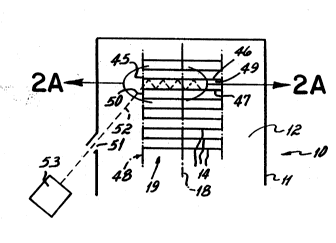
Fig. 2 is an enlarge diagrammatic view of the
encircled area 2-2 of Fig. 1.
F ~. 3 is a top view of a portion of the diagram of
Fig. 1. -
~ ~ ~'','`'
Detaile~ D-~cription of the Drawinq~:
Referring to Fig. 1, one embodiment of the present
20 invention is illustrated in a semiconductor wafer batch -
preheating nodule 10 of a semiconductor wafer processing ~-
aluster tool, such as that disclosed in commonly assigned
U.S. Patent No. 5,257,881, entitled "Wafer Processing
j--s
- 12 -
Cluster Tool Batch Preheating and Degassing Method and
Apparatus". The module 10 includes a sealed housing 11
enclosing a vacuum chamber 12 in which wafers 14 are
processed. In the illustrated embodiment of the module 10,
S the process performed is one of preheating or
preconditioning the wafers 14 for the purpose of removing
absorbed gases and vapors prior to the processing of the
wafers in other modules of the semiconductor wafer
processing apparatus.
In the module lO, the wafers 14 are supported in a
multiple wafer support or rack on which they are vertically
stacked. The wafers 14 are typically circular, thin flat
plates or planar disks of approximately 0.7s millimetres in
thickness and 150 millimetres, 200 millimetres or more in
diameter. When stacked on the rack, each of the wafers 14
lies in a horizontal plane and is spaced from and aligned
with the adjacent wafers on the stack 19 on a vertical axis
18.
The rack is supported in the chamber 12 on a
vertically movable and rotatable elevator. The rack has a
plurality of wafer holders formed by a plurality of slots in
four vertical quartz rods. The wafers 14 are individually
loaded into the rack as the elevator is vertically indexed
to bring each of the slots successively into alignment with
a wafer loading port in the housing 12. The port sealably
. , ", .
.. .. . ... . .. . , .. ..... ~ . . .. .. . ... ... .. . . . . ..
- 13 -
communicates between the vacuum chamber 12 inside of the
housing 11 and the interior vacuum chamber of a wafer
transport module, which has supported in it a robotic wafer
handling mechanism (not shown) for transferring wafers to
and from the degassing chamber 12 of the module 10 and to
and from other processing modules of the wafer processing
apparatus. The vacuum in the chamber 12 is maintained by
conventional cryogenic vacuum pumps connected to the chamber
12 through the housing ll.
In a typical heat treatment process such as the
batch preheating process performed with the module 10,
wafers 14 are individually loaded through the open gate
valve and into the slots or holders of the rack as the
elevator is indexed past the port. Then, the gate valve is
closed with the vacuuming chamber 12 at the same pressure
level as that in the chamber of the transport module.
In the preheating or degassing process, the pressure
in the chamber 12 may be changed to a pressure different
from that of the transport module or maintained at the same
pressure through operation of the pump assembly. In the
process, the wafers 14, which are stacked on the rack in the
sealed chamber 12, are uniformly brought to an elevated
temperature by the energizing of radiant heaters having
lamps arranged in sets on the outside of the chamber 12,
behind quartz windows in opposed walls of the housing 11.
This elevated or processing temperature, which may be, for
example, 500C, is usually maintained for some predetermined
processing time of, for example, fifteen minutes, during
which time the temperature must be monitored and controlled.
Accordingly to the preferred embodiment of the
present invention, at the front of the housing 11 there is
provided a vie~ port or window 51 positioned slightly above
the lower portion of the rack when the elevator is in the
elevated or processing position. The view port 51 is
preferably inclined upwardly at an angle ~, preferably equal
to of approximately 40, to the horizontal, as is better
illustrated by referring to Fig. 2 in conjunction with the
reference to Fig. 1. The view port 51 is positioned and
oriented such that its center line 52 is directed
approximately at the near side of the stack 19.
- The wafers 14 of the stack 19 are ~enerally
circular, bounded by circular edges 45. They are, in the
.
illustrated embodiment, each arranged with an upwardly
facing front side 46 and a downwardly facing backside 47.
So arranged, the edges 45 lie on the surface of an imaginary
cylinder 48 centered on the axis 18. The facing surfaces 46
and 47 of adjacent wafers 14 of the stack 19 are parallel
and define spaces 49 between them. The spaces may be
considered as surrounded by circular boundaries 50 lying on
the cylindex 48.
, . - .
- 15 -
Mounted outside of the chamber adjacent the window
or view port 51, and aimed along an axis 52 thereof, is a
pyrometer 53. The pyrometer 53 is aimed, either physically
in a direct lîne or with the assistance of mirrors along a
S reflected path, through the view port Sl to receive energy
from the side of the stack 19 from approximately three of
the parallel spaces between adjacent wafers at the
centermost portion of the stack. This is achieved by a
field of view ~ of the pyrometer 53 of about 7 to include
a disc of about 25 mm at about 200 mm from the stack.
The fact that the energy received by the pyrometer
53 is somewhat independent of the emissivity of the wafers
of the stack can be better appreciated by reference to Figs.
1 and 2.
WOg~21147 PCT/US92/~K
- 16 -
By way of explanation, since the
emissivity is equal to the absorptivity of thP
wafers 14, the pyrometer 53 may be viewed, rather Z~
as a receiver, as a light source. Accordingly,
light emitted from the pyrometer/source 53 along
the axis 52 will impinge at a point on the backside
surface of the central wafer of the stack. This
beam along the axis 52 will impinge at an angle
of, say 40, onto the backside 47 surface of a
first and preferably central one of the wafers 14
and then be reflected at a similar angle ~ from the
backside surface 47 of that wafer 14 to impinge at
a similar angle ~ onto the frontside surface 46 of
the next adjacent one of the wafers 14 below the
central wafer. If the emissivity or absorptivity
of the surface is, for example, 40%, the amount of
the incident energy reflected at this next wafer
may be considered to be approximately 60% of the
energy incident upon the first wafer. Since those
wafers 14 that lie in the field of view ~ are
separated from the ends of the stack 19 by one or
preferably several other similar wafers that are at
the same temperature, the amount of energy
transmitted in both directions through the wafers
~5 14 at the center of the stack 19 is approximately
e~ual and may be ignored.
2102~S
`WOg2/21147 PCT/US92~K~
- 17 -
The beam reflected from the upper or front
surface of the wafer immediately below the central
wafer at the same angle ~, will be further
reflected if the emissivity of this surface is
similarly 40%, the amount of reflected energy will
be 60~ of the energy incident upon it, or 36% of
the total initial energy impinging along the beam
axis 52. Further reflections will continue to ~;
reduce the amount of the original energy reflected -
to 60% of that incident at each reflection point.
Accordingly, when the diameter of the wafer is
a~out four times the spacing between the two
wafers, with the angle of incidence initially at - -~
40, approximately eight reflections will take ;
place. In the third through the eighth
reflections, the amount of original energy
reflected will be at 22%, 13S, 7.8%, 4.7%, 2.8%,
and ultimately 1.7%. Accordingly, 98.3% of the
initially incident energy will have been absorbed
by the two wafers. This 40% emissivity is typical
of bare silicone wafers.
Accordingly, when the stack of wafers is
heated to a given temperature, the energy emitted
from the surfaces is reflected from the surface of
the adjacent wafer and after several reflectlons
passes beyond the edge of the wafer, some along the
axis 52 of the pyrometer 53, to be read by the
~1027~5
WO92/21147 PCT~US92/04066
- 18 -
pyrometer 53. Such reflective energy will be, in
the case of the example above, 98.3% of the energy
that would be admitted if the emissivity of the
wafers in the stack l9 were l.0, or were equal to
that of a theoretical "black body". With the :
emissivity of a material at 10%, as might be
typical of aluminum coated wafers, the incident
light on the pyrometer 53 will be greater than 95%
of that of the radiation from a black body (for
eight reflections used in the example above~. In
such an example, wafers with the emissivity 60% or
greater will appear to emit energy at over 99% of
that of a bla~k body. Similarly, variations in the
emissivity of the upper and lower surfaces of
different points on the surface will be rendered
insignificant by the large number of reflections
that a beam would travel from one side of a wafer
to the other before impinging on the pyrometer 53.
With l50mm wafers spaced 9mm apart, with ~=40, .
more than twenty reflections will occur, so even
highly reflective wafers will appear as black
bodies to the pyrometer 53.
For example, where the goal is to
approximate a black body with wafers that may be
coated and highly reflective, the analysis is
straightforward. In the case where the wafers are ::
bare on the backsides and coated with a reflective
21027~3~
WOg2/21147 PCT/US92/~066
-- 19 --
metal on the frontsides, the reflectivity of the
wafer frontsides may be approximately 90%. In such
a case, approximately fourteen reflections will be
required to bring the energy incident upon the
pyrometer to 98~ of a black body. With wafers
coated with metal on both sides, approximately
twenty refIections are required. In any event,
with 150 millimeter wafers spaced 9 millimeters
apart, an angle ~ of 40 will provide the
acceptable number of reflections. This angle
should be achieved not just along the centerline or
line-of-site of the pyrometer, but for the
shallowest angle of energy incident at any angle
within the field-of-view, which may be defined as `.:;
an angle ~ centered on the line-of-site of the
pyrometer. Thus, the minimum angle of the line-of -
site of the pyrometer to the planes of the wafers
may be estimated by the equation: -
~ = tan~(R-S/D)+~/2
where R eguals the number of reflections desired, S
equals the spacing between wafers, and D equals the :::
diameter of the wafers. More generally, the
dimension D is the minimum dimension that may be
defined by the length parallel to the wafers of a .
portion, that lies in the space between two wafers
toward which the pyrometer is directed, of any
plane that is perpendicular to the wafers that
2~ n7,7~5
WO92/21147 PCT/US92/~ ~6i
- 20 -
contains a path of energy incident upon the
pyrometer within its field-of-view as shown in Fig.
3~ . :
From the above, it will be apparent to one
skilled in the art that various alternatives to the
embodiments described may be employed without
departing from the principles of the invention.
Accordingly, what is claimed is: