Note: Descriptions are shown in the official language in which they were submitted.
2102844
TITLE OF THE INVENTION
READ-ONLY SEQUENCE CONTROLLER
BACKGROUND OF THE INVENTION
The present invention relates to a read-only
sequence controller for se~uentially controlling a
manufacturing machine in a factory.
Generally, a compact sequence controller is
operated by an external signal and a plurality of --
sensors attached to various portions of the machine in -
the ~actor in order to detect abnormalities of products
or failures of the machine.
However, when the machine produces defective goods,
it is difficult to quickly deal with the trouble. In
the case of a press machine, a costly die or machine may
be damaged due to delay of recovery of the machine.
SUMMARY OF THE INVENTION
An object of the present invention is to provide a
compact read-only sequence controller where an operation -~
of the machine may be immediately stopped when
abnormality occurs, thereby preventing damage of the
machine and tools.
According to the present invention, there is
provided a read-only sequence controller comprising a
main circuit and a sub-circuit operated by a command
signal from the main circuit at a predetermined cycle
time. The cycle time of the main circuit is longer than
-- 1 --
,., :. , : - :~
"
.~: , ...... ;: . '. ., :.: . . ' : .
210~84~
the sub-circuit in order to control the sub-circuit.
A sensor is provided on an outlet of the machine for
detecting a discharge of a work at every cycle end
and producing a discharge signal which is fed to the
sub-circuit. In normal operation, the sub-circuit is
re-started by the command signal from the main circuit.
when abnormality occurs, the sensor does not produce the
discharge signal and a stop control circuit produces
stop signals to stop the main circuit and the
sub-circuit.
These and other objects and features of the present ~ ;
invention will become more apparent from the following
detailed description with reference to the accompanying '
drawings.
BRIEF DESCRIPTION OF DRAWINGS
Fig. 1 is a plan view of a read-only sequence
controller according to the present invention;
Fig. 2 is a side view of the controller of Fig. 1;
Fig. 3 shows a circuit of a control unit of the
present invention; and
Fig. 4 shows a circuit of another embodiment.
DETAILED DESCRIPTION OF THE PREFERRED EMBODIMENTS
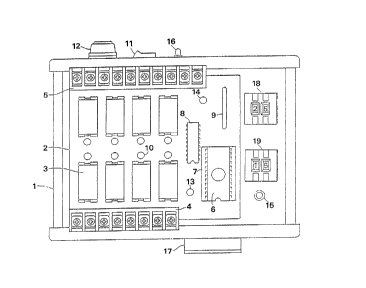
Referring to Figs. 1 and 2, a read-only sequence
controller of the present invention comprises a read
clock pulse control unit 1 having a supply source and an
output relay unit 2 mounted on the clock pulse control
-- 2
.. . ,, . ~.. .. . .. ." .,
: :~ . -: : .. . : . ; ~ : i, . ,,,, ;,,;", , .,. , :,
~; . , I ; , :
': ::: : ,, ' : , ' ' , ~ !: '' . -
' ' ' - ~' ' . '' :. . ,.',: .. ' ,'; ',', ,::, : .. '. :' .
210284~
unit 1.
The output relay unit 2 comprises a board
detachably secured to the control unit 1. A number of
relays 3, such as eight relays are mounted on the board.
Terminal units 4 and 5 are disposed adjacent to the
relay unit 2. The terminal unit 4 has eight terminals
for four relays and the terminal unit 5 has ten
terminals for the other four relays and for an
alternating current power supply. An EPROM 6 is
detachably fixed to a connector 7. Numeral 8 is a
transistor array, and 9 is a connector for the clock
pulse control unit 1 and the output relay unit 2. A ~ --
display 10 employed with an LED is provided by
displaying the operatior~ of each relay.
15On the read clock pulse control unit 1, a power
switch 11, fuse 12 pilot lamp 13 with an LED,
abnormality display 14 with an LED, start switch 15,
reset switch 16, input terminals 17, a preset code -
switch 18 for a main circuit A, and a present code ~ -
20 switch 19 for a sub-circuit B are provided. The preset -~
code switch 18 displays digits of two figures for one
cycle time and is adapted to select a necessary cycle
time. If the unit time for the digits is 0.1 second,
digits "25" of preset code switch 18 shown in Fig. 1
signify a cycle time of 2.5 seconds being set.
Similarly, the preset code switch 19 displays digits
"15" which signify a cycle time of 1.5 seconds.
Referring to Fig. 3 showing a circuit of the
2102844
-
controller, the circuit comprises the main circuit A and
the sub-circuit B which are divided by a dot-dash line
in Fig. 3. The cycle time of the main circuit A is set
to 2.5 seconds by the present code switch 18. The cycle
time of the sub-circuit B is set to 1.5 seconds by the
preset code switch 19. When power switch 11 and reset
switch 16 are depressed, the supply voltage Vcc is
obtained by a switching regulator 20, and a system
supply voltage is applied to an initial reset circuit
21, so that an inverter 22 produces an output at a 1
level. The output is inverted into a 0 level by an
inverter 23 to reset or set each of R-S latches of first
to sixth flip-flops.
When a first flip-flop 24 is reset, a transistor 25
is turned off, causing the output of an inverter 27 to
got to 1 through a chatter preventing circuit 75, and
Schmitt circuit 26. An output of an inverter 28 of the
main circuit A is changed to "0" which is applied to a
CI input of a presettable down counter 29 so that
presettable down counters 29, 30 becomes count enable
states.
A second flip-flop 31 is set through a 2-input NAND
gate 32. A one-shot pulse "0" appears at an output of a
one-shot pulse generating circuit 33.
When a third flip-flop 34 is set through a 2-input
NAND gate 35, a 1 output is applied to an input CE of
the EPROM 6 through the connector 9 so that the EPROM 6
stops producing data.
2102~4
When a fourth flip-flop 36 i8 reset through a
2-input NAND gate 37, the output at a 0 level is applied
to a reset input R of a clock pulse generating circuit
38 to stop the operation thereof. The 0-level output is
further applied to inputs PE of presettable down
counters 40 and 41 through a 2-input NAND gate 39 to
preset the digit "15" of preset code switch 19 in
counters 41 and 40, respectively.
When a fifth flip-flop 42 is reset through a
2-input NAND gate 43, an output at a 0 level is applied
to a 2-input NAND gate 44 as an abnormality signal ~ -
output gate.
When a sixth flip-flop 45 in the main circuit A is
reset through an inverter 46, an output at a 0 level is
15 produced, and an output at a 1 level is applied to -~
inputs PE of presettable down counters 29 and 30 through
a 2-input NAND gate 47 to preset the digit "25" of
preset code switch 18 in counters 30 and 29,
respectively.
The 0 output of the sixth flip-flop 45 is further
applied to a seventh flip-flop 49 through a 2-input NAND
gate 48 and to a clock pulse generating circuit 52
provided with a crystal oscillator through an inverter
50 and a 2-input NOR gate 51 to stop producing clock
pulses~
When the start switch 15 of the main circuit A is
depressed, the sixth flip-flop 45 is set through a
chatter preventing circuit 76 and an inverter 53. Thus,
~ 210284~
an output at a 1 level is applied to a clock pulse
generating circuit 52 through the inverter 50 and the
2-input NOR gate 51.
The output of the clock pulse generating circuit 52
provided with a crystal oscillator, is 10 Hz, as clock
pulses. The clock pulses are applied to clock lines C -
of the presettable down counters 29 and 30,
respectively.
Each time one clock pulse is applied to the
presettable counter 29, the preset count therein
decreases by one. When 25 clock pulses are applied to
the presettable counters, both inputs of a 2-input NOR
gate 54 go to a "0". Thus, the 2-input NOR gate 54
produces one read clock pulse.
On the other hand, when an inverter 55 produces
output "1", a 2-input NAND gate 56 outputs a "0". Thus,
a terminal PE of each presettable counter is applied
with a pulse "1" through the 2-input NAND gate 47. At
this time, the "25" of the preset code switch 18 is
preset again in the presettable down counters 29 and 30.
The output "0" of the gate 56 is further applied to
the set terminal of the seventh flip-flop 49 through an
inverter 57. A command signal of 1 level is applied
from the seventh flip-flop 49 to the sub-circuit B
through a Schmitt circuit 58 and an lnverter 59. At a
moment, the output of the inverter 55 is inverted into
"0" to reset the seventh flip-flop 49 through a 2-input
NAND gate 48. Thus, one command signal is produced.
210284~
The command signal is continuously applied to a reset
terminal R of the second flip-flop 31 of the sub-circuit
B at every 2.5 seconds.
When the second flip-flop 31 is reset, an output at
a 0 lever is applied to the one-shot pulse generating
circuit 33. A one-shot pulse "1" appears at the output
of the circuit 33. This one-shot pulse "1" is applied ~ ~-
to a set terminal S of the fourth flip-flop 36 to
produce an output 1 which is applied to the clock pulse
generating circuit 38. The output thereof is 1000 Hz,
as clock pulses. The clock pulses are applied to clock
lines C of the presettable down counters 40 and 41,
respectively.
The output "1" of the fourth flip-flop 36 is
applied to a 3-input NAND gate 60, and three inputs
thereof go to "1". The gate 60 produces an output at a
0 level which is applied to the terminal CI of the
presettable down counter 40 to produce clock pulses.
Each time one clock pulse is applied to the
presettable counter, the preset count therein decreases
by one. When 15 clock pulses are applied to the
presettable counters, both inputs of a 2-input NOR gate
61 go to a "0". Thus, the 2-input NOR gate 61 produces
one read clock pulse.
The one-shot pulse "1" of the one-shot pulse
generating circuit 33 is further applied to the reset
terminal of the third flip-flop 34, the output 0 thereof
is applied to the terminal CE of the EPROM 6 through the
21028~
connector 9 and the EPROM in turn is set to an output
state.
On the other hand, when the output of the 2-input
NOR gate 61 goes to "1", a 2-input NAND gate 63 outputs
a "0" when an inverter 62 produces output "1". Thus,
terminal PE of each presettable counter is applied with
a pulse "1" through the 2-input NAND gate 39. At this
time, the "15" of the preset code switch 19 is preset
again in the presettable down counters 40 and 41.
Thus, every time 15 clock pulses are applied to the
presettable counters 40 and 41, one read clock pulse is
generated from the gate 63. The read clock pulse is
applied to the clock line C of the binary counter 64.
Accordingly, the binary counter 64 produces outputs
through address lines Ql to Q7, so that the outputs are
applied to the address in the EPROM 6 through the
connector 9.
On the other hand, the EPROM 6 produces a data
signal in response to the address signals, so that
respective actuators of the machine are operated through
relay unit 2.
Time of one cycle is decided by the number of read
clock pulses. Operation in the case of 100 read clock
pulses in one cycle will be explained hereinafter.
In order to produce the one-cycle end signal upon
100 read clock pulses, address lines Q3, Q6 and Q7 of
the binary counter 64 are selected as the inputs of a
3-input NAND gate 65. Since the binary number of "100"
- 8 -
, .: . . . .
21028~
is 1100100, when the 100th read clock pulse is applied
to the input of the binary counter 65, outputs on the
address lines Q3, Q6 and Q7 go to "1" and the 3-input
NAND gate 65 produces a one-cycle end signal "o".
Since the clock pulse of the clock pulse generating
circuit 38 is produced at 1000 Hz, the cycle time of -
the sub-circuit B is 1.5 seconds.
When one cycle is completed, the third flip-flop 34 -
is set through the 2-input NAND gate 35, so that an
output 1 is applied to CE of the EPROM 6 to stop
producing the output. The fifth flip-flop 42 is set
through an inverter 66. A first input of the
abnormality signal output gate of 2-input NAND gate 44
is changed to "1". The one cycle end signal 0 is
applied to the 3-input NAND gate 60, so that a signal at
the "1" level is applied to CI of counter 40 through the
gate 60. The fourth flip-flop 36 is reset through the
2-input NAND gate 37 to stop the clock pulse generating
circuit 38. Thus, each of the actuators of the machine
stops.
When the work product after the manufacturing
process passes the sensor 67 provided at an outlet of
the machine, a signal having a 0 level is applied to the
set terminal of the second flip-flop 31 through an input
terminal 68, chatter preventing circuit 77, Schmitt
circuit 69, inverter 70 and 2-input NAND gate 32. The
fifth flip-flop 42 is reset through 2-input NAND gate 43
to change the first input signal of the abnormality
, .. . .................... . . .. . .
. ; ~. ., ~ . -
,, , ~
- . . . , -
2102~4
signal output gate of 2-input NAND gate 44 into a "0".
Further, the second flip-flop 31 is reset by the command
signal of the main circuit A at the next 2.5 seconds,
thereby re-starting the operations of the sub-circuit B
and actuators of the machine. The operations of the
actuators are continued unless an abnormality occurs.
When a signal from the sensor 67 is not applied to
the second flip-flop 31 at the end of the one cycle
operation, and the command signal is applied to the
second flip-flop 31, both of the inputs of abnormality
signal output gate of 2-input NAND gate 44 go to "1" to
produce an output "0" so that first flip-flop 24 is set. -
Thus, the transistors 71 and 25 are turned on. The
abnormality display 14 emits the light and the inverter ~-
27 produces the output 0. A signal having 1 level which
is inverted through the 3-input NAND gate 60 is applied
to CI of the presettable down counter 40 to stop clock
pulses. The output of the inverter 28 is changed to "1"
which is applied to the presettable down counter 29 to
stop the operations of both counters. The 2-input NOR
gate 51 produces the output "0" to stop the clock pulse
generating circuit 52. Thus, the output of the clock
pulse stops and the machine completely stops.
After inspection and repair of the machine are
done, the reset switch 16 is depressed and the start
switch 15 is depressed, so that the machine starts
operation.
A terminal 72 is provided for connecting other
-- 10 --
~ 21028~
sequence controllers so as to stop the operation
thereof.
Fig. 4 shows another embodiment. The output of the
clock pulse generating circuit 52 of the main circuit A
is obtained by dividing the output of the clock pulse
generating circuit 38 of the sub-circuit B into 1/100.
The other structures of this embodiment are the same as
the previous embodiment of Fig. 3 except for the
inverter 50 and the 2-input NOR gate 51, and the
descriptions thereof are omitted.
The sequence read-only controller of the present
invention has a weight of 420g. The controller is
mounted on a press machine of a capacity of 160t for
automatically operating the machine. The machine is
sequentially operated at three processes with a full
automatic control without abnormality.
In accordance with the present invention, the
sensor is provided on the outlet of the machine for
detecting abnormality at every one cycle. When an
abnormality occurs, the stop control circuit produces
stop signals to stop the machine. In a press machine,
the machine is stopped at a top dead point. Therefore,
there is no danger because of the full automatic
control.
The sequence controller can be used in various
machines such as an assembling machine and a testing
machine to provide effective automatic operations.
While the invention has been described in
- 11 - . - ~
2102~44
conjunction with preferred specific embodiment thereof,
it will be understood that this description is intended
to illustrate and not limit the scope of the invention,
which is defined by the following claims.
.