Note: Descriptions are shown in the official language in which they were submitted.
.
21~3~
Analog Multiplier
BACKGROUND OF TH~ lNv~NlION
1. Field of the Invention - ~
The present invention relates to a multiplier for :
multiplying analog signals and more particularly, to a
multiplier adapted to be arranged on bipolar or Metal Oxide
Semiconductor (MOS) integrated circuits.
2. Description of the Prior Art
Conventionally, a Gilbert multiplier has been employed in
general as a multiplier formed of bipolar transistors. The
Gilbert multiplier has such a structure that transistor pairs
are provided in a two-stage stacked -nner as shown in Fig~
' :,: ' '~ ;:~
The operation thereof will be explained below.
': -
In Fig. 1, an electric current (emitter current3 IE ~f a p-n
junction diode ~orming a transistor can be expressed by the
following equation (1), where I~ is the saturation current, k is
Bolt -nn's constant, q is the uni~ electron charge, V~F is base-
to-emitter voltage of the transistor and T is absolute ~ ;
temperature.
IE = I5 ~eXP{(qVBE)/(kT)} - 1] (1)
~ ~:
, .~
2~33~)
Here, if VT kT/q~ as VBE ~ VTI when exp~V8E/VT) ~1 in the
equation (1), the emitter current IE can be approximated as
follows;
IE ' IS eXP(VBV/VT) (2)
As a result, collector currents IC43, IC4~, IC4~, IC4~IC4l and
IC42 of the transistors Q43, Q44, Q45, Q46, Q41 and Q42 can be
e~pressed by the following equations (3), (4),(5), (6), (7) and
(8), respectively;
C43 = ~F IC41
ltexp(- V
T
aF ' IC~1 (4)
l+exp~ Vl)
IC45 = aF IC~2
l+exp( 41 ) ~
VT ;:;
a ~ I z ( 6)
exp(- V~
: 2
3 3 0 ~
IC41 = V ( 7 )
l~exp(- 42)
IC~2 = aF Io
l~exp ( 42)
In the equations (3), (4), (5), (6), ( 7 ) and (8.), V41 is an
input voltage of the transistors Qg3, Q44, Q45 and Q46, V42 ~
an input voltage of the transistors Q41 and Q42, aF is the DC
co ~II-base current gain factor thereof.
,::
Hence, the collector currents IC43, IC44, IC46 and IC4B of the
trans~istors Q43, Q44, Q45 and Q46 can be expressed by the
foIlowing equations (9), (10), (11~ and (12), respectively,
2 :: :~
IC43 = ~ ~ I V (g) ~ ~;
1texp(- 41) }{ l~exp(- 42) }
Vll VT
a2, IO ~-
{ l ~exp( 41) }{ l~exp(- 42) ~ ~10) ;
VT VT :
: ~ ~ : 3
'
2~33
{ l+exp( 41 ) } ( l~exp( V92 ) 3
~C46 ~ ~F Io V ( 12 )
{ltexp~- Vl) }{ltexp( v2) }
As a result, the differential current ~I between an output
current IC43-46 and an output current Ic44_4~ can be expressed as the
~ollowing equation (13); ~:
~ I - IC43 45 - IC44-46
= ( ~C43 + IC45 ) - ( IC~4 + IC46 )
= ( IC43 - IC~6 ) - ( I~4 - IC45
= a2 ~ I~ { tanh( 2v ) }{ tanh( 29v )
Here, tanh x can be ~p~n~e~ in series as shown by the
following equation (14) as;
tan~ = X X3 (14) :~
I'hen, if Ixl <~ 1, it can he approximated as tanh x - x.
Accordingly, if ¦V~1¦ <~ 2VT and ¦ V42 1 ~ 2VT, the
differential current QI can be approximated by the following
21~33~)~
equation (15);
~I 40 ( ~vF)2 V~l- V42 (15)
From the equation (15), since the differential current ~I
contains a product of the input signal voltages V41 and V~2, it
can be ~ound that the circuit shown in Fig. 1 becomes a
multiplier for the input voltage voltages V41 and V42.
:: :
Next, with a multiplier formed of MOS transistors, a lot of
sorts of multipliers have been developed for the recent ten
years. One of these conventional MOS multipliers is that
proposed by Z. Wang, which can be considered to be put to
practical use. This multiplier is disclosed in IEEE JOURNAL OF
S~LID-STATE CIRCUITS, Vol.26, No,9, September 1991 entitled "A
CMOS Four-Quadrant Analog Nultiplier with Single-Ended Voltage
Output and Improved ~emperature Performance", so that
description about it is omitted.
The conventional Gilbert multiplier as explained above has
such the transistor pairs stack~d in two stages, so that there
arise such a problem that the power source voltage cannot be
decreased.
Besides, the conventional multiplier proposed by Z. Wang has
a330~
such a problem that its circuit scale is very large since a lot
of current mirror circuits are employed.
SUMMARY OF THE lNY~NlION
Accordingly, an object of the present invention is to
provide a multiplier capable of reducing a power source voltage.
Another object of the present invention is to provide a
multiplier which is simple in circuit configuration.
A multiplier according to a first aspect of the present
invention contains first and second squaring circuits. The
first squaring circuit has first and second diPferential
transistor-pairs, differential input ends and differential
output ends. The seaond squaring circuit has third and fourth
differential transistor-pairs, differential input ends and
differential output ends.
A positive one of the differential output ends of the first
squaring circuit and an oppo~ite one of the differential output
ends of the second squaring circui~ are coupled together. An
opposite one of the differential output ends o~ the first
squaring circuit and a positive one of the differential output
ends of the second squarlng circuit are coupled together. The
output ends thus coupled together constitute a pair of
-- 2L03~VO
differential output ends of the multiplier.
Sum of first and second inpu~ voltages is applied to the
differential input ends of the first squaring circuit, and
difference of the first and second input voltages is applied to
the differential input ends of the second squaring circuit.
A first direct current (DC) voltage is applied between a
first input end of the first difEerential transistor-pair and
a first input end of the second differential transistor-pair.
A second DC voltage is applied between a second input end of the
first differential transistor-pair and a second input end of the
second differential transistor-palr. The second DC voltage is
applied equal in polarity to the first DC vol~age.
A multiplier according to a second aspect of the present
invention contains first, second, third and fourth differential
transistor-pairs.
First output ends of the first to fourth differential
transistor-pairs are coupled together and second output ends of
the first to fourth differential transistor-pairs are coupled
together. The first output ends and second output ends thus
coupled together constitute a pair of differential outp~lt ends
of the multiplier.
A first input voltage superposed on a first reference
~ ~33~)
voltage, which are opposite in phase to each other, i5 applied
in common to the first input end of the first difEerential
transistor-pair and the second input end of the third
differential transistor-pair. The first input voltage
superpo~ed on a first reference voltage, which are equal in
phase to each other, is applied in common to the first input end
of the second differential transi~tor-pair and the sPcond input
end of the fourth differential transistor-pair.
A second input voltage superposed on a second reference
voltage, which are equal in phase to each other, is applied in
common to a second input end of the first differential
transistor-pair and a first input end of ~ihe fourth differential
transistor-pair. The second input voltaye superposed on the
second reference voltage, which are opposite in phase to each
other, is applied in common to a second inpu~iend of the second
di~ferential transistor-pair and a first input end of the third
differential transistor-pair. The ~econd reference voltage is
different in value from the first reference voltage.
A multiplier according to a third aspect of the present
invention contains first, second and thlrd squarirlg circuits.
The first squaring circuit has first and second differential
transistor-pairs, differential inpu~ end~ and differential
'~ ",. .,'~',' ~,; ,', 1 , ~ ,;' ~ ~ ,
3 0 ~
output ends. The second squaring circuit has third and fourth
differential transistor-pairs, differential input ends and
differential output ends. The third squaring circuit ha~ fifth
and sixth differential transistor-pairs, differential input
ends and differential output ends.
A positive one of the differantial outpu~ ends of ~he first
squaring circuit and opposite ones of the differential output
ends of the second and third squaring circuits are coupled
together. An opposite one of the differential output ends of
the first squaring circuit and positive ones of the differential
output ends of the second and third sqiuaring circuits are
coupled together. The output ends thus coupled constitute a
pair of differential output ends of the multiplier.
Difference of first and second input voltages is applied to
the differential input ends of the first squaring circuit, and
sum of the ~irst and second input voltages is applied
respectively to the po~itive ones of the differential input ends
of the second and third squaring circuits. The opposite ones
oP the differential input ends of the second and third squaring
circuits are held at cons~ant electric potentials,
respectively.
With the multiplier according ~o the third aspect,
,'~ " : ~",
2103313~
preferably, a four~h squaring circuit is provided, which
contains seventh and eighth differential transistor-pairs,
differ~ntial input ends and differential output ends. Positive
and opposite ones of the dif~erential output ends of the fourth
squaring circuit are connected respectively to positive and
opposite ones of the differential output ends of the first
squaring circuit. The differential input ends of the fourth
squaring circuit are coupled together to be held at a constant
electric potential. The fourth squaring circuit serves to
remove a DC component from an output of the multiplier.
With the multipliers according to the first and second
aspects, there are provided with the first to fourth
differential transistor-pairs arranged so-called in a line
transversely, not in a stack manner, to be driven by the same
power source voltage. With the multiplier according to the
third aspect, there are provided with the first to sixth
differential tran~istor-pairs arranged and to be driven
similarly.
Additionally, the first to fourth or sixth differential
transistor-pairs are applied with the first and Aecond input
voltages superposed on the positive or negative DC voltage ~bias
voltage~ to obtain the square-law characteristic.
1~
~3~
As a result, the multipliers of the first to third aspects
can be operated at a lower power source voltage than that in the
prior art, and they are simple in circuit configuration since
they are basically composed of the differential transistor-
pairs arranged in a line transversely.
In addition, the respective differential transistor~pairs
may be composed of the minimum unit transistors, so ~hat the
multipliers of the first to third aspects are suitable for high-
frequency operation.
~'
BRIEF DESCRIPTION OF THE DRAWINGS
Fig. 1 is a circuit diagram of a conventional multiplier
formed of bipolar transistors.
Fig. 2 is a block diagram of a multiplier according to first
and second embodiments of the present invention.
Fig. 3 is a circuit diagram of a squaring circuit used for
the multiplier according to the first embodiment, which is
formed of bipolar transistors.
Fig. 4 i~ a diagram showing th~ differential output current
characteristic of the multiplier of the first ~ ho~i -nt.
Fig. 5 is a diagram showin~ th2 transconductance
characteristic of ~he multiplier of the first embodiment.
~: 2~3~01~
Fig. 6 is a circuit diagram of a s~uaring circuit used for
the multiplier according to the second embodiment, which i~
formed of MOS transistorsO
Fig. 7 is a diagram showing the differential output current
characteristic of the multiplier of the second embodiment.
Fi~. 8 is a diagram showing the transconductance
characteristic of the multiplier of the second embodiment.
Fig. 9 is a circuit diagram of a multiplier according to a
third embodiment, which is Pormed of bipolar transistors.
Fig. 10 is a circuit diagram of a multiplier according to a
fourth ~ ~o~; nt, which is formed of MOS transistors.
Fig. 11 is a block diagram of a multiplier according to a
fifth embodiment of the present invention.
Fig. 12 is a block diagram of a multiplier according to a
sixth embodiment of the present invention.
Fig. 13 is a diagram showlng ~he differential output current
characteristic of the multiplier of the sixth embo~i ~nt.
DETAILED DESCRIPTION OF THE ~K~ ~ EMBODIMENTS
Preferred embodiments oP the present invention will be
described below while referring to Figs. 2 to 13.
[First Embodi -nt~
12
2 ~ 3 t~ ~
Figs. 2 to 5 show 3i multiplier according to a first
embodiment of the present invention, which is formed of two
squaring circuits.
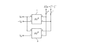
In Fig. 2, first and second squaring circuits 1 and 2 are
the same in circuit configuration, each of which has a pair of
differential input ends and a pair of differential ou~put ends.
Positive t~) one of the differential output ends of the first
squaring circuit 1 and opposite (-) one of the differential
output ends of the second squaring circuit 2 are coupled
together, and opposite ~-) one of the differential output ends
of the first squaring circuit 1 and positive ~+~ one of the
differential output ends of the second squaring circuit 2 are
coupled together. These respective output ends coupled
together constitute a pair of differential output ends of the
multiplier.
In the first squaring circuit 1, a first input signal
(voltage: Vx) is applied to the pos.itive (+) one of the
differential input ends and a signal (voltage: - Vy) opposite in
phase to a second input signal (voltage: Vy) is applied to the
opposite (-) one of the differential input ends. Thus, the sum
voltage (V~ ~ Vy~ of the first and second input signals is
applied across the differential input ends.
~ 13
~ - 2:1 ~33~
In the second squaring circuit 2, the first input signal is
applied to the positive (+) one of th~ differential input ends
and the second input signal is applied to the opposite (-~ one
of the dif$erential input ends. Thus, the difference voltage
(V~ - Vy~ of the first and second input signals i~ applied across
the differential input ends.
The output ends of the first and second squaring circuits
1 and 2 are connected as above, so ~hat output currents I+ and
I- derived from the respective differential output ends of the
multipl.ier are subtracted each other. Therefore, a differential
output current ~IM Of the multiplier is expressed as the
following equation (16);
~ IM = I+ - I~
-- A(V,C ~ VY)2 -- A(VX -- VY)2
= 4A VX-VY (16)
That is, the different:ial output current ~IM is
proportional to the product (V~-Vy) of the first and second input
signal voltages Vx and Vy~ which means that the circuit
comprising the squaring circuits 1 and 2 as shown in Fig. 2 has
a multiplier characteri~tic.
14
' ~- 21~33Q~)
Next, the configuration of the first and second squaring
circuits 1 and 2 is shown below. Since the circuits 1 and 2 are
the same in configuration, only that of the cireuits 1 is
described here.
Fig. 3 shows the squaring circuit 1 concretely, which is
formed of bipolar transistors. In Fig. 3, The circuit 1 is
comprised of a first differential pair driven by a first
constant current source 13 (current: Io) and a second
differential pair driven by a second constant current source 14
(current: Io)~ The first differential pair is composed of
bipolar transistors Q1 and Q2 whose emitters are connected in
common to the first constant current source 13. The second
differential pair is composed of bipolar transistors Q3 and Q4
whose emitters are connected in common to the second constant
current source 14.
Collectors of the transistors Q1 and Q4 are coupled together
and those of the transistors Q2 and Q3 are coupled together.
These collectors thus coupled togekher constitute a pair of
dlfferential output ends of the squaring circuit 1,
respectively.
Bases of the transistors Q1 ~nd Q4 constitute a pair of
differential input ends of the squaring circuit 1, and th~ fir~t
21~33~J
input voltage V1 is applied therebetween.
There is a first DC voltage source 11 whose supply voltage
is V~ between the bases o~ the transistors Q1 and Q3. A
positive (~) end of the firs~ voltage source 11 is connected to
the base of the transistor Q3 and a negative (-) end thereof is
to the base of the transistor Q1. Similarly, ~here is a ~econd
DC voltage source 12 whose supply voltage is the same as that of
the voltage source 11, or V~, between the bases of the
transistors Q2 and Q4. A positive (+) end of the voltage source
12 is connected to the base of the transistor Q2 and a negative
(-) end thereof is to the base of the transistor Q4.
Therefore, a ~irst DC bias voltage Vk is applied across the
bases of the transistors Q1 and Q3 and a second DC bias voltage
Vk, which is equal in value ~o the first one, is applied across
the bases of the transistors Q4 and Q2. The first and second
bias voltages are applied in the same polarities.
Operation of the squaring circuit 1 is as follows;
If the DC common-base current gain factor of the transistors
Q1 to Q4 is expressed as aF, collector currents IC1 and IC2 of the
transi~tors Q1 and Q2 can be expressed as the following
e~uations (17-1) and (17-2);
16
r~
i ". '.
. ~ . - . . : . . . -
?~ 3 ~ 0
= a - I ~17-~)
ltexp(- lV ~)
IC2 = ~F ~ Io (17-2
ltexp( lV ~)
The collector currents IC1 and IC2 satisfy the following equation
(~8).
aF Io = Icl + Ic2 (18)
Hence, a differential output current ~I1 of the first
differential pair can be expressed as follows;
:
~Il = IC1 -- Ic2
= ~F Io tanh{(Vl + V,~)/(2VT)} (19) ,.
:
Similarly, a differential output current ~I2 of the second
differential pair is expressed as follows;
2 = IC3 - Ic~
~F - IO tanh{ ( V1 ~ VK) / ~ 2VT) } ( 20 )
~: .
- ' 17
21~3~3~
where Ic3 and Ic4 are collector currents of the transistori Q3
and Q4, respectively.
Then, a differential output current ~I~Q1 Of the squaring
circuit 1 as shown in Fig. 3 can expressed as follows;
QISQI = (Ic1 + Ic~ C2 + Ia3)
= (ICI - IC2) - (IC3 - IC4)
I 2
~iF Io[t~hl(Vl -~ VK) / ~ 2VT) } - tanh{(V1 ~ V~)/( 2VT) } ] ( 21 )
Here, tanh x can be expanded as shown in the equation (14)
when ¦x¦ ~ 1, so that when ¦V1 + Vk¦ ~ 2VT and ¦V1 Vk¦ ~< 2VT ~
the e~uation ( 21 ) becomes as shown by the followlng equation
(22);
SQ1~F IO [ { K ~ l + V~ ) 3
{ V1 ~ VK 1 ( V1 t VK) 3 } ]
2VT 3 2VT
UF I~ { V 3 ( 2V-) ~ 3 V1 }
T T 4VT
~F IO VK { 1 - 1 (--) - -- }
VT 12 VT 4VT (22
From the equation (22), it is seen tha the differential :~:
18
' 2:~33~
output current ~ISQl is proportional to the square of ~he inpu~
voltage Vl. Accordingly, it can be found that the squaring
circuit 1 has the square-law characteristic.
By the same way, a differential output current of the second
squaring circuit 2, which ~s applied with the second input
voltage V2, can be obtainPd as follows;
~ ,I = aF IO V~ ( V~2 Va 3 (a3)
When the respective differenkial output ends of the first
and second squaring circuit l and 2 are connected to each other
as shown in Fig. 2, the differential output current ~IM Of the
circuit thus obtained is given as;
= ~ISQ1 ~ ~ISQ2
~aFI~3V~ (v2-V22) (24)
4 VT :
.' ..
Here, the voltages V1 and V2 are expressed as Vl = V~ + Vy and
V2 = V~ - V~, respectively, then the diEferentia} output current
~I~ of the multiplier of the first embodiment can be obtained a~
the following equation (25);
: 19
3 3 0 ~
a p IO VK V V ( 2 5 )
Similar to the equation (16), it is seen that from the
equation (25) the differential output current ~IM Of the
multiplier is proportional to the product (V~-Yy) o~ the first
and second input signal voltages V~ and Vy~ Accordingly, a
multiplication result of the input voltages V~ and Vy
can be obtA;ne~ from the differential output current ~IM.
Fig. 4 shows a relationship between the differential output
current ~IM and the first input voltage Vx, in which the second
input voltage Vy is a parameter and Vk = 2.35 VT. Fig. 4 was
obti~;ne~ based on an expre~sion of the differential output
current ~IM~ which is different from that j.n the equation (25).
This expression Of ~IM was given by using the equakion (21)
including the hyperbolic tangent function.
Fig. 5 shows the transconductance characteristic of the
multiplier, in which the second input voltage Vy is a parameter
and V~ = 2 . 35 VTI similar to Fig 4. The transconductance
~d~IM/dV~) was obtained by di~ferentiating the expression of AIM
used for obt~ining Fig. 4 by the first input voltage V~. It is
seen fr~m Fig. 5 that when Vk = 2.35 VT ~he transconductance of
~ 20
2 ~ 3 ~ ~
the multiplier becomes maximally flat.
Although not shown, the transconductance characteristic
becomes a curve having a single peak when Vk ~ 2.35 VT~ and that
having twin peaks when V~ > 2 . 35 VT~
As described above, with the multiplier according to the
first embodiment, there are provided with four differential
pairs arranged so-called in a line transversely to be driven by
the same power source voltage and the differential pairs are
applied with the first and second input voltages V~ and Vy
~uperposed on the DC bias voltages Vk to obtain the square-law
characteristic. Asia result, the multiplier can be operated at
a lower power source voltage as well as simple in circuit
configuration.
In additionj since the respective differential pairs may be
c~ sed of the minimum unit transistors, the multiplier is
suitable for high-frequency operation.
[Second Embodiment]
Fig. 6 shows a squaring circuit 1' used for a multiplier
according to a second e~bodiment, in which MOS transistors M1,
M2, M3 and M4 are employed instead of the bipolar transiistors
Q1, Q2, Q3 and Q4 in ths squaring circuit 1 of the first
; 21
2~33~ :
embodiment. The interconnection of the MOS transistors Ml to
M4 is the same as that of the squaring circuit 1.
The squaring circuit 1' is comprised of a ~irst differential
pair driven by a first constant current source 13' (current: Io)
and a second differential pair driven by a second constant
current source 14' (current: Io)~ The first differential pair
is composed of the MOS transistors M1 and M2 whose sources are
connected in common to the first constant current source 13'.
The second dif~erential pair is composed oP MOS transistors M3
and M4 whose sources are connected in common to he second
constant current source 14'.
Drains of the transistors M1 and M4 are coupled together and
those of the transistors M2 and M3 are coupled together. These
drains thus coupled together constit~te a pair of differential ;i~
output ends of the squaring circuit 1', respectively. ;~
Gates of the transistors M1 and M4 constitute a pair of
differential input ends of the squaring circuit 1', and a first
input voltage V~ is applied therebetween.
There is a first DC voltage source 11' whose supply voltage
ig Vk between the gates of the transiYtors M1 and M3. A
positive (~) end of the first voltage source 11' is connected
to the gate of the transistor M3 and a negative (-) end thereof
22
~ : ".
2~a33a~
is to the gate of the transistor ~1. Similarly, there is a
second DC voltage source 12' whose supply voltage is the same
as that of the voltage source 11', or Vx, ~etween the gates of
the transistors M2 and M4. A positive (~) end of the voltage
source 12' is connected to the gate of the transistor M2 and a
negative (-) end thereof is to the gate of the transistor M4.
Therefore, a first DC bias voltage V~ is applied across the
gates of the transistors M1 and M3 and a ~econd DC bias voltage
Vk, which is equal in value to the first one, is applied across
the yates o~ the transistors M4 and M2. The first and second
bias voltages are applied in the same polarities.
Operation of the squaring circuit 1' is as follows;
If the MOS transistors M1, M2, M3 and M4 are operating in
the saturation region, differential output currents AIl of the
first and second differential pairs can be expressed as the
following equations (26-1) and (26 2), respestively;
~II = 2l/2 Io(Vi/VU) [1-{Vl2/(2Vu)}] ¦Vi¦SVu (26-1)
~II = Io sgn(V~ SVU (26 2)
. .
~ 2~33~
where i = 1 and 2.
In the equations (26-1~ and (26-2~, Vu is expressed as Vu =
(Io/~)1/2 by using the transconductance parameter ~, and ~ is
expressed as ~ = (1/2)~ Co~(W/L) where ~ is the effective surface
mobility, CO~ is the gate~oxide capacity per unit area, W is the
gate width and L is the gate leng~h of the MOS transistor.
The equation ~26-1) can be approximated by the following
equation (27).
f ( Vi ) = ~ Io { vi - ( 1 ~ ~ ) 3 J (27)
I ~ Vu ~ ~,
The equation (27) is in inaccuracy or error within 3 % with
respect to the equation (26-1) which is obtained based on the
square-law characteristic of the ~OS transistor when IVil ~ Vu.
The values obtained through the SPICE simulation using
Shockley's Equation is also in inaccuracy or error within 3 %
with respect to the equation (26-1) when IV1l S Vu, however, the
inaccuracy or error between the simulation values and the
equation (27~ is better than that between the simulation values
and the equation (26-1). Therefors, the equat.ion (27) i~ better
24
2:1~33~)
in approximation than the equation (26-1) and as a result, the
equation (27) is very good approximation for the purpose of
providing the input-output characteristic of the MOS
differential pairs.
Then, when V1 is expressed as V~ = V1 ~ Vk in the equation
(Z6-1), a differential output current QIS~I of the first and
second differential pairs is given as;
~Isp~ I2 2
{ V1 t VK 1 ( V1 + VK )
~ VU ~ 2 V~
_ V1 VK 1 ( V1 VK )
2VU2 (28) ~:
¦ Vl - VK I ~ VU
If the equation (27) is substituted into the equation (28),
the differential output current QI5QI can be given as the
following equation (29);
hIsQl . 2¦~Io { v~ ) 3 ) t29)
u ~ 'u
: 25
.
,, . ! ~
~';'' 2~Q3~a~)
It is seen that from the equation (29) the differential
output current ~IgQ1 is proportional to the square of the input
voltage Vl, which means that the circuit shown in Fig. 5 has the
square-law characteristic.
The multiplier according to the second embodiment contains
two of the squaring circuits 1' shown in Fig. 5 as the squaring
circuits 1 and 2 in Fig. 2, so that the differential output
current ~I~ of the multiplier can be given as;
~ IM = ~ISP1 ~ ~ISP2
- -6 ~ Io ( ~ 3( Vl ~ V2 ) ~30)
VK I ~ VU
Here, similar to the first emho~; -nt, the voltages V1 and
Vz are expressed as Vl = Vx ~ Vyiand V2 = V~ - Vy~ respectively,
then the equation (30) bec~r ?S as the following equation (31);
Ql 24~ 1 ) V~r ( V V ) (31)
¦ VX ~ VY ~ VK I ~ VU
It is seen that from the equation (31) the dlfferential
output current ~IM is proportional to the product (Vx-Vy) of the
26
:
.~. 2la330~
first and second input voltages V~ and Vy~ which means that the
multiplication result is derived from the current ~
Fig. 7 shows the differential output current characteristics
of the multiplier of the second embodiment, in which the solid
lines show the differential output current ~IM obtained from the
equations (26-1) and (26-2) and the alternate long and short
dash lines show that obtained approximately from the equation
(27). It is seen that from Fig. 7 the approximation using the
equation (27) is considerably good.
Fig. 8 shows the transconductance characteristic of the
multiplier, in which Y~ = 0.761 Vu. I~ is seen from Fig. 8 that
when Vk = 0.761 Vt,the transco~uctance of the multiplier becomes
approximately linear.
There can be provided with the same advantages or effects
as those of the first embodiment.
[Third ~mbodlment]
Fig. 9 shows a multiplier according to a third embodiment
of the present invention, which comprises four differential
transistor-pairs driven by respective constant current sources.
In Fig. 9, a fir~t diEferential pair is c~:,osed of bipolar
transistors Q1' and Q2' whose emitters are co~nected in c- en
27
..... ...
--' 21~30~
to a first constant current source 27 (current: Io)~ A second
differential pair is composed of bipolar transistors Q3' and Q4'
whose emitters are connected in common to a secund constant
current source 28 (current: Io)~ A third differential pair is
composed of bipolar transistors Q5' and Q6' whose emitters are
connected in common to a third constant current source 29
(current: Io)~ A fourth differenti~l pair is composed of
bipolar transistors Q7' and Q~' whose emitters are connected in
common to a fourth constant current source 30 (current: Io)~
Collectors of the transis~ors Q1', Q3', ~5' and Q7' which
belong to the first, second, third and fourth differential
pairs, respectively are coupled together to form one of a pair
of differential output ends of the mul$iplier. Similarly,
collectors of the transistors Q2', Q4', Q6' and Q8' which belong
to the first, second, third and fourth differential pairs,
respecti~ely are coupled together to form the other of the pair
of differential output ends of the multiplier.
A first input signal voltage -(1/2)V~ from a ~irst signal
source 23 is superposed on a first reference voltage V~ from a
first reference voltage source 21, which are opposi~e in phase
to each other, to be applied to a base of the transistor Q1' of
the first differential pair and to that of the transistor ~6'
28
-- 21~30~
of the third differential pair. :~
The first input signal voltage (1/2~Vx from a second signal
source 24 is superposed on the first reference voltage V~, which
are equal in phase to each other, to be applisd to a base of the ~-
transistor Q3' of the second differential pair and that of the
transistor Q8' of the fourth differential pair.
A second input signal voltage -(1/2)Vy from a third signal
source 25 is superposed on a second reference voltage (V~ ~ V~),
which are opposite in phase to each other, to be applied to a
base o~ the transistor Q4' of the second differential pair and
to that of the transistor Q5' of the third differential pair.
The second reference voltage (V~ + V~) is generated by the first
reference voltage source (Yoltage: VQ) 21 and a second reference
voltage source (voltage: Vx) 22.
The second input signal voltage (1/2)Vyfrom a fourth signal
source 26 is superposed on the second reference voltage (V~ ~
V~), which are equal in phase to each other, to he applied to a
base of the transistor Q2' of the first differential pair and
that of the transistor Q7' oE the fourth differential pair.
In the multiplier having the above-identified
configuration, differential input voltages VI~ VII~ ~III and VIY
of the first to four h differential pairs are given as the
29
G ~ G;
- 2.~ ~33 ~
following expressions, respectively;
VI { ( 1/2 ) ( V,~ + VY ) } -- VK ( 32~
VII = {1j2)(VX + Vy)} VE (32-2)
VIII= { ( 1/2 ) (V,~ -- VY) } + V~ ( 32--3 ) : :
VIV = -{(1/2~ (V,~ - VY)} + Ve (32-4~ :
Accordingly, a differentlal outpu~ current ~IMI Of the
multiplier can be expressed as the following equations (333;
- 1 ( VX + VY ) VK
~IM = ~F Io[ tanh { 2VT
2 ( VX t VY ) - VK 2 ( VX - VY ) + VK
~ tanh ( 2 VT } t tanh { 2 VT
- 1 ( VX - Yy ) t Vr~
+ tanh ~ 2VT } ]
2 ( Vx t VY ) + VK
= aF Io[ - tanh { 2 VT
2 ( VX + VY ) - VK --( VX ~ VY ) + VK ~:
t tanh ~ 2 VT } t tanh { 2 VT :
2 ( VX VY ) - VK
; - tanh { 2VT } ] (33) :~ :
~ 30
2 ~ 3 3 0 ~)
It is seen that from the equation (33) the differential
output currenti~IM' is expressed by two terms made of difference
between two hyperbolic tangent functions, which means that the
first to fourth differential pairs provide the square-law
characteristics, respectively.
Accordingly, if tanh is exp~n~e~ by using the equation (14),
when l(1/2)(V~ + Vy) - V~¦ ~ 2VT and ¦ (1/2) (VX ~ YY) - V~l ~ 2VTI
the equation (33) is changed ko the following expression (34)
through the isame approximation as used for obtaining the
equation (25).
aF IO VK V V ( 34)
gV~
It is seen that from the expression (34) the dif~erential
output current ~IMI is proportional to product (Vx Vy) of the
first and second input voltages Vx and Vy~ resulting in an
multiplication result thereof.
The equat.ion (34) is the same as the equation (25) except
for a coef~icient (1/4), so that the multiplier of the third
embodiment has the same advantages or effects as those of the ;~
firsit and s~cond embodiments. ~ :~
3~
,:
:;; 2~33~
..
[Fourth Embodiment] -~
Fig. 10 shows a multiplier according to a fourth ~ ho~; ~nt
of the present invention, which employs MOS transistors instead
of the bipolar transistors in the third embo~; -nt.
In Fig. 10, a first differential pair i5 composed of MOS
transistors M1' and M2' whose sources are connected in common
to a firs~ constant current source 27' (current: Io)~ A second
differential pair is composed of MOS transistors M3' an~ M4'
whose sources are connected in common to a second constant
current source 28' (current: Io)~ A third differential pair is
composed of MOS transistors M5' and M6' whose sources are
co~nected in cc -n to a ~hird constank current source 29'
(current: Io)~ A fourth differential pair is composed of MOS
transistors M7' and M8' whose sources are connected in common
to a fourth constant current source 30' (current: Io)~
Drains of the transistors Ml ', M3', M5' and M7' which belong
:
to the first, second, third and fourth differential pairs,
respectively are couplsd together to form one of a pair of
differential output ends of the multiplier. Similarly, drains
of the trans stors M2', M4', M6' and M8' which belong to the
first, second, third and fourth differential pairs,
respectively are coupled together to form the other of the pair i-
32
2~33~ :
of differential output ends of the multiplier.
A first input signal voltage -(1/2~Vx from a first signal
source 23' is superposed on a first reference voltage V~ from a
first reference voltage source 21', which are opposite in phase
to each other, to be applied to a gate of the transistor M1' of
the firs'c differen~ial pair and to that of the transistor M6'
of the third differential pair.
The first input signal voltage (1/2)Vx from a second signal
source 24' is superposed on the firs~ reference voltage VR~
which are equal in phase to each other, to be applied to a gate
of the transistor M3' of the second differential pair and that
of the transistor M8' of the fourth differential pair.
A second input signal voltage -~1/2)V7 from a third signal
source 25 is superposed on a second reference voltage (VRi + VE) ~
which are opposite in phase to each other, to be applied to a
gate of the transistor M4' of the second differential pair and
to that of the transistor ~5' of the third differential pair.
The second reference voltage (V~-~ Ve) is generated by the first
reference voltage source 21' (voltage: VR) and a second
reference voltage source 22' (voltage: Ve).
The second input signal vol~age (1/2)Vy from a ~ourth signal
source 26' is superposed on the second reference voltage (VR
33
,~ " ~ ' " ~
2~3(3~
Ve), which are equal in phase to each other, ~o be applied to a
gate of the transistor M2' of the firs~ differential pair and
that of the transistor M7' of the fourth differential pair.
In the multiplier having the above-iden~ified
configuration, similar to the third embodiment shown in Fig. 9, :
differential input voltages Vl, VII~ VIII and VIV Of the first to
fourth differential pairs are given as the expressions (32-1),
(32-2~, (32-3) and (32-4), respectively;
Accordingly, a differential output current ~I~' of the
multiplier can be expressed as the following equation (35);
~IM = ~ISP1 ~ ~ISP2
. -6~Io ( 1 ~ ) 3 ~ ~ ll 2 ( VX + VY ) 1
- { 2 ( VX ~ VY )
= -6~Io ( 1 - ~ ) 3 VX VY
¦1 ( Vx i Vy ) i VK I ~ U
, ~.
Similar to the second embodiment shown in Figs. 2 and 6,
Prom the equation t35), it is seen that the differential outpuk
current ~I~' is proportional to produc~ (V~-vy) of the first and
second input voltages Vx and Vy~
34
2~33~
The equation (35) is the same as the equation (31) in the
second embodiment except for a coefficient (1/4), so tha~ the
multiplier of the fourth embodiment has the same advantages or
e~fects as those of the second embodiment.
CFifth r ~ t~
Fig. 11 shows a multiplier according to a ~i~th embodiment
of ths present invention, which is ~ormed of first, second and
third squaring circuits 3, 4 and 5. These squaring circuits 3,
4 and 5 are the same in circuit configuration and each o~ them
is composed of the squaring circuit shown in Fig. 3 or 6,
similar to the first embodiment shown in Fig. 2.
In Fig. 11, the first, second and third squaring circuits
1, 2 and 3 have each a pair of di~ferential input ends and a
pair o~ di~ferential output ends. Poisitive (+) one of the
differential output ends of the first squaring circuit 3 and
opposite (-) ones of the differential output ends o~ the second
and third squaring circuits 4 and 5 are coupled together, and
opposite (-) one of the di~ferential output ends of the first
squaring circuit 3 and poisitive (+) ones of the differential
output ends of the second and third squaring circuits 2 and 3
are coupled togPther. These respective output ends coupled
~ .r, ~ i ;~ i, - ~ i, .. ~ ~i
~ rl 1~
together constitute a pair of differential output ends of the
multiplier.
In the first squaring circuit 3, a first input signal
voltage Vx is applied to the positive (~) one of the
differential input ends and a second input signal voltage Vy is
applied to the opposite (-) one of the differential input ends.
Thus, the difference voltage (Vx ~ Vy) of the fi~st and second
input signals V~ and Vy is applied across the di~ferential input
ends.
In the second squaring circuit 4, the first input signal
voltage V~ is applied to the positive (+~ one of the
differential input ands and the opposite (-) one of the
differential input ends is grounded, that is, the opposite one
is held at the earth potential. Thus, the first input signal
voltage V~ is applied across the differential input ends. ;~
In the third squaring circuit 5, the second input signal
vol~age Vy is applied to the positive (~) one of the ;~
differential input ends and the opposite (-) one of the
differential input ends is grounded. Thus, the second input
~ignal voltage Vy is applied across the differential input ends.
With the multlplier having the ~onfiguration as above, a
di~ferential output current ~IMI' of the multiplier is expressed
~ I !; ;~ ,! ~ , ~ ,,,, , 1 ~ ~ ;
-~" 2 ~ '~ 3 ~
as the following e~uation (36) as;
- -A(V - Vy)2 + AVx2 ~ Vy2
= A V~Vy (36)
It is seen that from the equation (36) a multiplication
result of the first and ~econd input signal voltages V~ and Vy
can be obtained from the current ~IMII .
In the fifth embodiment, the input voltage range of the ::~
multiplier is narrower than those of the first and second
- :~
~ embodiments, however, there is an advantage that no negative~
, ~ ., ~ ,.
phase input voltage and no differential input one are rsquired
for all the squaring circuits 3 and 4.
[Sixth Embodiment] ~
Fig. 12 shows a multiplier according to a sixth ~ '~4~i -nt : ~:
of the present invention, which is comprised of a fourth
squaring circuit 6 in addition to the fifth embodiment shown in
Fig. ll. The ~ourth squaring c1rauits 6 is the same in circuit
configuration and is composed of the squaring circuit shown in
~~ Fig. 3 or 6.
,
; 37
.' ,"
~',""..' ..'.'','~'."~'".'""','.."''.''1''"'','' .~ '' ~' '";'
C3 0 ~
In Fig. 12, positive (+) and opposite (-) ones of
differential output ends o~ the fourth squaring circuit 6 are
connected to the positive and opposite ones of the dif~erential
output ends of the first squaring circuit 3, respectively. A
pair of the differential input ends of the fourth squaring
circuit 6 are connected in common to be groundedj that is, are
held at the earth potential.
With the sixth embodiment, there is an advantage that a DC
~omponent of a di~ferential output current ~IM~ +~
of the multiplier can be removed due to the function of the
fourth squaring circuit 6.
An example of the differential output characteri~tics of the
multiplier is shown in Fig. 13. Fig. 13 was obtained by using
the bipolar squaring circuits as shown in Fig. 3 where Ve =
2.35VT. It is seen that ~rom Fig. 13 th0 same characteristics
as those in Fig. 4 are gi~en.
38