Note: Descriptions are shown in the official language in which they were submitted.
21~374~
3DAP'rIVE r)A'~ \TI
... ..
~-K~:T ~`O,UM~NI(-~r~ S
BACKCROUND OF rl~E ~ NVENTI~
1. FIEL~ OF THE INVENTION .
j ~ ~
; The Present inventlon reiates -o ~-ackeT c^mmunlcallGn~ s ems
which Iransmit data alon~ a corlmunica.ionC ^~anne! (from ~tati^~
"~" to sla~ion "B"). ~ feedback nath is Drovided on which station
"B" will inform station "A" when a "valid" packet of data is
received. The "validity" of a received packet will be determined
at station "~" by means of a digital`error control coding (for
example the Cyclic Redundancy Check code CRC-16 or CRC-CCITT. the
popular 16-bit codes used in the United States and Europe
respectivelv). The advantage of the present invention reside in
the way digital error control codin~. sPread-spectrum modulation.
Ij interleavin~. and feedback techniques are utilized such that for
the existing in situ channel conditions a minimum amount of energy
is used to transmit each packet of information by automatically
compensating ~or chan~es in the conditions of the channel.
~ .
2. ~ESCRIPTION OF THE PRIOR ART
~,, .
In the prior art, data communications svstems having feedback
use an Automatic Repeat Request tARQ~ scheme. The three common
.
variants are the Stop-and-Wait ARQ, the Co-Back-~ Continuous ARO,
and the Selective-Repeat Continuous ARQ; variations of these three
common variants also exist. All current feedback error control
2-5 ~ techniques suffer a common disadvantage in that they discard an
entire frame of information if an error is detected.
.. .: . ... , " .. . . .. . . . .... . . . . ... . ... . . . .
2~037~
~ . 5. ?atent ~umber m7;4.211 issued on .~UgUSt )1. 1973 to
Edward ~. Rocher et al discloses a data communications system bv
which blocks are retransmitted wnen no acknowled~ment is received
within a specified period of time.
; Japanese patent number a;-731;7 published February 6. I9gO bv
Kazumasa Kumakura and UK. Patent Application published March 11.
1987 by Takahashi et al disclose the use of an .~CK signal to
acknowled~e the proper receipt of data while a ~o .~CK signal is
sent in response to error corrupted data being received.
U. S. Patent Number 4 ! 803.685 issued February 7. 1989 to
Christian Oget and U. S. Patent Number 4.905.234 issued February
27, 1990 to Jeffrey S. Childress disclose a process to specify
which frames have not been received properly and retransmittin~
those frames.
Ij U. S. Patent Number 4.393.;01 issued July i2. 1983 to Richard
A. Kellogg et al and U. S. Patent .~umber 4.270.20j issued May 26.
1981 disclose data communication systems with variable data rates.
The article by Mark Hewish et al (Defense Electronics
Computing Number 3 ~Editorial Supplement to International Defense
Review. July 1991]) discloses timing signals transmitted by the
Global Positioning System (GPS) usable with the present invention.
None of the above inventions and patents. taken either singlv
or in combination. is seen to describe the present invention as
claimed. ~ -
. .
.
,,,, , - , - : , . .~ ,: . :
2~037 44
SUMMARY OF TI~E I NVENT I ON .: .
~efinition of Terms and Gene}al Backgrouno
- i. In non-spread spectrum digltal communications systems the
minimum "quantity" of information is equal to the transfer "unit":
; both are refereed to as a 'bit .
2. In a spread spectrum digital communications system the
minimum "quantity" of information is a "bit". but the transfer unit
is one "chip", which has some average rractional relationship to a
"bit". Therefore, a plurality of chlps representing one bit is,
transmitted until a correct recognition acknowledgement (CRA);
signal is received by the transmitter. The CRA is sent to the -
transmitter along a feedback path by the receiver after recogni~ing ,~
the bit represented by the plurality of chips received.
3. One can use the time associated with one chip from each
1~ bit of a packet to transmit information over the feedback channel.
In this manner. the transmitter would only transmit one additional
chip after the receiver has already recognized the bit represented
by the plurality of chips before the transmitter would receive the
CRA and start transmitting the first chip representing the next bit
of the frame. For this situation the Throughput Efficiency in
terms of energy utilization required for effective communications
is equal to the Chlp-To-Bit Ratio ~CBR) divided by the quantity one
plus the CBR.
Any random compound error channel (that is a channel that has
a mixture of independent errors and burst errors present) can be : -
transformed into an independent error channel. or what I call a
stochastic communication channel. by using a digital spread-
spectrum modulation and a pseudo random interleaving process. The
result is the distribution of fractional portions of information
3~ ~ throughout the transmission such that any random or periodic noise
burst (with the exception of nolse bursts that correlate with the
-
.. , ., . ,, . . _, . . . . . .. . . . . . ........... . . . . . . .
~1 . ~ , . .
:, : :. : - - . , : : . , : . -:, : . : -
- 2~03~ ~
pseudo random interleaving. or rer~ intelligent jammingi will be
distributed to as man- bits OI information as possible. i noise
burst can have a duration as follows and will have the associated
effect on communications effectiveness:
1. A duration of one chip or less. Very little effect on
the transmission because of the high Chip-To-Bit ratio.
2. A duratio~ of greater than on chip but less than one chip
frame. Very little effect on the transmission because of the high
Chip-To-Bit ratio. The interleaving has spread the e~fect of the
burst out among the bits in the message and thereby prevented a
concentrated effect on one bit.
3. A duration of greater than one chip frame but not beyond
the power of the spread spectrum technique to overcome. Very
little effect for the same reasons stated above.
4. .~ duration in excess of the effectiveness of the spread
spectrum technique in use. The bit level error control codin~
technique will need to be used to identifv the presence of errors.
The effect~veness of the digital error control coding technique is
enhanced because the noise environment appears stochastic rather
than impulsive.
The present invention is a process that utilizes a varietv of
communications techniques in a particular method to provide a
reliable digital packet communications apparatus. These techniques
include di~ital error control coding. spread-spectrum modulation
2; with interleavin~. and feedback techniaues. It is assumed that
each packet will be of fixed size.
In the e.Yamples that follow I have used a frame size of 1400
bits. the chip to bit ratio to overcome thermal noise is assumed to
, be 10, the nominal chip to bit ratio for an avera~e gaussian noise
' environment is 100, and the chip to bit ratio to indicate an
- abnormal system condition requiring operator action will be ten
times the nominal chip to bit ratio or 1000.
- -
Il ' - -- -
., ,.~ . . . , ., ,.,. : ~. . ', ' . .'::' . . '
2~0374~
~he ~ransmjssion Process
In broad terms the transmission Drocess pro,^eeds as follows:
1. A packet isi obtailled from a transmission nuffer.
2. .~ digital error controi code is appended to the packet to
; produce a frame.
3. The frame is modulated by a lonR binarv pseudo random
number (PRN) code (the spread spectrum modulation). In this step
the length of the PRN is such that a sianificant number of chips in
excess of what is expected to be required are produced for each
bit. ~f the original ~i~stem design indicates that a nominal chip
to bit ratio of 100 is e~pected. a modulation process that vields
1000 chip for each bit would not be unreasonable.
4. The spread spectrum chips are interlea~ed to produce chip
frames. This step results in grouDings of chips such that if a
l;frame has 1400 bits then the îirst chip frame ~ould consist Gf 1400
chips ~.vhere the first chip from each of the 1400 bits ~vould
comprise the chip group.
;. The ordering of the chips in each chip frame ls aependent
on another PRN.
,06. The transmitter starts sendin~ the chip frames in
sequence to the receiver station.
7. The transmitter station listens for a Correct Receipt
Acknowled~ment ~CRA) form the receiver station on the feedback
channel.
.55. While the transmitter is sendina ~ne biT frame and
listening for the CRA it prepares the ne~t bit frame for
transmission.
9. When the transmitter detects the CRA on the feedback
`channel it selects the first chip frame from the ne.~t bit frame for
transmission at the conclusion of the current chip frame.
--10. The transmitter repeats steps 7. 5. and 9 until all
packets are transmitted.
.
... ~ .. . . . . . . . .. . . . . . . . .
æ~o3~ 4~
he Rece~ti^,n Process
In broad terms The receplion r,ro.^ess ?roceeds as fr,llows:
1. The recei-er establishes ~-nchrnni_ation with the
transmission station.
, 2. The receiver correlates the chip frames. This i~ the
inverse of steps four and three of the transmission process above.
That is the chips are rearranged in a normal order from their
pseudo random order. and the chips for each bit in the frame
correlated for association to yield a bit determination.
3. After sufficient chips are associated for each bit a bit
determination is made: the result is a bit frame. The
determination of "sufficient" chips is based on man~ factors
includin~ the design minimum chip to bit ratio based on thermal
noise. and evaluation ot` in situ .^onditions based on the preferred
I; s,vnchronization process.
4. The received bit frame from Stêp three above is evalllated
for validit-- based on the error control code that was appended in
step two of the Transmission Process. If the bit frame is
validated The process continues to step five below. if not the
process repeats step three above to obtain another chip frame.
;. Start sending the CRA to the transmission station on the
feedback .:hannel.
~ . Evaluate the succeeding .-hip frames IO detect the
transition IO the ne.~it bit frame. Once tne bit frame transitiGn is
'; detected stop sendin~ the CRA and go ~ step ~wo abo-e.
.. . . . . .
, ' ':
:. '- " ''
6 ~,
.. .. ... _ .. ... . . . .. . , , , ,, , , , , , _
. , , . . . , , . . . . .,, ., .. . ... . , ~ .. . . . . . .. . . . . . . . ..
2~037 ~
!le S!~nchr~ni..~ n Drocess
In the preferred embodiment this 5v5tem~vill o~erate in a full
duple.Y mode. that ls information transmission in hoth dir~-ctions at
the same time. In this condition. both station ~ and station B
; will transmit the svnchronization signal and acknowledgment
information on the -same channel. The receiver must know three
things: first. exactlv when each chip frame starts: second~ eYactlv
how long a chip frame lasts: and third. e~actlv when a first chip
frame of any bit frame starts.
t0 The transmitter station will continuously transmit a si~nal on
the synchronizationifeedback channel. This signal will always have
a period equal to the duration of one chip frame and be constructed
such that the start of each chip frame can be discerned.
Two basic signal constructions are required! with each having four
1~ possible alternate constructions (for 3 total of ten signal
structures)
1. The flrst sequence will indicatë the start of a bit frame
and have a total duration of the bits per frame times the thermal
noise chip to bit ratio (using the e.Yample numbers this would be 10
tlmes 1400 or 14000). This chip sequence would be so constructed
that the e.Yact start point of the sequence could he calculated from
a sample as small as one chip frame 11400 chips~.
. The second sequence will indicate the chip frame timin~
of transmitted information and have the duration of one chip frame
'5 (1400 chips~.
Each of the two sequences described above wilL have four
alternate configurations to indicate cne of four feedback
conditions: correct receipt of a first frame. correct receipt of an
even frame. correct receipt of an odd frame. and correct receipt of
a last frame.
- f
2~3~ 4~ :
.~t nnv point ~n a Transmission and recepli.-,n ~rocess ~nlr one
of the t~vo transmission conditions -an e~isl:. and oni!- one of the
acknowled~ment conditions can .-~ist. Because i ~his hislorical
dependencv reception calculations need onl~ be evallJated for the
; possible choices and the impossible choices can be i~nored.
Accordingly, it is a principal object of the inventic.n to make ~:
a communications channel appear to onl- have gaussian noise present -
even thou~h random impulsive noise is present.
It is another object of the invention to make the
communications channel appear to only ha-e gaussian noise present
even thou~h non-random impulsive noise is present.
It is a further object of the invention to eliminate the need ..
to totally discard transmitted frames of information when an error
is detected in the frame. .
IgIt is a further object of the invention is o d~:namicall~
adjust the data rate throu~h the channel ~o the ,n situ noise ..
conditions. :~.
.~nother object of the invention is to use measured data ratee .
to automatically adjust transmitter power to keeri the.data rates -.
within Prescribed limits.
Yet still another obiect ;,f the ~nventlon is to provide
informa~ion to s-stem operators on the hisloric~l -haracteristics .
of the .ommunications channel. both of a short term duration (the -.
chip to bit ratio required for a particuiar .rame to he sent from
2; one station to anotherl and of lonF duration ~;hannei avera~e chip
to bit ratios that can be used to indicate such thin~s as a~in~
.::
degradation of the system and predictions as ~o vhen correctlre :~ :
action ~ill be required).
It is an object of the invention to provide imDroved elements
and arrangements thereof in an apparatus for the purposes described
--which is inexpensive. dependable and ful~ effective in
accomplishing its intended purposes. -~ -
S ~ .
.. . , _ . _ . ... . . . . . . ..... . . .. . ... .. . .
:, : ......... , : . , . . : , ~ . :
. ,. : ~ . ..
2i~37 44
rhese and other objects o~ ~he 3resenT n~nt .on \\~ll heromte
readii~ apparent upon further r~vie~r~^. the fol!G-~in~ specification
and dra~vings.
BRIEF DESCRIPTION OF THE DRA~INCS
Fi~s. IA and IB are block dia4rams OT the oresent invention.
Figs. 2A-2E are flow charts for the transmission process of
the first embodiment of the present invention.
Fig. 3 illustrates how data s modulated n the first
embodiment of the present invention.
!0 Figs. 4A-4C are flow charts for the reception process of the
first embodiment of the present invention.
Fi~s. ;A-3C are block di~agrams .-~ the various s~stem
confi~urations for the various embodiments of the present
invention.
1; Similar reference characters denote ~orrespondintT f~atures
consistentlv throu~hout the attacned drawin~s.~
: :'' ' '
DETAILED DESCRIPTION OF THE PREFERRED EMBODIMENTS -
::
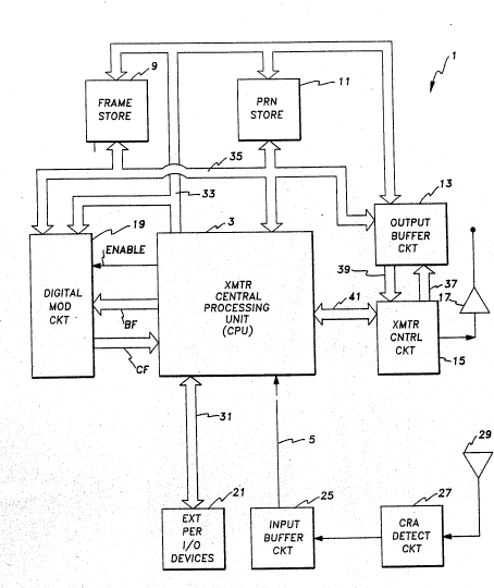
The packet communications svstem for the first embodiment of
the present inventlon utilizes a transmitter .^ontrol s~stem I to
'0 transmit data to a receiver. The transmitter control s!stem I of
~: : :: .
the ~resent lnvention i5 illustrated n ~-t. ;~. The central
processing unit ~CPU) 3 is the main controller for the transmitter
control ;~stem l and includes the necessar~ read onl~ memory (ROM)
random access memorv (R.4M) necessarv. and .^lock si~nals for its :.
~23 ~ ~operation. ` -
. ~ ... . .. . ...... .. . ., : ~ .
~: i ~ :; :
2~03~ 44
~n iddress bus ~3 is used o -.i!o- ~he ~-D~ 3 to ~CC-?'iS
specific porTion of a particular .-l.^uit artached t~erelo. ParT ,.
the address hus 33 is used to speci~~ the parti~ui~r circuit.
another part of the ~ddress bus 33 is used to access a speci ic
portion of the particular circuit. The address bus also contains
a write enable signal which allows the stora~e of information into
the specific portior;of the particular circuit from the data bus 3;
when the write enable si~nal is asserted. v;'hen the ~vrite enable
signal is not asserted. information from the specific area of the
particular circuit addressed is transferred to the ~P~' 3 on the
data bus 35. The transfer of data to and from storage circuitrv as
described above is well-known in the microprocessor art.
rhe irame store 9 is used to store the packets of Information
as frames of bits in the first embodiment. The pseudo-random
1.~ number ~PR:~) store 11 is used to store the various oseudo-random
numbers used in the lirst embodiment to modulate each frame of data
to be transmitted. The digital modulation circuit 19 is usc-d tO
modulate the bit frame or portion thereof provided TO it bv CP~ 3
on the BF data line b~ the portion of a PRN provided to it bv the
?0 ~P~' 3 on the'data bus 3S. Once the dig~tal modulation circuit 19
is accessed by the address bus ~5! and the E~ABLE line is acti~ated
by the ~PU 3. the data on the BF data line is modulated and the
result thereof is produced on the CF data line representin~ the
chip frame data for that portion of the bit frame just modulated.
L~ The bit frames are stored in the output buffer circuit 13 as thev
are modulated. The transmitter control circuit 15 accesses the
output buffer 13 to retrieve data to be transmitted. The
..
transmitter control circuit utilizes and address bus ~7 to access
storage locatio~s vithin the output buffer 13 so as to retr;ere
data on the data bus 39. The address busses 37 and 3j are
- connected to circuitr, within the output bufler !3 so that only one
data bus can access the output buffer memory during an.~- one portion '' -,
10 ' .. , :
.:
2~37 4
of .î ` !ock ~ cie.
Transmitter conl r ol ci.cuil .; ~ran~mit; ~n.- modul3ted bit
frames aiong a data path o. a ^ommun.catir,ns channel ~ia antenna
17. The antenna 79 is used to recei~-e the ~R.~ si~nal ~lon~ a
; feedback path of the communications channel which is sent b~ the
receiver. ~n input buffer circuit 25 is used to store each cl-ip of
the CRA as it is received from the CR.~ detection circuit 27. Data.
Iine 25 is connected to dedicated input ports of the ~PU 3 so as to
transmit the CRA chips stored in the input buffer circuit 2~ when
thev are received by the input buffer circuit '5. Other dedicated
ports include the BF data line. the CF data. the ENABLE line. and
the data bus 41.
The Transmission Process
The al~orithm for the firs~ embodiment of the present
I; . invention ;s described in detail in Fi~ures 2.~ throu~h 2E. Block
101 is the start of the transmission process which ma~ be initiated
in any conventional manner. e.$.. pushins a transmi~ button. Block
102 is performed after the transmission process be~ins and until at
least Gne packet has heen stored within the input buffer circuit 9.
In the first embodiment. the input buffer circuit 9 is provided
~ith data from an e~ternal input Deripheral device '1. In the
first embodiment, the data stored in the input buffer circuit 9 are
the bits which make up each packet. Once it is determined that a
packet of information is available uithin the input buIfer circuit
'~ 19. then a packet is retrieved therefrom as illustrated in block
103. In the first embodiment I will assume that the packet
consists of 1384 bits.
', : ~ :
'
;
2~037 4~ :
The ~acket re~rie~.ed from ~he 'nr,ut ;uff r ~ ^Ui~ t
one o- `our ;:ategories: ~ First PackeI~ an E-~en Packet. an :--di
Packe-.. or ^~ Last Packet. It i~ ~o,si~i. ^;r ~ ^.pec~ asr
occur ~vhere onl.- one packet is in the inDIlt ruffer in which case it
; will be treated as ~ Last Packet teven thou~h It is also ~ First
Packet). Of these four posslble cases onlv two are possible ~ -
options at anv given time based on the tvpe of packet that preceded
it. and of the two possible options one Gf the options is alwavs
the Last Packet option. For e.Yample. if the first pac~et has been
retrieved. then that packet could be a first packet or a last
packét. If the packet retrieved Is the second uacket. then the
packet is either an even packet or a last packet. If the packet
retrieved is the third packet retrieved since the "yes" decision ~ -
was made in block 102, then the packet is an odd packet or a last ~- -
packet, etc. ' ; ~:
For the present discussion, it is assumed that the first
packet is not the last packet in block 4 of Fig. 2A. The ne~t step
lllustrated in biock 105 is to set a counter F to zero for purposes
described below. Afterwards, an error control code is added to the
packet to produce a frame as lndicated by step 106. This bit level ~ -
error control code will be used by the receive station to determine
the validity of the received frame of information. As noted above.
many such codes exist in the prior art such as the CRC-16, or CRC-
CCITT. For illustrative purposes I will assume 16 bits are used by
~the error control~code. Th combination of 1384 bits in the packet :
- : . .
~ with~16 error control bits yields a frame of 1400 bits.
:: ;
In block 107, the spread spectrum modulation and interleaving
process is accomplished. This is the process by which the random
burst component of the compound error channel is effeotively purged
30~ ~ from the system by distributing its energy over the frame. The
preferred method of spread spectrum modulation and interleaving is
conducted as fo.llow~s for the first chip frame: :
: ~ : ... .
~ ~ ~ , 12 ~
. .
` 2io~7 4~ `
1. the first bit of the PR~ modulates the first bit of the
frame ~chip one).
2. the second bit of the PRN modulates the second bit of the
frame (chip two),
3. the third bit of the PRN modulates the third bit of the
frame (chip three),
4. etc., etc:, etc
;. the 1,398th bit of the PRN modulates the t,398th bit of
the frame (chip 1,398),
6. the 1,399th bit of the PRN modulates the 1.399th bit of
the frame (chip 1,399),
7. the 1,400th bit of the PRN modulates the 1.400th bit of
the frame (chip 1,400; the first "chip frame" has now been
modulated)
I; The digital modulation circuit 19 is used to modulate the bit
frame to Benerate the chip frame. Fi~ure 3 illustrates a block
diagram of a portion of the modulation circuit 19. Bit frame data
from the BF data line are stored in frame bit locations I through
Y of memory ;0~ where Y is equal to 1,400 in the first embodiment.
For e~ample, if the BF data line is connected to 16 dedicated ports
of the CPU 3 and the digital modulation circuit. then the BF data
line would have to be loaded 58 times to completely store all 1,400
its of the frame, wherein during the eighty-ei~hth time only half
of the BF data is left~. The PRN data is loaded into chip
~generators 31 from the data bus 35 in the~same manner as the memory
ci~rcu`its 30 are loaded. ~Both memory cirouits ;0 and chip generator
circuits ;l are accessed by the address bus 33 so that the bit
frame data and PRN data are stored at the same time.
~ ` :
~ 13
. ~ . ~ . . . ... . .. . .. . ..... . . . , ... . _ . . . . .
2~.037 4~ :
The chip generator circuits jl ha~e stora~e locations to store -
the PRN oits and also have e.Yclusi~e or (~OR) logic -ircuitr, to
produce an output upon receiving the E~ABLE signal so as to ~OR
each bit frame with the appropriate chip frame as discussed above,
; thereby producing the modulated bit frame as the chip frame data.
The chip frame data is stored in memory circuits ;2. If the CF
data line has 16 dedlcated ports connecting the digital modulation
circuit 19 and the CPU 3, then the address bus will have to access
the chip frame eighty-eight times, wherein during the eighty-eighth
10time only half of the memory circuits ;1 are accessed. e.i. only ,~
eight bits of information would be transferred to the CPU 3.
In block 108r the order of the chips is scrambled in ;
accordance with a "chip frame" PRN. In this manner the first chip ~ ,- -
,may be located in the eighth chip location or some other location. ;~
15The objective here is similar to that in step 107 except this step , ~ -
is specifically designed to counter burst noise that is in
synchronization with the chip frame structure (that is jamming).
This is the process by which the cyclic synchronized burst
component of the compound error channel is effectively purged from -~
20the system by distributing its energy o~er the frame. For example,
lf the synchronlzed bur~st component tends to occur in the eighth -
chip frame componentr then for the first frame the first chip may
be lost since it was changed to the eighth chip location. In a
subsequent chip frame the eighth chip location would be occupied ,~
?5by another -chip representing a different bit of the frame. Once ~
the first chip frame has been genesated then the subsequent chip : -
frames are generated in a similar fashion~
. the Ir401th bit of the PRN modulates the Ist bit of the
frame (chip 1.401; the start of the second chip frame~,
309. the 1I402nd bit of the PRN modulates the 2nd bit of the ~ -
-frame (chip Ir402)~
: : . : - .
~ 14
2~37 44
10. the 1.403rd bit of the PR~ modul~tes the ~rd bit of the
frame ichip 1~403)!
Il. etc. ! etc. ! etc. ! until the frame has been modulated to
(the e.Yact number to be a design determination) ten times the
expected chip-to-bit" ratio!
12. the 1!400.000th bit of the PRN modulates the 1,400th bit
of the frame (chip i.400,000; for this example the expected chip-
to-bit ratio is 100. each bit would be modulated by 1.000 chips).
~ method of visualizing this would be to think of it as a Time
10Division Uultiplexed channel with 1400 assigned time slots. Each
time slot would contain one chip representing the bit frame after
it has been modulated. This is done 1000 times. After step 108
has been completed and 1000 chip frames have been modulated and
stored in the output buffer 13, the transmitter cRntrol circuit l;
I;begins to transmit the first chip frame. see block 28 of Fig. 2C.
and then the CPU 3 waits to receive the first CRA signal from the
receiver! see block 129. In steps 132 and 133! the number of chip
frames transmitted are counted and. If they exceed 1000 for the
flrst frame. a malfunction has occurred in the system. A system
20error is indicated to the operator if this occurs, see block 34.
The recelver control system 2, to be described later, would be able
to demodulate the chip frames representing the first frame before
the one-thousandth ~hip frame is transmitted unless a hardware
failure occurs.;
25~ ~hile the t~ransmission process represented in blocks 128~ 129!
132, and l33 are being performed by the transmit control circuitry
.
15, the CPU 3 is retrieving the next packet to be transmitted. see
block 118. In block 119, the next step ls to determine whether
thls packet is the last packet. If not! then the second packet is
~30 : to be transmitted. The counter E is set to zero In block 121.
~ - .
.. . , ... . ........ .. . . . . . . .......... . . . ....... . .
:~ ::;j . ! '
! . ~ :
2~37
The steps performed in blocks !23~ 125. ~nd 127 perform the
same function on the second frame or any subsequent e~en frame as
the steps which were performed on the first frame in hlocks 16. 17.
and 18! respectively. If the second packet, or any subsequent even
a packet. happens to be the last packet to be transmitted, the steps
in blocks t20. 122 ! 124. and 129 are performed which are identical
to the steps performed in blocks 121, 123, 125. and 127 for an even ~.
packet. After the next packet to be transmitted is modified to a ;
bit frame as discussed above and that bit frame is modulated to be -
a series of chip frames as discussed above, then the CPU 3, waits
for the reception for the first CRA signal, see block 129.
Once the receiver control system 2 successfully demodulates
the chip frames being transmitted by the transmitter control system -~
I along the data path of the communications channel~ the system 2
transmits the first CRA along the feedback path of the -
communications channel ! see Fig. 5A. Once the first CRA has been
recei-~ed as determined in block 129 of Fig. 'C. it is determined
whether or not the packet just modulated by the CPU 3 as discussed
above while the first chip frame was being transmitted is the last ;:m
packet. If not, then the process goes on to the steps in Fig. 2D.
Note that steps 118 through 127 are a parallel process performed
simultaneously with steps 128, 129, 132. and 133.
Fig. 2D is identical to FiK. 2C e~cept that the packet
modulated in the steps of blocks 140-144 is an odd packet, such as
the third packet after the yes decision of block 102 in Fi8. 2A.
Also, In step 146 the tra~nsm~itter system is waiti~ng~for an even CRA ~: -
since the current chip frames being transmitted represent the bit
frame of the second packet or some other even packet retrieved fro~
; the input buffer circuit 9 since the last yes decision of block
102.
16
~: ~ .... . .
2~..037 4~
~ fter ~he eren CRA is recei~ed. ~he ne~l -tep . to ietermine
whether or not the previous packet modulated in he parallel
process of Fig. 2E. e.g. ! hlocks 1~2. 1;3. et~ vaS the last
packet to be retrie~ed in the input buffer circuit q. If not the
; process goes back to the procedures of Fig. 2D. Tlle processes of
Figs. 2D and 2E are performed until a last packet is retrieved.
Note that any packet which is not evenr not the first packet, and
not the last packet ! is considered odd although ~t maY be the
thirteenth packet or some other prime number packet.
Once the last packet has been reached as determined in either
steps 130! 147, or 164, then the process proceeds to biock 113 of
Fig. 2B. 81Ocks 113, 114, 114, and 116 perform the same steps as
blocks 12S, 129, 132t and 133 did for the first packet transmitted.
Note that blocks 109 throueh 112 are performed only if the first
l; packet is also the last packet to be transmitted. ~nce the last
CRA is received as determined in block '14. the process returns to
step 102 to wait for the ne~t available packet.
The Reception Process :
The reception process consists of some preliminary ~teps
required for synchronization that are in continuous operation, see
blocks 201. 202. and 203. The step represented in hlock 204
correlates the first bit frame (FBF). This process is simply
inverting the actions performed by the transmitter. The -~
synchronization process gives the =~act time to commence the
process. and the pseudo random structures to rearrange the chip
; jframes back to the~bit frame order is known. and thé e~act duration
of the chip frame is provided by the synchronization process so the
~ ~ . : ,.-
j process of associating the chips for a given bit is clear and the
~ pseudo random sequence used to modulate the hits is a known factor.
': : : ''
. . .
- .
~ 17
.. . ~ .. . . . . . . .. . . .. . . .... . ~ .. . . .. ~
~03rl 4 ~
he receiver control system ~ is ;hown in Fig. IB. The
antenna 16 receives the transmitted data from the data path. The
data signal is detected by the data receiver circuit IS and is and
the received chip data is input to the input buffer 20. The data
line 40 transfers data from the input buffer 20 to the CPU 4 of the
receiver. PRN store 10 stores the same PRNs which are identical to
the PRNs stored in the transmitter controller system 1. In this
manner the location of each chip representing a particular bit
frame location can be determined as well as .he particular PRN bit
which modulated that particular bit of the frame. Since the ~OR
technique was used to modulate the bits of the frame! then if the
bit of the PRN a~rees with the received chip. than the demodulated
blt would be a zero; otherwise! the modulated bit was a one. ~Vith
synchronization achieved! the receiver knows e~actly which PR~
I; modulated which bit of the frame, and is therefore able to modulate
. ...
each chip to reconstruct the bit frame as each chip frame is ~ ,
recei~ed. However. it is to be noted that some of the chip frames ~.
are going to be corrupted by noise so as to be improperl, .,
.: ,.. .
demodulated. .~fter enough of the chip frames are received.
eventuall~ a majority of the chips will indicate the proper bit ~ ,,
modulated. while a minorlty of the chlps were chips whlch were
improperly demodulated.
The step performed in block 206 establishes some hasic
threshold requirements to e~ceed before an attempt to generate the y ,
2~ bit frame is made. The first requirement is that, the current chip ,,,;
to bit ratio (CBR) at the receiver for this bit frame be greater
than the chip to bit ratio required to overcome the known thermal
noise for the communications channel. Reliable communications can
not occur below this value. ~ny "valid" bit frames below this
value are a result of small sample size statistical odds and are- ~: -
~ . . ,
~ likely to be a false "valid" indication.
- ," . :
- . ~. '.,.
18
2~03~ 4~ : ~
The second requirement is ~hat the CBR must he greater than
~0~ of the equivalent ~-alue associated with the synchronization
signal i0.~R). For e.~ample. if ~0~ of the ehips of the
synchronization signal sent by the transmitter are received
; correctly. then at least 64~ of the chips recei~ed for each hit of
the frame must agree that chip is a particular binary digit. .~fter
each chip frame is received. and the preliminary conditions are
meet, a chip frame is calculated.
At step 208 the bit frame error control code is evaluated to
determine frame validity. If the frame is not valid, another chip
frame is added to the correlation by cycling back through steps 204
206. If the bit frame is validated the correlation buffers are
reset in preparation for the ne~t bit frame (step 16). and the
acknowledgment process is started (step 10).
.
The actions required in steps 210, 212, and 214 are clear, but
the method of performing step 212 does require clarification. .~t
this point in the process the recei~!er "knows" what the transmitter
is sending in both structure and content. Ci~-en this fact the chip
stream can be compared to one generated by the receiver to detect
when the transition to the next bit frame has occurred. The reason
why separate First, Last. Even ~ Odd codes are used if to ensure
that the transitions~will be identified. It is possible that if a
.
series of packets are being transmitted, and a burst of noise ' -
occurred such that the receiving station never recognized the
transitlons to the ne~t frame and continues sending the CRA, the
continuous CRA could be used for the wrong packet by the
transmitter. ~ -
Tke Time~Distance Factors
The timejdistance factors, those being the distance between
the transmitter and receiver! the chip transmission rate. the :~
nomi~nal chip to bit ratio, and the number of bits in the frame need
to be chosen carefully for optimum performance. - -
1 9 ' : .'
2~037 44
The method of obtaining a hign energ~ efflciency is ~- the
careful selection of the nominal chip-to-bit ratio (usuall~ ~reater
than 99 to achieve a nominal throughput efficiencv of ~9~ or
better). frame size (greater than three times the nominal chip-to-
bit ratio plus two "processing" times), and the physical distance
separating station "A" from station "B" over the channel. The
requirement Is that station "B" must determine that a "valid"
,...;
packet of data has been received and station "A" must "know" this
fact in less time than is required for station :"A" to transmit one
chip frame. :
For example, if I assume that station B will validate the
proper reception of a frame of information after receivin~ 100 chip
frames the following sequence of events and time intervals ~ '-
illustrates the proper time/dist~nce relationships
l; 1. Station ".~" starts sending chip frame 101.~ : :
2 Station "A" is separated from station "B" b~ 400 chips ~a
chip represents a unit of distance lf one considers the wa~e ~.;
propagation speed in the channel to be a constant and the chip rate
to be a constant: if the desired bit rate is 10,000 bits per second
then for a nominal chip-to-bit ratio of 100 the chip rate will be :
1,000~000 chips per second; if the channel wave propa~ation speed .
is 2.j ~ 10~ meters per second then channel wave propagation speed -; -
divided by chip rate is distance per chip or [2.j .~ 10 meters per
,::
second] divided by [I ~ 10~ chips per secondl is 250 meters per
chip, or 10 kilometers for 400 chips).
3. ~hen station 'A" starts sending chip 401 of chip frame
~ - , . ..
` 101. station "B" will have received the last chip in chip frame
100.
4. A$sume that station "B" takes the time associated with
3n i ~he transmission of 100 chips (processin~ time one) to determine
;
~ the bit frame is correct and start sending the CRA (station "~" is
- : :
now at chip 500 of chip frame 101). ;~
i 20
2iO3~
;. It takes 400 chips of time for ~.he ieadin~ edge o~ he
CRA to reach station "A" (station ".~" is now at chip 900 of chip
frame 101)
6. As long as there are less than 16 units of Information (a
; binary word of four digits) contained in the CRA an average of 400
chips or less will be required to properly inter~ret the CRA
(station "A" is now at chip 1300 of chip frame 101).
7. Station "A" has 100 chips of time to prepare for the
transmission of the next bit frame when the next chip frame starts
its transmission cycle.
Alternate Embodiments
In the first embodiment of Fig. jA, a feedback path is used
for the CRA signal while the data path is used to transmit the chip
frames as well as a synchronization signal as discussed above.
However, in a second embodiment as shown in Fig. ~B. the feedback
; path of the communications channel can be omitted. The second
- embodiment is a full duplex system in whlch a transmitter control
system t.~ and a receiver control system 2A are locate'd at a site A.
while receiver control system 2B and transmitter control system IB
.
are located at a different site B. The transmitter control systems
IA and la have the same circuit diagram as ~ransmitter control
system I as illustrated in Fig. IA. . ~ '
The transmitter control system 1A transmits the chip frames
.
and a sy'nchronization signal alon~ the data path AB. The '
synchronization signal also contains'the CRA 'signal which will be ''
explained in more detail below. The receiver control system 2B ' - '
receives the chips in th~e same manner as the recei~er controls -
system 2 does. The only difference is that the receiver 2B also
receives the CRA sigAal and must decode it. This is not a problem
since, as discussed above, there are only two alternative CRA
signals which the rece~iver looks for at any one time. dependent on
the~previous frame received. ~ ' -
2~03~ 44
... . .
For e.Yample. if the receiver llas not received anv chip frame.
e.g. is just beginning the receiving process. then the receiver is
either looking for a first CRA signal to be transmitted along ~ith
the synch}onization signal or a last CRA signal to be transmitted
i along with the synchronization signal. If only the synchronization
signal is received by the receiver control system 2a. then the
receiver control system 2A has not yet decoded the chip frame being
presently transmitted by the transmitter control system IB. If the
receiver control system 2A had decoded the chip frame being
transmitted by the transmitter control system IB. then the receiver
control system 2A would indicate this to the transmitter control
system IA via an external peripheral output device 30 connected to
one of the e.Yternal peripheral input devices 21 of the transmitter
control system IA. Once the receiver control system 2A has
indicated to the transmitter control system IA that the chip frame
being recei-ed by it has been correctly demodulated. the
transmitter control system IA transmits the proper CRA signal along
the data path.4B along with the synchronization signal and the chip
frame being transmitted by the transmitter control system IA. The
receiver control system 2B would then indicate to the transmitter
control system 18 that the receiver control system 2A has decoded
the present-bit frame. The transmitter control system then stops
transmittin~ the chip frames of that bit frame in the same manner
as disclosed with the first embodiment. The transmitter control
system IB starts transmitting at this point the ne.~t series of chip
f~rames representing the next bit frame to be transmitted.
~: : , : :
; , 2~
.
2~037 ~
Once receiver control system 2B properl demodulates the bit
frame bein~ transmitted by the transmitter .-ontrol s~stem IA. then
the receiver control system indicates this to the transmitter
control system IB, which in turn indicates this to the receiver
; control system 2A, which in turn informs the transmitter control
system IA. This is accomplished in the same manner that the
receiver control system 2A informed the transmitter control system
IB described above. In this manner. in the second e~bodiment of
the present invention, separate feedback paths are not required.
In a third embodiment, as illustrated in Fig. 5C, not
feedback path ls required because there is not feedback between the
transmitter control system IC and the receiver control system 2C.
The transmitter control system lC has the same circuit ~ ~
configuration as the transmitter control system i of the first -. ` -
embodiment. The receiver control system 2C has the same circuitry
i~ configuration as receiver control system 2 of the first embodiment.
The transmitter control ~system iC takes the data input to it and
modulates it to create the interleaves chip frames as discussed
above. e.g. see the discussion of block 107 of Fig. 2A. .~lso. if
desired. the positionine of the chip frame locations may be.
rearranged as dlscussed above, e.g. see the dlscussion of block 108
of Fig 2A. The receiver control system 2C demodulates the data on
the data path in the same manner as discussed above in conjunction
with the first embod~iment: however. no~CRA is sent. I
23
~103~'1 ~ .. . .. .
The ~ata input to the 'ransmitter control ; stem IC could be
packets of information discussed above! or it could be chip frames
which are not interleaved. i.e. ill chips in one contiguous group
represent one bit of the frame. In this case the transmitter
; control system I would simply store the entire chip frame and
transmit it in an interleaved fashion as discussed above so as to
transform a compound error communications path to a gaussian noise
channel by spreading any burst noise which may occur in a
contiguous stream of chips amon~ many modulated bit frames since
each contiguous chip represents a different bit frame.
; The present invention is not limited to the embodiments
described abovet but encompasses any and all embodiments within the
scope of the following claims.
'" .~
' ', ':
~ . . ..
.
.-
,
: ~ !
.
:
i ~4
- , . .