Note: Descriptions are shown in the official language in which they were submitted.
VON~GFA-Muncren 03 ~ 9-11-92 . 16.57 . 31 70 3527528 498923994465; 6
210~~U~8
PHQ J~02 ' 1 -
1 IMAGING 6YSTEM
f7CELD OF T~3E INV1N'rION
3 ~rhe present invention relates gare~aliy to
4 ~lect=ostatic imaging and particularly to apparatus and a
method for treating a developed image before transfer.
5 HACRGROUND 0f T~iE INVENTION
7 Systems fo~~ electrostatic image reproduction are known
3 in the art. These systems include apparatus for creating a
9 latent al~ctrost:atic image on an image forming surface, such
as a photoreceptor, through the definition of image and
11 background portions on the photoreceptor surface at
12 different elect:ricel potentials, apparatus for developing
I3 the latent image including contacting the latent imag~ with
14 a toner including charged toner particles and apparatus for
transferring the developed electrostatic image to a final
16 substrate. Thi=a transfer may include the step of first
17 transferring the: developed image to an intermediate trarsfgr
I8 member for subsE3quent transfer to the final substr$te.
I9 In geners:., transfer of the developed image from the
photoreceptor :Ls aided by an electric field which is
21 generated by tt~s siectriYal potential difference between a
22 substrate (which can be the final substrate or an
23 intermediate t~:ansfer member if one is present) and the
24 image Forticns on the photoreceptor underlying tre developed
image. In crde:: to assure good transfer the electric field
25 must be maintsis:ed within a given range. In so-called direct
27 copiers (or in "write-white" pslnters), projections of the
28 image areas o:f the original (i.e., those arses which are
29 black) on a p1'~otoreceptor do not discharge corresponding
image portion, of the photoreceptor. Projections of the
31 background ars~3s, which are lighter, discharge the voltage
32 on corresponding background portions of the photoreceptar.
33 The Potential difference between the background portions
34 (wh_ch are nea:c zero volts) and the image portions are of
the order of 5J0 to 1000 volts. In order to assure good
36 traasfgr, t:~e pot~ntial generally required on the substrattd
37 is substantially greater than this potential difference,
38 cau$ing elactri~:al discharge between the background portions
~~ p~~4~
S'~~_r',~°i"~; '''~~~~'.~' a
~lovember : , l 9 S~ 2
CA 02104028 2000-12-22
- 2 -
and the substrate.
It y is known for this direct imapinQ case to irradiate
tre ~hotocr.nductor, befor~ transfer of the imaQr.~,therefrom,
with stronfl light which penetrates through tra developed
image and discharges the charged regions un4.erlying the
developed imago. The electrical potential on the pager or
interma3iate trans:er member can then be greatly reduced.
Examples c: this Frocaes ere shown is UAB. Patents
_ 3,784,300, x,039,25?, 4,653,736 and 5,006,902
- SU~RY OF THE INVENTION
It is an object of a pr~ferred ernhodiment of the
invention to reduce electrical discharge between th~
' s~,rbstra is and the image forming surface .
Trere is therefore provided, in a preferred ambodi~rert
of the invention, zmsging apparatus including an image
forming surface, preferab=y a photoaonductiw image form=ng
surface, image forming apparatus for defining an
elect-ostatic latent iz;~age o~: the image forming surface, the
late~~ image hav=ng image portions and background portions,
deLa'iornent apparatus for developing the electrostatic
latent frr~a9e in a reversal mode, using electrically charged
pigmmaed toner particle$ to form a do~~teloped image
overly=ng the image portions, whereby the developed image an
the image forn~in;, surface is =t a first el~ctricai potential
and zh~ background Fo:tion; o~ the forming surface are at a
second ele~tricsl potential, discharfle apparatus for
partially dischazging the ima;,e forming surface so that the
develoFed image 1s at a third electrical pote:~tial and the
3U beckgreund portions are at a fourth potential and an image
r~=siv~ng surface at a fifth potential, operative fo:
receiving the develop~Q image from the image forming
surface, wherein the difference betty~en the fourth potential
and the fifth potential is low enough such that
substantially no electrical discharge occurs between the
image receiving surface and the bsckground portions.
TY~ere is further Drov-dad in accordance with a
preferred -ernbodicne-~t of the invention, imaging agpas
WO 92/14193 PCT/NL92/00014
..
- 3 -
1 including an image forming surface, preferably a
2 photoconductive image forming surface, image forming
3 apparatus for defining an electrostatic latent image on the
4 image forming surface, the latent image having image
portions and background portions, development apparatus for
6 developing th<: electrostatic latent image in a reversal
7 mode, using electrically charged pigmented toner particles
8 to form a developed image overlying the image portions,
9 whereby the developed image on the image forming surface is
at a first elecarical potential and the background portions
11 on the image forming surface are at a second electrical
12 potential, an image receiving surface at a third potential,
13 different frorl the first potential by an image transfer
14 potential difference for receiving the developed image from
the image forming surface and discharge apparatus for
16 changing at least one of the first potential and the second
17 potential to change the difference therebetween whereby the
18 absolute value of the potential difference between the
19 second potential and the third potential is reduced to a
value below 360 volts.
21 There is. further provided in accordance with a
22 preferred embodiment of the invention, imaging apparatus
23 including an image forming surface preferably a
24 photoconductive image forming surface, image forming
apparatus for defining an electrostatic latent image on the
26 image forming surface, the latent image comprising image
27 portions and background portions, development apparatus for
28 developing the electrostatic latent image in a reversal
29 mode, using electrically charged pigmented toner particles
to form a developed image overlying the image portions,
31 whereby the developed image on the image forming surface is
32 at a first electrical potential and the background portions
33 on the image forming surface are at a second electrical
34 potential, an image receiving surface at a third potential,
different from the first potential by an image transfer
36 potential difference, for receiving the developed image from
37 the image forming surface and discharge apparatus for
38 changing at least one of the first potential and the second
39 potential to change the difference therebetween such that
~1.0~~~,8
WO 92/14193 PCT/NL92/00014
- 4 -
1 the potential difference between the second potential and
2 the third potential is reduced to a value low enough so that
3 substantially no electrical discharge occurs between the
4 image receiving surface and the background portions.
In a preferred embodiment of the invention the
6 discharge apparatus includes a light source for discharging
7 the background portions of the photoconductive image forming
8 surface. In a preferred embodiment of the invention the
9 light source includes a light emitting diode array
- 10 preferably including diodes which emit colored light wherein
11 the colored light includes colors that are complementary to
12 the colors of the pigmented toner.
13 In a preferred embodiment of the invention the light
14 source includes a light source and at least one colored
filter which preferably produces colored light which
16 includes colors that are complementary to the colors of the
17 pigmented toner.
18 In a preferred embodiment of the invention the
19 development apparatus utilizes liquid toner including the
toner particles and carrier liquid and wherein the
21 development means includes an electrified squeegee roller
22 for compacting the image and removing excess liquid.
23 BRIEF DESCRIPTION OF THE DRAWINGS
24 The present invention will be more fully understood and
appreciated from the following detailed description, taken
26 in conjunction with the drawings in which:
27 Fig. 1 is a generalized schematic illustration of a
28 portion of an imaging system constructed and operative in
29 accordance with a preferred embodiment of the invention.
Fig. 2 is a schematic illustration of the electrical
31 potential on an image forming surface after development of a
32 latent image thereon;
33 Fig. 3 shows the potential of background portions of
34 the image forming surface as a function of the illuminating
lamp voltage;
36 Fig. 4 shows A: the potential of the developed image
37 and B: the optimal transfer potential on the intermediate
38 transfer member, each as a function of the illuminating lamp
39 voltage; and
WO 92/14193 PCT/NL92/00014
- 5 -
1 Fig. 5 shows the difference between A: the optimal
2 transfer potential and the potential of background portions
3 of the image forming surface and B: the optimal transfer
4 potential and the potential of the developed image, each as
a function of the illuminating lamp voltage.
6 DETAILEI) DESCRIPTION OF PREFERRED EMBODIMENTS
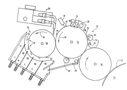
7 Reference is now made to Fig. 1 which illustrates a
8 portion of a multicolor electrostatic imaging system
9 constructed a:nd operative in accordance with a preferred
embodiment of the present invention. As seen in Fig. 1 there
11 is provided ;an image bearing photoconductor surface 12
12 typically found on a rotating photoconductive drum 10. Drum
13 10 is driven in any appropriate manner (not shown) in the
14 direction of arrow 18 past charging apparatus 14, preferably
a corotron, adapted to charge surface 12 of photoconductive
16 drum 10.
17 An image to be reproduced is focused by imaging
18 apparatus 16 upon charged surface 12 at least partially
19 discharging photoconductive drum 10 in the portions impinged
upon by light 1to form an electrostatic latent image.
21 The electrostatic latent image normally includes image
22 portions at a first electrical potential and background
23 portions at another electrical potential. The present
24 invention is e:~pecially useful where the image portions are
discharged anti the background portions remain at full
26 charge. This type of discharge is referred to herein as
27 "reversal" or "write-black" image formation. '
28 Surface 12 typically comprises an organic
29 photoconductor such as the Emerald OPC manufactured by IBM,
or other suitable photoconductor. Photoconductor charging
31 apparatus 14 may be any suitable charging apparatus such as
32 is well known in the art. Imaging apparatus 16 may be
33 modulated laser. beam scanning apparatus, an optical focusing
34 device for imaging an original on a drum or other imaging
apparatus such as is known in the art.
36 Also associated with photoconductive drum 10 are a
37 multicolor liquid developer spray assembly 20, a developing
38 assembly 22, color specific cleaning blade assemblies 34,
39 an electrified squeegee 26, and discharge apparatus 28 which
WO 92/14193 2 ~ O O ~ ~ PCT/NL92/00014
- 6 -
1 are operative to develop the latent image to form a
2 developed liquid toner image for transfer to an intermediate
3 transfer member 30.
4 Developing assembly 22 preferably includes a
development roller 38. Development roller 38 is preferably
6 spaced by about 40-150 micrometers from photoconductive drum
7 10 at a development region 44 and is charged to an
8 electrical potential intermediate that of the image and
9 background portions of photoconductive drum 10. Development
roller 38 is thus operative, to apply an electric field in
11 development region 44 to aid development of the latent
12 electrostatic image. In a typical system the background
13 portions are at -900 Volts, the image portions are at -180
14 Volts and the development roller 38 is at -500 volts when a
liquid developer comprising negative toner particles is
16 utilized.
17 Development roller 38 typically rotates, as indicated
18 by arrow 40, in the same sense as drum 10. This rotation
19 provides for the surface of drum 10 and development roller
38 to have oppositely directed velocities at development
21 region 44. The rotation speed of development roller 38 is
22 chosen such that development roller 38 acts inter alia as a
23 metering device. This metering effect ensures that very
24 little liquid carries past development region 44.
Multicolor liquid developer spray assembly 20 provides
26 a spray of liquid toner containing electrically charged
27 pigmented toner particles which can be preferably directed
28 onto a portion of the roller 38 or alternatively onto a
29 portion of photoconductive drum 10 or directly into
development region 44.
31 A preferred toner for use in the present invention is
32 prepared by mixing ten parts of Elvax II 5950T (E.I. du
33 Pont) and five parts of Isopar L (Exxon) at low speed in a
34 jacketed double planetary mixer connected to an oil heating
unit set at 130°C for one hour. 5 parts of Isopar L are
36 added to the mix and the whole is mixed for a further hour
37 at high speed. Ten parts of Isopar L, preheated to 110°C,
38 are added, and mixing is continued without heating until the
39 temperature of the mixture drops to 40°C. Ninety grams of
CA 02104028 2000-12-22
the resultant product is transferred to a O1 attritor (Union
Process) together with 7.5 g. of Mogul L (Cabot) and 120 g.
Isogar y L. The mixture is ground for 24 hours with water
cooling (~20C). The resultant toner particles have a
median (by weight) diameter of about 2.1 Vim. The resultant
material is diluted to a non-volatile solids content of 1.5%,
using Isopar L and charge director as known in the art is
added to charge the toner particles.
Other appropriate liquid toners may alternatively be
employed. For colored liquid developers, carbon black is
replaced by color pigments as is well known in the art. In
an alternate preferred embodiment of the invention the
latent image is developed using powder toner as is known in
the art.
Color specific cleaning blade assemblies 34 are
operatively associated with development, roller 38 for
separate removal of residual amounts of each colored toner
remaining thereon after development. Each one of blade
assemblies 34 is selectably brought into operative
association with development roller 38 only when toner of a
color corresponding thereto is supplied to development
region 44 by spray assembly 20. The construction and
operation of cleaning blade assembly 34 is more fully
described in PCT International Publication number w0
90/14619;
Each of cleaning blade assemblies 34 includes a
toner directing member 52 which serves to direct the toner
removed by the cleaning blade assemblies 34 fzom the
development roller 38 to respective collecting tanks 54, 56,
58 and 60 and thus to prevent contamination of the various
developers by mixing of the colors. The toner thus collected
is recycled to corresponding toner reservoirs (not shown)
for reuse. A final toner collection member 62 always engages
the development roller 38 and the toner collected thereby is
supplied to a clear liquid reservoir (not shown) via a
collecting tanY 64 and a separator (not shown) Which is
operative to separate relatively clean carrier liquid from
the various colored toner particles. The separator may be
CA 02104028 2000-12-22
- 8 -
typically of the type described in PCT International
Publication Number W090/10896
An electrically biased squeegee roller 26 such as that
described in U.S. Patent 4,286,035
is preferably urged
against the surface of drum 10 and is operative to remove
substantially all of the liquid carrier from the background
portions and to compact the image and remove liquid carrier
- l0 therefrom in the image portions. Squeegee roller 26 is
preferably formed of resilient slightly conductive polymeric
material, and is charged to a potential of several hundred
to a few thousand volts with a polarity such that an
electric field is created between squeegee roller 26 and
drum 10 which drives the charged toner particles toward drum
10. Squeegee roller 26 is also operative to further charge
the toner particles and photoconductor surface 12 as
described below.
Transfer of the developed image to an intermediate
transfer member 30 (or to a final substrate) from drum 10
generally requires the imposition of an electric field
between drum 10 and the surface of intermediate transfer
member 30. It has beQn found that if a potential sufficient
to effect substantially complete transfer of the developed
image is impressed on intermediate transfer member 30, then
a high potential difference is established between the
intermediate transfer member and background portions on the
drum 10 causing electrical discharge therebetween.
In a preferred embodiment of the invention, discharge
apparatus 28, which is descried in more detail below, is
operative to irradiate drum 10 with light characterized by a
predetermined intensity and spectrum to reduce electrical
discharge between drum 10 and intermediate transfer member
30.
Intermediate transfer member 30 may be any suitable
intermediate transfer member as is known in the art such as
those described ~ ~?GT .atonal Publication Wo
90/08984
and is maintained at a volta~ -w temperature
WO 92/14193 ~ o ~ g PCT/NL92/00014
- g -
1 suitable for electrostatic transfer of the image thereto
2 from drum l0 and therefrom to a final substrate 72 such as
3 paper.
4 Intermediate transfer member 30 is preferably
associated wii:h a pressure roller 71 for transfer of the
6 image onto final substrate 72 preferably by heat and
7 pressure. In a preferred embodiment of the invention
8 intermediate transfer member 30 is coated with a non-stick,
9 preferably a silicone, coating to aid in subsequent transfer
of the developEad image therefrom to substrate 72.
11 Cleaning apparatus 32 is operative to clean the
12 photoconductor surface 12 and includes a cleaning roller 74,
13 a sprayer 76 to spray a non polar cleaning liquid to assist
14 in the cleaning process and a wiper blade 78 to complete the
cleaning of surface 12. Cleaning roller 74, which may be
16 formed of an5r synthetic resin known in the art for this
17 purpose, is driven in a direction of rotation indicated by
18 arrow 80 which is the same as the direction of rotation of
19 drum 10.
Any residual charge left on the surface of drum 10 is
21 removed by flooding surface 12 with light from a
22 neutralizing limp assembly 36.
23 In accordance with a preferred embodiment of the
24 invention, after developing each image in a given color, the
single color ~.mage is transferred to intermediate transfer
26 member 30. Subsequent images in different colors are
27 sequentially transferred in alignment with the previous
28 image onto intermediate transfer member 30. When all of the
29 desired images have been transferred thereto, the complete
multi-color image is transferred from transfer member 30 to
31 substrate 72.
32 Alternatively, each single color image is transferred
33 to the substrate directly after its transfer to intermediate
34 transfer member 30. In this case the substrate is fed
through the machine once for each color or is held on
36 pressure roller 71 and contacted with intermediate transfer
37 member 30 during each image transfer operation.
38 Reference is now made to Fig. 2 which illustrates
39 typical post-development electrical potentials (before
~i(1~U28
WO 92/14193 PCT/NL92/00014
- 10 -
1 application of squeegee roller 26) on the surface of drum 10
2 at background portions 110 (~-900 volts) and image portions
3 112 (~-180 volts) and on the surface of the developed image
4 114 (~-450 volts). These potentials are not fixed values but
rather depend on charge on the photoconductor before
6 development, spectrum and intensity of the image projected
7 by imaging apparatus 16, photoconductor response
8 characteristics, process speed, development roller 38
9 potential, the toner charge, mobility and viscosity and
other factors.
11 To assure good transfer of the charged toner particles
12 in the developed image from drum 10 to intermediate transfer
13 member 30 a suitable potential difference must be maintained
14 between the surface of intermediate transfer member 30 and
image portions 112 on the surface of drum 10. The magnitude
16 of this potential difference is dependent on a number of
17 factors such as the type of toner, the toner layer charge
18 and thickness and the relative affinity of the toner for
19 surface 12 and the surface of intermediate transfer member
30. The magnitude of this potential difference is not
21 believed to be a function of the absolute potential on image
22 portions 112, and a range of potential differences, near an
23 optimum potential difference, give good results.
24 It is desirable to reduce the potential difference
between the surface of intermediate transfer member 30 and
26 background portions 110 of surface 12 to reduce electrical
27 discharge therebetween. This electrical discharge is
28 believed to cause deterioration of the non-stick properties
29 of the silicone surface coating of intermediate transfer
member 30 and damage to the photoconductor.
31 It might have been thought that flooding drum 10 with
32 high intensity light would discharge background portions 110
33 and be operative to significantly reduce the discharge. The
34 present inventors have found, however, that light which
penetrates the developed image to image portions 112 which
36 underlie the developed image causes not only a reduction in
37 the potential of image portions 112, as expected, but can
38 actually cause image portions 112 to become positively
39 charged in the presence of the negatively charged toner
WO 92/14193 ~ g PCT/NL92/00014
- 11 -
1 image overlying them. Since the potential of intermediate
2 transfer member 30 must also be adjusted to account for the
3 change in potential of image portions 112, it has been found
4 that the potential difference between background portions
110 and the surface of intermediate transfer member 30 still
6 causes electri~~al discharge.
7 In such a case and in a particular example thereof,
8 without any light treatment but after subjecting the image
9 to squeegee :roller 26, the optimum transfer potential of
intermediate 'transfer member 30 is -400 volts and the
11 potential of background portions 110 is -1220 volts,
12 resulting in .3 820 volt potential difference therebetween.
13 The developed :image is at a potential of -960 volts.
14 After ir~~adiation of drum 10 with strong light, the
potential at i~he developed image falls to -250 volts, and
16 the optimum transfer potential is +400 volts. The background
17 had a potential of about -130 volts resulting in a potential
18 difference bei:ween the background portions of the drum and
19 the intermediate transfer member of 530 volts. At this
potential difference electrical discharge still occurs. It
21 is believed that for even stronger irradiation, the
22 potential difi:erence increases further until a saturation
23 value is reached.
24 As previously noted, discharge apparatus 28, is
operative to irradiate drum 10 with light characterized by a
26 predetermined intensity and spectrum to reduce electrical
27 discharge between drum 10 and the surface of ' intermediate
28 transfer member 30. The present inventors have found that
29 controlled irradiation of drum 10 before transfer of the
developed images therefrom can allow for optimal transfer of
31 the image without electrical discharge between background
32 portions 110 and intermediate transfer member 30. This
33 controlled irradiation is chosen to be strong enough to
34 substantially discharge background portions 110 to a
potential near zero and weak enough so that the attenuated
36 light which passes through the developed image changes the
37 potential of image portions 112 underlying the developed
38 image to a substantially lesser degree.
39 Reference is made to Figs. 3-5 which illustrate the
WO 92/14193 ~ ~ ~ PCT/NL92/00014
- 12 -
1 effect of various amount of light on the various potentials
2 in the system, in accordance with a preferred embodiment of
3 the invention.
4 Curve "A" of Fig. 3 shows the potential on background
portions 110 after illuminating drum 10 with light of
6 varying intensities from a light source comprising a row of
7 miniature incandescent lamps. The light intensity is
8 referenced by the voltage on the light source (i.e. the
9 lamps). Curve "B" shows the potential on background portions
110 which are subjected to squeegee roller 26 electrified to
11 a potential of -2400 volts before they are illuminated.
12 Curve "A" of Fig. 4 shows the potential on the
13 developed image 114 as a function of light source voltage,
14 after subjecting the image to squeegee roller 26 at a
potential of -2400 volts. As used herein the term "developed
16 image" includes an image which may have been subjected to a
17 squeegee roller or to other post-formation treatment, other
18 than irradiation by light. If the squeegee roller is not
19 used, then for zero light intensity, the potential on the
developed image is approximately 500 volts more positive
21 than shown on curve A, i.e., about -450 Volts.
22 It is believed that the potential change caused by the
23 electrified squeegee roller is in part the result of
24 charging of image portions 112 of drum 10 and in part the
result of the addition of further negative charge to the
26 already negatively charged toner particles.
27 It is noted, however, that irradiation by light causes
28 a change only in the potential of image portions 112 and is
29 not believed to be effective in changing the charge on the
toner particles. Thus any change in the image potential of
31 developed image 114 which is caused by light is believed to
32 be caused by changes in the potential of image portions 112.
33 Also plotted in Fig. 4 as curve "B" is the potential on
34 the intermediate transfer member for "optimal" transfer of
the image from the drum to the intermediate transfer member.
36 Curve "A" of Fig. 5 is the potential difference between
37 background portion 110 and the intermediate transfer member
38 30 at the optimal transfer potential as a function of light
39 source voltage (i.e., curve "B" of Fig. 3 minus curve "B" of
WO 92/14193 ~ ~ ~ ~ ~ ~ ~ PCT/NL92/00014
- 13 -
1 Fig. 4). Curare "B" of Fig. 5 is the potential difference
2 between developed image 114 and intermediate transfer member
3 ("ITM") 30 a:a a function of light source voltage (i.e.,
4 curve "A" of F:ig. 4 minus curve "B" of Fig. 4). It should be
noted that the image-ITM potential difference is essentially
6 constant, within the ~50 volt estimated error in measurement
7 of surface potsantial. This constancy of potential difference
8 required for optimal transfer supports the above mentioned
9 premises that i:he potential difference required for transfer
is not a function of the absolute image portion potential
11 and that light does not change the charge of the toner
12 particles.
13 Furthermore the image transfer "quality" does not
14 appear to be a function of the light level. On the other
hand, as the light level is increased the potential
16 difference between the intermediate transfer member 30 and
17 the background portions 110, which starts at a high value,
18 first falls to a minimum value and then rises again as the
19 light level is further increased.
It should be noted that the potential of image portion
21 112 is believed to be several hundred volts lower (i.e.,
22 more positive) than the potential of the image 114 so that
23 the potential difference between image portion 112 and the
24 ITM is believs~d to be in the range of approximately 70-350
volts.
26 For a ~pa,rticular range of light intensities, the
27 potential difference between background portions 110 and the
28 surface of intermediate transfer member 30 is reduced below
29 the minimum F~roducing discharge. As is well known, the
discharge voltage between two flat surfaces has a high value
31 for very small and for very large spacings between the
32 surfaces. For intermediate spacings the discharge voltage
33 reaches a minimum, which for air at standard pressure is
34 approximately 36o volts (at a spacing of approximately 8
micrometers). The curve of discharge voltage as a function
36 of spacing is generally known as the Paschen curve and the
37 minimum voltage is called the "minimum of the Paschen
38 Curve". For flat surfaces, discharge cannot occur if the
39 potential difference between the surfaces is less than the
~I~~~U~~
WO 92/14193 PCT/NL92/00014
- 14 -
1 minimum of the Paschen Curve. While it is especially
2 preferred to utilize a background-ITS voltage lower than
3 this lowest minimum value, it is believed that somewhat
4 higher potential differences, while they may cause some
discharge, do not cause substantial enough discharge to
6 substantially damage the photoconductor or the non-stick
7 coating of the intermediate transfer member.
8 As can be seen from Fig. 5, for the particular case
9 discussed, there is a range of lamp voltages (and
corresponding light intensities), which results in
11 background-ITM potential differences below 360 volts. It is
12 believed that this is a relatively safe value for
13 substantial elimination of discharge. Optimally, the amount
14 of light is adjusted to give a minimum potential difference.
The light source employed in the discharge apparatus 28
16 in the above described experiments is a row of 14 series
17 connected 0.79 watt incandescent lamps (@ 7.86 VAC each),
18 spaced 26 mm apart and spaced 8 mm from the drum. The drum
19 velocity is 60 cm/sec and a black image having a
transmission optical density of approximately 0.7 is used.
21 In a preferred embodiment of the invention light having
22 a color which is complementary to the color of the image on
23 the drum 10 is used to illuminate drum 10. In this case the
24 amount of light transmitted through the image to image
portion 112 is substantially reduced and for a particular
26 light intensity, the background-ITM potential difference may
27 be reduced to a very low value. The source of light may be a
28 series of light emitting diodes which emit colored light
29 complementary to the color of the tower particles in the
image. Alternatively, other sources of colored light such as
31 cold cathode discharge sources can be utilized in the
32 practice of the invention. Alternatively, a source of white
33 light with appropriately colored filters is utilized to
34 produce the complementary colors.
The amplitude of each of the sources is preferably
36 matched to the toner optical density and photoreceptor
37 characteristics by varying the intensity of the white light
38 or by use of neutral density filters.
39 The white light may be from incandescent lamps or may
WO 92/14193 2 ~ p ~ 0 2 8 PCT/NL92/00014
- 15 -
1 be from fluorescent lamps.
2 It should be noted that the lower the transparency of
3 the pigments used (i.e., the higher the density of the image
4 for the given c:olor), the lower the effect on the potential
of the portions of the drum underlying the image. For very
6 dense images, the possibility exists that very low, even
7 zero, potential difference between the surface of the
8 intermediate transfer member and the background portion of
9 drum 10 can be achieved at the optimum transfer voltage.
Under certain circumstances the minimum of the curve of
11 background-ITM potential difference can reverse sign.
12 While the invention has been described utilizing a drum
13 photoconductor, a roller developer, liquid toner and for
14 transfer utilizing an intermediate transfer member, it is
understood tha the invention can be practiced utilizing a
16 belt developer and/or.a belt photoconductor, any appropriate
17 liquid or dry toner as is known in the art and/or direct
18 transfer from drum 10 to substrate 72.
19 Furthermore, while the invention has been described
utilizing a controlled source of light for differentially
21 discharging the image and background portions of the image
22 forming surface, other means for selectively discharging are
23 within the scope of the invention.
24 For a~ positively chargeable photoconductor, using
positive toner particles in a reverse development mode,
26 similar results will be obtained, with only the signs of the
27 potentials reversed.
28 It will b~e appreciated by persons skilled in the art
29 that the present invention is not limited by what has been
particularly shown and described hereinabove. Rather the
31 scope of the present invention is defined only by the claims
32 which follow: