Note: Descriptions are shown in the official language in which they were submitted.
2~0~
,
OPIICAL SiGNA~L IDE:NTIFICATION TEClHNIQUE
Technical Field
The invention relates to the optical ~nsmission of info~mation and, more
particularly, to improving signal demultiplexing within a wavelength-multiplexed optical
S transmission system.
Back~olmd Of The Invention
Within wavelength-multiplexed optical transmission systems several encoded
optical signals (referred to as "channels"), each having a different wavelength, are transmitted
simultaneously along a single optical path (typically an optical fiber). At the receiving end
10 of such a system, the optical signals are separated ("demultiplexed"), and individually decoded.
Previous arrangements for demul iplexing wavelength-multiplexed channels
have employed bandpass opdcal filte~ these arrangements, a number of bandpass filters,
each fixed`at or tuned tO the wavele1lgth of a particular channel, are deployed at the receiving
end of an optical transmission system. 'rO insulate against cross-~lk, and minimize noise, the
15 passband of e~ch of ~hese filters is typically limited to a very narrow window (usually only
a fraction of ~he inter-channel separation).
One of the drawbacks of demultiplexing optical signals using bandpass ~lters
is that the ~ ers, as well as the optical sources producing the multiplexed channels, are subject
to wavelength drif~ng as a function of environmental condi~ions and time. As a result, a
20 mismatch is likely to develop between ~he wavelength of a channel and the passband of the
filter dedicated ~o demultiplexing tha~ si~nal. Given the typically n~ow passbands of the
filters, it is likely dlat any drifting by eithe~ the filters or the optical sou~ces would result in
a demultiplexing failure and the loss of the encoded signal.
llhe above problem of drift can be colsected ~or by condnually monitoring and
25 adjusting the optical sources and receiving ~llters. lEIowever, such correction rneasures prove
expensive as a result of labor costs (if ~hey are manually implemented), or as a result of
increased hardware costs (i they are automatically implemented via ac~ive feedback loops).
In either case, the monit~ring and adjustin~ of the soarces and filters does not offer a practical
`- 2 ~ 9
- 2 -
soludon to the problems associated with wavele~lgth drift within a wavelength-multiplexed
opdcal transmission system.
'rhe present inven~ion overcomes ~e deficiencies of pAor waveleng~h-
S multiplexed optical signal idendfication techniques by moduladng each of the individual
channels within a muldplexed signal at a unique low-frequency. This modulation is perforrned
at the transmission site of the optical signal, and the speci~lc frequencies of modulation a~e
chosen to be very much lower than the low-frequency cut-off of any other inforrnation
encoded upon the optical signals. At the reception site of the multiplexed signal, the invention
directs each of the individual optical signals, as a funcdon of the particular low-frèquency
modulation evident upon each signal, to a particular tunable Fabry-Perot ("FP") optical filter.
As FP filters have the ability to track the frequency of an individual channel, problems
associated with wavelength drift are eliminated. Furthermore, FP filters offer a very na~row
optical passband, allowing inter-channel cross-talk and noise levels to be minimized within
waveleng~h-multiplexed optical systems employing the signal identifica~on technique.
In the drawing:
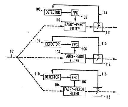
FIG. 1 shows, in simpli~led form, a block diagram of a ~equency-multiplexed
opdcal communicadon system employing the invention;
FIG. 2 shows, in s;mpli~ed form, a schematic diagram of detector circuit 109
of FIG. l;
FIG. 3A provides a graphical illustradon of the signal output from
splitter/sensor 112 of FIG. 1 as FP filter 103 of FIG. 1 is scanned across a band including
wavelengths ~" ~2, and ~;
FIG. 3B provides a graphical illustradon of the signals input to, and out from,
comparator 204 of FIG. 2;
FIG. 3C provides a graphical illus~ration of the signals input to, and out from,comparator 203 of FIG. 2; and
FIG. 3D provides a graphical illus~ration of the signals input to, and out from,flip-flop 206 of FIG. 2.
i . , .
, ~ , ,
., . . - ,,
2~0~L18~
- 3 -
~}~1~ Uf The ~nvention
ln a preferred embodiment of the invention, a wavelength-multiplexed optical
signal, compnsed of three individual optical component signals having wavelengths of ~ 2~
and ;43, is ~ansmitted from a source to a receiver via an opt;cal fiber. E~ach of these individual
component signals, within the wavelength-multiplexed optical signal, is amplitude modulated
at a unique low-frequency -- fl, f2, and f3, respectively. This low-frequency amplitude
modulation is independent of, and in addition to, any other modulation of the optical signals
(such as high-frequency digital or analog inforrnation encoding). Any one of a number of
well-known techniques for amplitude modulating an optical signal may be employed to effect
the low-frequency moduladon of the individual component opdcal signals. One suchtechnique employs alternating waveforms of frequencies fl. f2, and f3 to modulate the bias
cunrent of each of the lasers producing the individual optical signals. While the specific low-
frequency modulation technique is imrnaterial, the modulation frequencies must be very much
lower than the low-frequency cut-off of any receiver coupled to the optical ~lber for purposes
o~ decoding high-freguency digital or analog information. This ensures that the reception of
any high-frequency information carried by the opdcal component signals will not be interfered
wi~h as a result of the low-f~equency modulation.
FIG. 1 shows a simplified block diagram of a receiver which employs the
invention to demultiplex a wavelength-multiplexed optical signal, in which each of the
individual optical signals are low-frequency modulated as described above. The pathways
illus~rated as dotted Lines in FIG. 1 calTy optical signals, and the pathways illustrated as solid
lines ca~Ty electrical signals. In operation, the wavelength-multiplexed optical signal traveling
along optical fibel 101 is split, and input to three independently tunable FP filters ~102, 103,
and 104~. Each FP filter is scanned over range of wavelengths, including ~, ~, and A3. This
scanning is accomplished via associated PP ISlter controllers ("~PCs"), labeled as 105, 106,
and 107 in lFIG. 1. The optical output of the tunable FP filters fluctuate as the passband of
each FP filter is scanned ove~ the range of wavelengths, wi~ each optical output pealdng as
the passband of a given lE~P filter is tuned to the ~undamental wavelength of any one ~he ~ree
component signals of the input optical signal. Optical splitter/sensors 111, 112, and 113 are
shown to be coupled to the output OI each FP filter. These spliuer/senso~s each produce an
electrical signal proportional to the optical output of an associated FP filter. These electrical
signals are each transmitted (via lines 114, l lS, and 116) to a de~ector circuit (108, 109, and
110). Each of these detector circuits serves to d tect a particular one of the ~hree componen~
2 ~ 9
- 4 -
optic~l signals, and cause the associated FPC and FP filter to phase-lock onto ~hat op~ical
signal.
F~G. 2 shows, in simplified form, a schematic diagram of detec~or circuit 109
(see FIG. 1). The circuit detects the presence of one particular multiplexed optical signal
S which is modulated at the specific low-frequency f2. and enables FP filter 103 to phase-loelc
onto the optical component signal having the ~undamental wavelength of A2. As is shown, the
circuit of FIG. 2 includes bandpass filter 201, amplifier 202, comparators 203 and 204, buffer
205, and flip-flop 206.
1 he posidve input of comparator 204 receives an electrical signal from line 115.
This signal is proportional to the optical ou~tput of ~P filter 103 (PIG. 1). ~he outpu~ of
comparator 204 at~ains a positive value when the amplitude of the signal upon line 115
exceeds that of reference voltage VRI. The value of VRI is fixed at a level which allows the
output of comparator 203 to attain a positive value whenever the elec~rical input signal upon
line 11~ increases in response to the FP filter 103 (FIG. 1) peaking as FP filter 103 is scanned
across wavelengths ~ , and ~3. Wavefonn 301 of FIG. 3A provides a graphical illustration
(amplitude versus dme) o~ the signal which would be evident upon line 115 if FP filter 103
a~IG. 1) were freely scanned across a band including wavelengths ~ 2, and ~. During the
scan, FP filter 103 is tuned to wavelength ~1 at t~, to wavelength ~ at t2, and to wavelength
~3 at t3. FW. 3B pro~ides a graphical illustration (amplitude versus time) of the signal upon
line 115 (wa~eform 302), the output of comparator 204 (waveform 303), and ~e level of
re~erence voltage ~Rl. when FP ~llter 103 (FIG. 1) is phase-locked to the optical component
signal having a gundamental waveleng~h of ~ (as it would in the normal practice of the
invention). For purposes of illustration, the wavefonns in FIG. 3B have not been drawn to
the same scale. Note ~at ~e outpus oP comparator 204 is a ITL signal on the order of 4 to
2S 5 volts, while the level of VRI is typically no more than seveTal hundred millivolts. The
process by which dlis phase-locking is accomplished is discussed below.
The signal evident upon line 115 is also D put to bandpass ~llter 201. Bandpass
filter 201 is adapted to pass electrical signals having a ~requency of f2 to amplifier 202. The
amplified bandpass ffltered signal output from amplifier 202 is then fed to the positive input
of comparator 203. The output of comparator 203 ~ttains a positive value when the amplitude
of ~he input bandpass filtered signal exceeds that of reference voltage VR2. The value of VR2
is fixed at sufficiendy high level to cause ~e output of comparator 203 to attain a positive
value only when a signal ha~/ing a fundamental fieqllency of f2 iS being passed by filter 201.
FIG. 3C provides a graphical illustration ~amplitude versus time) of the signal output by
.
.^,
, , ~
~... ~ , .
2 ~ 8 ~
- 5 -
bandpass filter 201 (waveform 304), the output of comparator 203 (waveform 305), and the
level of referenco voltage VR~ and as FP filter 103 (FIG. 1) is scanned and phase-locked. As
with FIG. 3B, the waveforms in PIG. 3C are not drawn to the same scale. The output of
comparator 203 is a lTL signal on the order of 4 tO 5 volts, while ~e level of Vl,2 is typically
S no more than several hundred millivolts.
As shown in FIG. 2, the output of comparator 203 is fed to the data input of
flip-flop 206, and to buffer 205. The signal from comparator 203 e~ident at the flip-flop data
input serves to ~igger the flip-flop, while the delayed pulse p~ovided by buffer 205 serves as
clock signal, thereby ensuring a stable transition by flip-flop 206. FIG. 3D provides a
graphical illustratioal (asnplitude versus time) of the si,gnal 306 which is output by flip-flop
206. This output is fed to FPC 106 ~FIG. 1).
In response to receiving the output pulse from flip-flop 206 (FIG. 2), FPC 106
(FIG. 1) halts the wavelength scanning of FP filter 103, and places that FP filter ihltO a phase-
lock mode. Since detector circuit 109 ensures ~hat the pulse ou~:put by flip-flop 206 coincides
with passband of FP filter 103 being centered upon ~, ~P filter 103 is locked onto the optical
component signal having a wavelength of ~2.
Detector circuits 108 and 110 (FIG. 1) have configurations similar to that of
detector circuit 109. EIowever, ~e bandpass filter within detector circuit 108 i5 tuned to the
frequency fl. and the bandpass ~llter within detector circuit 110 is tuned to the frequency f3.
As a result, FPC lOS places FP filter 102 into a phase-loc~ mode when the passband of FP
filter 102 is cenle~d upon ~ (as ~he component optical signal of waYelength ~ is modulated
at frequency fl). Similarly, FPC 107 places FP filter 104 into a phase-lock mode when the
passband of FP filte~ 104 is centered upO~I A3 (as the componen~ optical signal of wavelength
~ is modula~ed at frequency f3).
- 25 It will be understood ~hat the particular embodiments described above are only
illustrative of the principles sf the present invention, and that va~ious modifica~ions could ~e
made by those skilled in the art without depar~ng ~om the scope and spirit of the present
invention, which is limited only by the claims that ~ollow.
.~. ~,: . ., , ~
.