Note: Descriptions are shown in the official language in which they were submitted.
~93/t457S 2la~ 7 Pcr/US93/000
MU~TI-ZONE AUDIO D~STR:CBUTION A~lP~IFIER
Field of The Invention
The present invention relates generally to audio
distribution systems and, more particularly, to audio
distribution system amplifier arrangements.
Background O~ The Invention ¦ `
Home owners are rapidly becoming aware of the
benefits of home audio distribution systems. These
benefits include convenient access to audio signals
throughout the home, more efficient use of space, and
savings in the form of reduced equipment need due to
better utilization of existing equipment.
Audio distribution systems range from those
distributing mono signals only, such as doorbell and ;
intercom signals, to those incorporating a selective
mixture of stereo signals and cuch mono signals. Certain
of these systems utilize a switching matrix to distribute
various input signals to various rooms throughout the
house. Speakers in the various rooms typically receive
the amplified signal through a distribution panel located
in the room.
Other prior art systems require purchase of a
separate amplifier unit to distribute each type of
signal.
Another type of audio distribution system includes
multiple level-adjustable mono amplifiers in a single
enclosure, with the multiple amplifiers providing
' -
.. , . . . ~ .. . , . . ., ~ . . ,
W093~4~ 7 PCT/USg3/00090~
parallel mono channels to serve di~ferent types of input
signals. This type of system requires that the system
enclosure be diassembled in order to expand the system
with additional amplifiers.
These types of prior art systems, unfortunately, have
several setbacks. Prior art systems using a switching
matrix to distribute various input signals are unable to
accommodate significant differences in input level
between the various input signals. With respect to those
systems requiring separate amplifier units, space
requirements and cost make it burdensome for users to add
audio components which also require amplification by the
system. Systems using multiple level-adjustable mono
amplifiers in a single enclosure are expensive because
they do not provide user-friendly modularity, they are
unable to serve a wide range of signal types, and their
input level adjustability range is unduly limited.
Accordingly, there is a need for an improved audio
distribution system that overcomes the aforementioned
shortcomings.
8ummary Of The Invention
It is a general object of the present invention to
provide a multi-zone audio distribution system, which is
able to separately amplify mono and stereo signals in a
space-effective and cost-effective manner.
It is another important object of the present
invention to provide a multi-zone modular audio
distribution system that includes multiple level-
93~l4~75 Z~ ~ 9 ~ PCT/US93/~090
adjustable stereo amplifiers arranged in parallPl toserve dif~erent types of audio input signals.
It is yet another important object of the present
invention to provide a multi-zone modular audio
distribution system that includes multiple level~
adjustable stereo amplifiers, each having circuitry for `~
cascading the various amplifiers.
In a preferred embodiment, these and other ob~ects of
the present invention are realized using an audio
lo distribution amplifier system, which includes a housing
having a first side and a second side, a plurality of
amplifier units, and an interface board including edge-
connector means for providing power to each of the
plurality of amplifier units. Each amplifier unit
includes an input port for receiving an input stereo
signal, at least one amplification circuit which
amplifies the input stereo signal, an output port for
providing access to the input stereo signal amplified by
a preselected amplification factor, a printed circuit
board having a face upon which the amplification circuit
is mounted and having interface and side edges, and a
port panel that is connected to the printed circuit board
and that is secured within the housing and adjacent its
second side. The amplifier units are modularly adaptable
to the system such that each amplifier unit is operable
independent of each other amplifier unit and is
accessible via the second side at a position which
receives the port panel.
~:: , " '
W093/l4575 ~ i 0~ 7 PCT/U593/~90
Preferably, the system includes printed circuit board
guides for guiding each of the ampli~ier units along the
side edges to mate with the interface board, and each
amplifier unit further includes a loop-back port for
cascading at least two of the amplifier units. The
amplification circuit may include a heat sink thermally
coupled thereto and a polyswitch arranged as a thermal
shut-back device for interrupting power to the
amplification circuit under undesired thermal conditions.
~rief Description Of The Drawing~
Other objects and advantages of the invention will
become apparent upon reading the following~ detailed
15 description and upon reference to the drawings in which: ~,
Fig. la is a perspective diagram of a multi-zone
audio distribution amplifier system within an exemplary
enclosure, according to the present invention;
Fig. lb is an illustration of the multi-zone audio
distribution amplifier system of Fig. la from the rear
side;
Fig. lc is an expanded illustration of one of several
back panels shown in Fig. lb;
Fig. 2 is perspective diagram of a modular amplifier
card (with attached back panel), which inserts into the
rear side of the enclosure shown in Fig. la;
::
Fig. 3 is a circuit diagram illustrating a preferred
implementation of one of the amplifier circuits
represented by the amplifier card of Fig. 2;
2 1 0 /1 .~ ~ 7 PC~/U593/OUO9~ 1
Fig. ~ is a diagram of an interface board, according
to the present invention, into which each one of the
amplifier circuits of Fig. 2 connects; and
; Fig. 5 is a circuit diagram, also in accordance with
the present invention, of one of the displays shown in
Fig. la.
While the in~ention is susceptible to various
modifications and alternative forms, a specific
embodiment thereof have been shown by way of example in
lo the drawings and will be described in detail. It should
be understood, however, that the illustrated embodiment
is not intended to limit the invention to the particular
form described. On the contrary, the intention is to
cover all modifications, equivalents, and alternatives
falling within the spirit and scope of the invention as
defined by the appended claims.
,)
Description Of The Preferred Embodiment
The present invention is directed to the
, 20 implementation of multiple modularly cascadable
amplifiers in a single conventionally sized (or racked)
unit. The intended applications include a wide variety
of industrial, commercial and consumer uses. For
instance, the present invention is ideally suited for
consumer applications which require amplification of
, ~ different types of audio signals (e.g., stereo from the
television and from the radio, door bell, intercom, etc.)
at a central location. Other features such as
cascadability of the amplifiers and modularity (both of
:: :
.~ '. ' .' ' ' ' , ' ' `' ' ' _ '
wO 93/l4575 2 1 ~ '~ 3 '~ 7 PCltUS93/00090 ~
which will be discussed herein) offer a range of uses not
heretofore known. ~-~
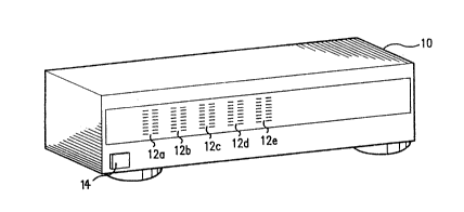
Fig. la illustrates the present invention, as
enclosed in a housing 10 with the front side of the
5 housing showing five pairs OI LED (light emitting diode)
bar graphs 12a, 12b, 12c, 12d and 12e. An on/off switch
14 is shown in the lower left corner of the front side. -
The rear side of the housing is shown in Fig. lb as
' having five identical modular back panels 16a, 16b, 16c,
16d and 16e, one for each respective bar graph pair 12a-
12e, and a power supply panel 18.
The modularity of the system is highly advantageous
from both cost and convenience perspectives. With
respect to cost, the "growability" of the system permits
15 its user to purchase the system with a single amplifier
card at a substantially reduced cost, and later purchase
one or more additional cards for further amplification
requirements as the desired audio uses grow and/or
change. From a convenience perspective, the system is
20 designed to allow its user to remove and insert
individual amplifier cards via access of only two screws,
which are located at the back of the housing for each
back plane (see screw holes l9a and l9b of Fig. lc).
In Fig. lc, each back panel 16 is illustrated as
25 including left and right input ports 18a and 18b, and
~;~ input level-adjust controls 20a and 20b for the
respective left and right input channels.
As an output, the back panel 16 includes a pair of
ports for each of the left and right channels. For the
. .
~? 93~14575 2 t ~ PCT/US93/00090
;~ 7
left output channel, negative and positive ports are
depicted as 22a and 22b: and for the right output
channel, negative and positive ports are depicted as 24a
and 24b.
Another important aspect of the present invention
involves a pair of loop output ports 26a and 26b of Fig.
lc. These ports provide the user with the capability of
cascading the amplifier blocks associated with each
modular back panel 16. For example, in a system using
only four of the five modular positions, one of the
positions may be used in a dedicated manner to amplify a
separate audio signal, while the remaining three
positions may be used in a cascaded manner to amplify
another audio signal three times (once at each position).
In applications requiring amplification of relatively low
signal levels, this feature alleviates the need for a
custom-designed amplification circuit and, in combination
with the input level-adjust controls 20a and 20b,
provides the user with wide-range and narrow-range
amplification control.
Fig. 2 illustrates the back panel 16 connected to an
amplifier card 30. The amplifier card 30 includes a ;
printed circuit board 32, with various amplifier
components 34 thereon, and an air-cooled finned heat sink
36 attached to the circuit board 32 via bolts 38. The
heat sink 36 is used to dissipate heat from the amplifier
chip, discussed infra in connection with Fig. 3.
Also shown in Fig. 2 is one of two conventional
printed circuit board guides which are used to slidably
,
.. , ~ , . . ~ , , ~ ,
Wog3/l457~ 7 i0 ~ 9Ç7 PCT/US~3/OOn~
guide the amplifier card 30 into one of the female
receptacles 40a-40e of the ~nterface board 42 of ~ig. 4.
One of the amplifier cards is added to the system by
first removing a dummy back panel (not shown) from the
rear side of the housing, and then sliding an amplifier
card along the guides into the associated female
receptacle (40a-40e). The back panel 16 is secured to
the printed circuit board 32 via conventional printed
circuit board mounting brackets (attached via screw holes
10 19a and l9b). The final step is securing the back panel ~-
16 to the housing 20 using screws which are inserted
through holes 21a and 21b in the back panel 16.
A preferred implementation of each identical
amplifier circuit 50 is shown in Fig. 3. The circuit of
Fig. 3 includes left and right inputs L and R, anc
corresponding outputs Lo and Ro, respectively. The input
and output circuitry is coupled to left and right
operational amplifiers 52 and 54. The loop-back ports of
Fig. lb are connected to the inputs of the circuit 50. `
Because of the similarity of the input and output
circuitry coupled to each of the amplifiers 52 and 54,
only the input and output circuitry coupled to the left
amplifier 52 will be discussed.
Beginning at the left side of the schematic, the
left-channel input signal is fed through an input level-
adjust potentiometer 56 and divider resistor 58. The
input level-adjust potentiometer 56 is user-controlled by
the level-adjust control 20a of Fig. lc. Capacitors 60
and 62 and resistor 64 provide proper AC coupling to the
:
~ 93/14s7s 2 1 0 ~ ~ ~ 7 PCT/US93/00090
amplifier 52. Th~ output of the amplifier 52 is
connected to a short circuit protection circuit r which
includes an (amplifier) output protection resistor 70 in
series with the parallel combination of polyswitch 66 and
5 resistor 68. The Lo output signal is taken from the ~ ~.
right side of the output protection resistor 70.
The factor of amplification provided by the amplifier :
52 is determined by the value of the feedback resistor :~
72. The other circuitry surrounding the feedback :`
resistor 72 is provided for the internal requirements of
the Sanyo STK4192 chip, which is preferably used to
implement the amplifiers 52 and 54.
The AC power to the circuit 50 is provided from a .
power transformer (not shown) via the circuitry 74 in
dotted lines.
For further in~ormation concerning the theory of
; operation of this circuitry, reference should be made to
the Sanyo data book for part number STK4192.
one aspect of this circuit that is not referred to in
20 the above-referenced data book is the thermal protection :~
circuit surrounding polyswitches 78 and 80. Each of
these polyswitches is used to provide the function of a
crowbar circuit to interrupt power to the amplifiers 52
:: and 54 in the event that the ambient temperature exceeds
: 25 specification. In a preferred embodiment in which
thermal shutdown is provided at 150 degrees Fahrenheit,
+Vcc is 33 Vdc, -Vcc is -33 Vdc, resistor 82 is 100 Ohms,
capacitor 84 is 100 microfarads, capacitor 86 is 10 .
~: microfarads, and the polyswitches 78 and 80 are
.... : .,. - . . .. - .. ... . . ..... ..... .
2 10~9~7 : ~
wos3/l4~7s ~ PCT/US93/00090
implemented using Polly Switch PTC resistor type parts
(a~ailable from Raytheon).
The remaining component values used ~or ~he circuit
50 are listed below. The prefixes "R" and l'cll are used
5 to identify the respective resistors and capacitors j
depicted in the illustrated schematic. These component
values are as follows (in Ohms and farads): ¦
R56 = 100 k R58 = lo k I -
C60 = 2.2 micro C6~ = 470 pico
lo R64 = 49.9 k R68 = lk
R70 = 0.22 R72 = 49.9 k
R82 = loo C84 = 100 micro
C86 = 10 micro R88 = 499
C90 = 100 micro R92 = 3.3 ~ (1/2 Watt)
C94 = 10 micro C96 = 47 micro
R98 = 1 k (1/2 Watt) R99 = 3.3 k (1/2 Watt)
R100 = 1 k (1/2 Watt) C102 = 47 micro
R104 = 3.3 k (1/2 Watt) R106 = 3.3 k (1/2 Watt)
R108 = 49.9 k C110 = 100 micro
R112 = 499 R114 = 100 k
R116 = 10 k C118 = 47 micro
R120 = 4.7 k C122 = 47 micro
R124 = 1 k (1/2 Watt)
Referring now to the interface board 42 of Fig. 4, in
2S addition to the female receptacles 40a-40e, the interface
board 42 carries conventional circuitry 130 for the led
bar graphs and carries power from the power supply module
to each of the amplifier boards. Power is provided via ~
printed circuits on the mother board from the power ;;
supply module to each of the female receptacles 40a-40e.
This power includes each of the Vcc, ground and AC ;
signals illustrated and discussed in connection with Fig.
3.
Fig. 5 illustrates the led bar graph circuitry 130,
which includes an LM3915N type display driver 132 and an
LTAlOOOR type led bar graph display 134. The input
signal to the bar graph is taken from the respective left ~;
:~ :
2t ~ L~'( 9 l~ 7
3/~4~75 11 PCT/US93/00090
channel or right channel input of the circuit of Fig. 3,
via a lo kOhm resistor (not shown).
Accordingly, the present invention provides a cost-
effective and user-friendly modular amplifier system for
a multi-zone audio distribution application. While the
inventive system has been particularly shown and
described with reference to certain embodiments, it will
be recognized by those skilled in the art that
modifications and changes may be made to the present
invention described above without departing from the
spirit and scope thereof.
:~. . ; : ... ; . ; . . .. . :::; : . :: .~ .
. . - :. .