Note: Descriptions are shown in the official language in which they were submitted.
W~93/14519PCT/US92/10858
GTO module wlth stacked bypass diode
2 1 0~71
Backarou~d of the Invention
Field of the Invention
The present invention relates to mounting arrange~ents
~or high voltage/high power semiconductors, and in particular
~or GT0 thyristors with bypass diodes.
~escri~tion of the Re1ated Art
Traction vehicles such as rail transit vehicles are
~requently powered by either direct current (DC) or --
alternating current ~AC) electr~c motors. The power developed
by such motors may be as high as lO00 horsepower (HP) per
motor. Such high HP motors require commensurately high,
controlled electric power. For example, a nominal power
requirement may be 750 volts at lO00 amperes when the motor is
operated in a propulsion mode. The motors also typically are
used for electrical braking of the traction vehicle by
operating them as generators, which may produce even higher
voltages and currents. In the case of an AC electric motor
operatlng as a generator, the peak voltage routinely exceeds
lO00 volts.
Power control systems for such ele¢tric traction ~otors
typically use power semiconductor device5, such as gate turn
o~f ~GTO) thyr~stors, to control power flow to and from the
motors. Due to the magnitude of the power being controlled,
there is a significant amount of heat that must be dissipated
by the semiconductor devices. This heat is generally
dissipated by mounting the semiconductors on relatively large
heat sinks. The heat sinks are metal conductors having good
thermal characteristics and sufficient surface area to
dissipate sufficient heat to maintain the semiconductors
within their operating temperature limits.
The semiconductors are connected to high potentials. For
many applications, it is desirable for safety reasons that
such large heat sinks be maintained at electrical ground
potential. Thus, some form of electrical insulation may be
provided between the semiconductors and the heat sinks.
However, any such electrical insulation must be a good thermal
, . .. . . . .. . ...... . . . . .. .
: . .. ... . - " , . , ~ ,
.. . .
Wos3/14519 PCT/US92/10858
conductor, sl~ncQ l~ is positioned between the semiconductors
and the heat sink. The insulation conventionally used is a
sheet material available under the trade name of~Chotherm,
which is believed to be a boron nitride material with a
silicon binder. In a conventional application, each
semiconductor is clamped to the heat sink, with the Chotherm
sheet clamped therebetween
The AC traction drive power supply commonly used in
transit vehicles is a voltage source pulse w~dth modulated GT0
thyristor inverter. The switching is done by the GTo
thyristor, but a bypass diode is placed in antiparallel across
the GT0 thyristor due to the inductive nature of the traction
motor load. A snubber diode and snubber capacitor also are
normally needed to limit voltage during turn off. Finally, a -
lS remotely located res-stor normally is connected to dissipate
the energy trapped in the capacitor.
Semiconductors of this power requirement are preferably
packaged in "press packs" in which the cathode and anode
terminals are large flat sur~aces on opposite ends of the
semiconductors. The GT0 thyristor and diode commonly are
mounted to the heat sink side by 5ide using separate clamps.
This side by s~de ~ounting o~ the already large press pa¢ks
reguires a large heat ~ink and a large area o~ insulating
material.
Summarv of the Invention
It is the object o~ the present invention to provide a
mounting arrangement ~or a GT0 thyristor and its bypass diode
which minimizes the surface area of the insulating material
required, reduces the size of the heat sink reguired, reduces
the number of clamps reguired and provides a highly compact
total package.
These objects are achieved according to the present
invention by piggybacking the bypass diode on top of the GT0
thyristor, rather than mounting them to the heat sink side by
side. Thick bus plates on the top o~ the bypass diode and
bottom of the GT0 thyristor simultaneously serve as electrical
connections and local thermal storage. If desired, a bus
`.' ' ' ~ . : , '.' - ' , !
WO93/14519 ~ 7 ~ PCT/US92t10858
plate between the bypass diode and the GTo thyristor also can
be thickened to act as additional local thermal storage.
The present invention recognizes that the bypass diode
dissipates only a fraction of the power of the GT0 thyristor, -
and that the bypass diode can operate at higher temperatures
than the GT0 thyristor. Thus, the bypass diode does not need
as e~fective a connection with the heat sinks as the GT0
thyristor.
The present invention also recognizes that the power
supply mounting structure used in transit vehicles can benefit
from the nature o~ the transit vehicle's duty cycle operation.
It is common for the peak rate of power dissipation in a GTO
thyristor used in a transit application to be more than five
times the average rate of power dissipation, with a typical
duty cycle repeating every one to two minutes. Thus, by
providing local thermal storage, the present `invention allows
the heat sinks for the entire power supply pac~age to be sized
to dissipate heat at only the average rate, which is
substantially smaller than what would be necessary to
dissipate the peak load.
If needed for a particular application, the conventional
layer of electrically in5ulating, thermally conducting
material still can be po51tioned between the bottom bu~ plate
and the heat sink, but it can be much smaller, since it now
need only insUlate the GTO thyristor, not both the GTO
thyristor and the bypass diode. In addition, the piggybacked
GTO thyristor and bypass diode can be mounted to the heat sink
with a single clamp, instead of the two clamps conventionally
re~uired for side by side mounting.
If desired, the snubber diode also can be stacked with
the other components, since they are even less sensitive to
temperature than the bypass diode.
Brief Description of the Drawinas
The invention will be described in greater detail with
3 reference to the drawings, in which:
. ,
WO 93/14519 211) ~ ~ 71 PCI/US92/10838
Fig. 1 is a plan view of a side mounting panel of a power
supply and support structure according to the present -~
invention.
Fig. 2 is a view along line 2-2 in Fig. 1 with the side
sheet removed.
Fig. 3 is a view along line 3-3 in Fig. 1.
Fig. 4 is a conceptual view o~ th¢ layout and electrical
connections of the components shown in Fig. 1.
Figs. 5 and 6 are alternative electrical schematics for a
power supply according to the present invention.
Detailed Descri~tion of the Preferred Embodiments
A power supply 10 best seen in Figs. 2 and 3 is mounted
to a support panel 12, which is best seen in Fig. 1. The
support panel 12 is provided with bolt holes, flanges or other
mechanisms for mounting the entire power supply 10 in a
suitable location, e.g., a transit vehicle.
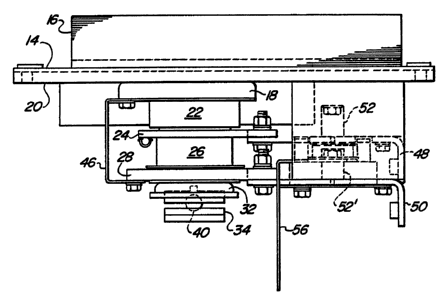
A heat sink 14 having a plurality of heat dissipation -
fins 16 is held spaced from the support panel 12 by suitable
support brackets 17. A substantially flat first bus plate 18
20 i8 positioned next to and is thermally connected to the heat
~ink 14. The first bus plate 18 can rest dire¢tly against the
heat slnk 14, but preferably ls separated from it by a sheet
20 of thermally conducting, but electrically insulating
material, e.g., Chotherm, to keep the heat sink 14 from being
raised to a high voltage.
A press pack-type gate turn off (GTOJ thyristor 22 rests
against the ~irst bus plate 18, with the anode of the GTO
thyristor 22 electrically connéctéd to the first bus plate 18.
The first bus plate 18 preferably has a larger surface area
than the GTO thyristor 22 to spread out the heat flow to the
heat sink 14. This simultaneously allows the heat sink 14 to
operate more efficiently and minimizes the likelihood of
electrical channeling through the sheet insulation 20 at hot
spots.
A substantially flat second bus plate 24 rests against
the GTO thyristor 22, with the cathode of the GT0 thyristor 22
electrically connected to the second bus plate 24. A press
~ ~ , ~ . .. .. ..
WO93/1~519 ~ 9 7 1 PCT/US92/10858
pack-type bypass diode 26 rests against the second bus plate
24, with the anode of the bypass diode 26 electrically
connected to the second bus piate 24. A substantially flat
third ~us plate 28 rests against the ~ypass diode 26, with the
cathode of the bypass diode 26 electrically connected to the
third bus plate 28.
A clamp shown generally at 30 holds the stac~ made up of
the ~irst bus plate 18, insulating sheet 20 (if any), GT0
thyristor 22, second bus plate 24, bypass diode 26 and third
bus plate 28 against the heat sink 24. Any suitable clamp may
be used for this purpose.
~ he clamp 30 shown in Fig. 3 has a plastic insulator 32
which is pressed against the third bus plate 28 by a
compression spring 34. The other side of the spring 34 is
held in place by nuts 36 on bolts 38 which are mounted in the
heat sink 14. A suitable depression or other mechanism
preferably is provided to ensure centering of the plastic
insulator relative to the press-packs. Similarly, the plastic
insulator 32 preferably is provided with a centering ball 40
to center it relative to the spring 34.
As shown in Fig. 2, a strap 46 electrically connects the
~ir~t and third bus plateg 18, 28. The second and third bus
plates 24, 28 algo are connected to extension plates 48, 50,
respectively, to provide electrical connections outside of the
power supply lO. In use, one o~ the extension plates 48, 50
would be connected to an AC line in, and one to a DC line out.
Which is which depends on the wiring configuration ~discussed
below).
Either a snubber diode S2 is mounted to extension plate
48 with its anode electrically connected to the extension
plate 48, or a snubber diode 52' is mounted to extension plate
50 with its cathode electrically connected to ex*ension plate
50, depending on the wiring configuration (discussed below).
As best seen in Fig. 3, a snubber capacitor 54 is mounted
between the clamp 30 and the support panel 12. It may be held
in place by any suitable means, e.g., a bracket 56. Its
terminals are electrically connected between the DC line out
~. ~ . . . . . . .
WO93/14519 2 ~ o ~ ~ r~ 1 PCI/US92/108~8
and the cathode of s~ubber diode 52 or the anode of snubber
diode 52~. -
A suitable control mechanism 58 for controlling the GTo
thyristor 22 preferably is mounted as part of the power supply
10. Such control mechanisms are~ known in the art and will not
be described further here.
The various bus plates 18, 24, 28 preferably are in
thermal contact with the ad~acent GT0 thyristor 22 and bypass
diode 26, and are sized and of a material such that they act
as local thermal storage. The bus plates 18, 24, 28 then can -
store heat when the power supply is under peak power demands,
the dissipate it to the heat sink 14 at an average rate.
If sufficient local thermal storage is provided, the
heat sink 14 can be sized to dissipate only the heat generated
15 on average over the duty cycle of the power supply 10, rather -
than the heat generated at peak power. This means the heat
sink 14 can be considerably smaller than in a conventional
structure.
In a typical transit application, the duty cycle is on
the order of a minute or two. The commercially available GT0
thyristor~ o~ this capacity generally have a thermal time
¢onstant o~ a ~ew seconds. Sizing the bus plates 80 that they
will provide loGal thermal storage with à thermal time
constant on the order of a few tens of seconds should allow
the heat sink 14 to be sized for just the average heat
dissipation requirements of the power supply 10. Thick copper
plates can meet these reguirements in a typical applications.
Fig. 4 shows a conceptual view of the relative positions
and wiring connections of the components just described, in -
the embodiment with the cathode of snubber diode 52' connected
to extension plate 48, and the snubber capacitor 54 connected
between the anode of snubber diode 52' and extension plate 50.
In this embodiment, extension plate 48 would be connected to
AC line in, and extension plate 50 would be connected to DC
line out.
In the alternative embodiment mentioned above (but not
shown in Fig. 4), the anode of snubber diode 52 would be
; ~;.,~ ~: , ~ ....... - . - -
. " ,,
: ........... , . . , - .......... .. : -, . .
::. . . . . . , .: ,: . .
:: , , - : . ,
. .: . . . ..
WO93/14519 ~ 7 1 PCT~US92/10858
connected to extension plate 50 and the snubber capacitor s4
would be connected between the cathode of snubber diode 52 and
extension plate 48. Extension plate 48 would be connected to
DC line out, and extension plate 50 to AC line in.
This conceptual representation also shows a drain
resistor 60 connected between ground and the terminal of the
snubber capacitor 54 which is also connected to the snubber
diode 52 or 52' to dissipate the energy trapped in the snubber
capacitor 54. Such a resistor 60 typically is located
remotely from the power supply lO.
Figs. 5 and 6 show the alternative wiring connections
just described in their most basic schematic forms (with the
control mechanism 58 for the GT0 thyristor 22 omitted). In a
normal application, a transit vehicle would be provided with
two power supplies lO, one wired as shown in each of Figs. S
and 6, to capture power in both halves of the AC power cycle.
While the invention has been described in conjunction
with a speci~ic embodiment, it is to be understood that many
alternatives, modifications and variations will be apparent to
*hose ~killed in the art ~n light o~ the foregoing
description, Ac¢ordingly, this invention i6 intended to
embrace all such alternatives, modi~ications and variations
which fall within the spirit and scope o~ the appended claims.
., , , , . , ,. ,~, , , .. .. , . ,, - , .