Note: Descriptions are shown in the official language in which they were submitted.
- 210~978
The present invention relates to an optical
voltage~electric field sensor using the ~ocke]s effect for
~easurlnF a volta~e or electric ~ield applied thereto.
In Jap~nese P~tent Laid-open Publication ~os. 61-223821
and ~ 23822, there hnve been proposed con~entional opti-
cal voltage.electric fLeld sensors of the type described
above, which are designed to avoid influence dependent upon
temperature eharacteri stic property of double refraction Olv
a phase plate in the form of a q~arter-wavelength pla~e for
enhancing the measurement accuracy thereof. As shown in
Fig. ~, the optlcal voltage~electrlc field sensor 10 dis-
closed in the former reference includes a light ~ource 11,
a ~olarizer 12 arran~ed to recel~e an incidellt llght ~eam
from light source 11 through ~ rod lens l~a ~or dividing
the incident ligh- beam into first and second linearly
polarized llght beams the polarization planes of wh1ch are
mutually crossed to one another, and a quarter-wavelength
plate 13a, a Pockels element 14a, an analyzer l~a and an
optlcal cc)upler lB arranged ln series on the light trans-
~i66ion path of olle of the linearly pol~rlzed light beams.
The opt1cal vol1;age~electrlc field sensor 10 further in-
cludes a total reflection m.irror 17a arranged to re~lect
the other polarized light beam, and a quarter-u~avelength
plate ]3b, a Pockels element t4b and an analyzer 15b ar-
ranged in ser~es on the light transmission path o~ the
polari~ed ligh~ bea~ reflected by mlrror 17. The optical
voltaFe~electric rleld sensor 10 ~urther includes A total
2104978
re~lectlon mirror arranged to reflect the light beam ema-
nated from the analyzer 15b for transmltting the re~lected
light beam to the optlcal coupler 16, a light-recelving
element 18a arranged to receive the modulated output light
beam ~rom the optlcal coupler 16 through a rod lens 19~, a
pair o~ ampli~iers 19c, 19d for amplifyln~ electric signals
appl~ed thereto fro~ the light-recei~ing element 18a
through a distributor 18b, and a divider 18c for dividing
the ampllfled electric signals.
~ In the optical voltage-electric field sensor 10, :Lt ls
presumed that absolute values of temperature characteristic
property of double refraction in the respectlve quarter-
wavelength plates 13a. 13b are substantially equal to one
~nother. Under such presumption, an optical sum of modu-
lated light beams pa&sed through the Pockels elements 1~a,
14b Is obtained by the optical coupler 16 to of~set influ-
ences o~ the temperature characteristics of double refrac-
tion in the wavelength plates 13a and 13b.
Howe~er, the former optical voltage-electric field
sensor involves the followlng thrce problems.
1) Although it Is presumed that absolute ~alues ~
temperature characteristic property of double refraction in
the quarter-wavelength plates 13a, 13b are substantially
equal to one another~ it is e~tremely rare that the abso-
lute values of the temperature ~haracteristic property of
double re~raction become equal to one another in actua~
210~97~
practices oi the sensor. It ls, therefore, unable to
completely offset influences of the temperature character~
istlc proPertY of double refract10n even t~lough the modu-
lated output light beam ls produced by the optlcal sum at
the optical coup~er 16.
2) In the case that the lntensities Il, I2 of the
modulated light beams passed through the Pockels elements
14a. 14b are changed by l/A, l/B due to unexpected influ-
ences before applied to the optlcal coupler 16, t~-e llght
intenslties Il, I2 of the modulated light beams and the
outputs Il I I2 ~~ the dl~lder are c~lculated as ~ollows-
Il = IEo2/2) [1 - k~.~T - ~ (V/~
~ (Eo2/2A) [1 - k~T - n ~~V/~ ) ]
I2 = ~Eo2/~ ~ [ 1 + k ~ ~ T ~ (V/V~
~ ~Eo2/2E3) [1 l k~ ~T - ~ JV7r ) ]
Il ~ I2
= ~Eo2/2) (l/A ~) [(A t B) ~ (A - B) tk-~T)
~ ) (A I B)]
= [-~(V/V~ (A ~ B)lt[(A t B) ~ (A - ~) (k ~T)]
It is, therefore, di~ficult to ~llminate errors in mea~ure-
ment o~ the light intenslty caused by the difference be-
tween the temperature ch~r~cteri sti cs of double re~raction
in the quarter-wa~elength pl~tes 13~, 13b.
3) The component parts clf the head portion o~ the
senRor increa6es, and the corlstructlon o~ the sensor be-
comes complicated ~nd large in size.
~ ~497~
As shown ln Flg. 6, the optic~l voltage electric field
sensor 20 disclo~ed in the latter refer~nce lncludes a
light source 21, ~ polar~zer 22 arranged to receive an
lncident ll~ht beam from the light source 21 for divlding
the incldent llght bea~ into flrfit and second linearly
polarized ll~ht beams the polarizatlon planes o~ whlch are
mutually crossed to one another, and a Pockels element 23a.
a quarter-wavelength plate 24a, an analyzer 25a and nn
optical coupler 26 arran~ed in series on the llght tra~s-
mlsslon path oi one o~ ~he linearly polarized li~ht beams.The optical ~oltnge-electric field sensor 20 further 'n-
cludes a total re~lectlon mirror 77a arranged ~o reflect
the other linearly polarlzed li~ht beam, ~nd a Pockels
element 23b. a quarter~w~velength Plate 24b, an an~lyzer
25b and a tot~l reflection ~lrror 27b arr~nged ln ser~es on
the ligh~c tran~ml~slon pat~ of the ~ inearly pol~. iz;ed llght
be~m re~lected by mlrror 27a. The ~otal reflection m~rror
27b is arranged to refl ect the modu.lated lncident light
beam applied thereto through the quarLer-wavelength plate
24b and analyzer 25b for transmlttin~ t~e ref'lected liFht
beam to the optical coupler 2~. The optical
voltage,~lectric field sensor 20 ~urr~er ~ncludes a llght-
rece~vln~ element ~a arrnnged to recelve the combined
output light beams from the optica] co~pler 26 through a
rod lens 29b. a palr o~ amplifiers 29c, 29d arr~n~ed to
amplify electric si~r~als spplled thereto from the llght-
recelvlng ele~ent 28a through a d~stributor 28b, and a
divlder for dlvidlng the amplifieà electric slgnals.
~ ~ 4 ~ 7 8
In the optical voltage~electrlc slçnsor 20, the crystsl
axes of the Pockels element6 23a nnd 23b are arran~ed to be
crossed at 90 about the llght axis With such arrangement
oi the Pockels elements 23a, Z3b, the modulsted llght beams
passed throu~h the Pockels elements 23~, 23b are applled
with a phase dlfierence at the quarter-wavelenFth plAtes
24a, 24b so thnt the temPerature characteristlcs of double
refractlon are re~ersed in thelr signs relat~vely to one
another to produce a modulated output light beam whcrein
influences of the temperature characteristlcs o~ double
refraction are orrset.
Howe~er, the latter optlcal voltage~electrlc fleld
sensor 20 lnvolves the followin~ problems:
1) Although the crystal axes of the Pockels elements
23a, 23b are arranged to be crossed ~t 90' about the light
axls for o~fsetting the te~perature characteristicfi of
double refractlon in the qu~rter-wa~elength plates 23a,
23b, lt is very dlff1cult ~o precisely cross the crystal
axe~ o~ the Pockels ele~ents 23a, 23b ~t 90 about the
llght axis. As a result, 8 de~i~tion of the angle cau~eR
an error in measurement of the intensity of the modulated
llght beams, and the Lnfluences of the temper~ture charac-
terlstic~ of double reiractlon in the quarter-wavelen~th
plAte~ 24a, 24b ~ay n~t be o~fset even though the modulated
output ll~ht beam is produced by the optlcal sum at the
optlcal coupler 26.
~ ~ ~ 4 ~ 7 ~
2~ In case the lntenslties Il, I2 of the modul~ed
llyht be~ms are chMnged ~y lJA, 1/B due to enexpected
iniluences before applled to the optical coupler 26, there
will occur errors ln measurement of the lnten~lty of the
modul~ted light beams ac in the former oYt~cal voltage
electrlc ~ield sensor lO described above. Moreo-~er, the
component parts of the ~ead portlon o~ the sensor ln-
cre~ses, and the construction of the sensor becomes compli-
cated and large ln slze.
It ls, therefore, a pri~ary obJect oi' the present
lnventlon to provide an optical volt~ge-electric ~teld
sensor with hlgh accuracy capable of o~erco~in~ the prob-
lems or dlsadvantages dl~cussed above.
Accordlng to the present lnvent~on, the prlmary object
ls accomplished by pro~lding an optical voltage-eleetrle
field sensor for measurlng a voltage or electrlc ~Ield
applied thereto, includlng a light source, a polarizer
arranged to llnearly polarlze an incident light beam ema-
nated from the light source, a phase plate arrangcd to
apply a phase difference to the linearly polarlzed light
beam, a Poc~el~ element coupled with the ph~se plate ~or
modulating the llnearly polarlzed llght beam applied with
the pha~e di~erence ~n accordance wlth the volta~e or
electrlc fleld applied thereto, an analyzer coupled with
the Pockels element for ~ep~ratlng the modulated ;ight beam
into a S-polarlzed light beam ln a ~lbrative direction
perpendicular to the polarization pl~ne and a P-polarized
7 ~
light beam in a ~ibrative direction parallel ~i~h the
polarlzatlon plane, a fi-st li~ht-receivlng element ~r-
r~nged to receive the S-polarlzed l.ght beam for convertln~
the S-polarlzed llght beam lnto a ~irst electrlc slgnal ~1
indlcAtive of ~he intenslty of the light beam, and ~ second
llght-recelving element arranged to receive the P-polarized
llght beam for converting the P-polarized light beam lnto a
second electrlc 6i~naI ~2 lndicatlve of the intensity of
the llght beam, whereln the optlcal voltage.electric fleld
~ensor comprise~ a ~irst calculation circuit for calculat-
lng an equation Vll - (Vl - DCl)/DCl (where DCl is a direct
current co~ponent of the ~irst electrlc signal Vl) to
produce an output Vll therefrom, a ~econd calculation
clrcult ~or calculating ~n equ.ation Y22 = (V2 ~ ~C2)/DC2
(where DC2 ls a direct current component of the second
electric slgnal ~2) to produce an output V22 therefrom, and
a thlrd calculAtlon clrcuit for calculating an equatlon V3
l/[la/~lL) ~ (~V22)] (where a, ~ are constants) to
produce an output V3 for measUrement of the ~pplled vollaFe
or electric field.
In the optical voltage-electric ~leld sensor, lt is
preferable that the polsrizer, pha6e plate, Pockels element
and analyzer ~re arranged ln seQuence on the llght transms-
sion path of the llght be~m. Alternatlvely, the polarlzer,
Pockels element, phase plate and analyzer may be arranged
ln sequence on the llght transmlssion path o~ the ll~ht
beam. In this c~se, ~ reflectlorl mlrror ls provi~ed on the
llght transmlsslon path to re~].ect the P-polarlzed light
9 7 8
beam from the analyzer towArd the ~econd llght-recei~ing
element.
.~s~uming that ln the optical voltage~eleclric field
sensor the lntensit~ Or the lncident lght beam ~ro~ tne
light source ls ";~" and that the intenslties of the modu-
lated 11gh~ beams received by the ~ir~t and seconl light-
receivlng elements are "I1" and "I2" respectivcly, the
follo~in~ equation~ are satisfied.
~ /2) [1 - sln (rz ~ k~T)3 ....~1)
I2 = (IoJ~) [l ~ sin (rz ~ k~T)I .......... (2)
In the equations (1) and (2). r z is represented bv a
formula rz: (2~/A)-nO3~r22 (LJd!~V
~hereln: .
nO : Ordlnar~ ray refr~ctive index o~ the Pockels
elemenc
7 22: Optlcal constant of the Pockels element
L : Length of the Pockels elenlent in the Alrection
of the ligh~ transmission path
d : Thlckness bet~een rhe electrodes of the Pockels
element
V : AC voltage applled to t~Je Pockels elemcnt
k : Temperature change ratio of the pha~e dlfference
applied by the phase plate
~T : Temper~ture dl~ference from 25 C
In the case that the value of ( r z ~ k~l;) is small,
the rollo~ing equations ~re sa~isfied.
Il ~ (Io/2) ~l - rz - ~ ~T) ............ (3
I2 = (I~2) (1 ~ rz ~ k~Tj .... (4)
7 ~
These llght ~tensities ll. I2 are proportional to the
electric slgnsls ~rl~ V2 ~onverted by the first and second
light-receivlng ele~ents. In the ~lrst and second calcula-
tion clrcults, the followln~ equationc (5), (6) are calcu-
lated on a basl~ oi the ele~trlc 61gnals V1, V2 to prodlJce
outputs V11, V22 ~here~rom. In the third e~lculation
clrcuit., the iollowing equation ~7~ is calcuiatcd to pro-
duce an output ~'3 therefrom.
Vll ~ ~Vl - DC1)JDCl = (-r~)/(l - k~
V~2 = (~2 ~ DCz)/~C2 ~ (r~ k-~T) .............. (6)
V3 = l~ J.1~ 22)]
where Vl~ V2 are proportional to Il, ~, and where ~1 ls
represented by sn equntion VC~ t~) (1 - k AT) and DC2
is represen~ed by an equatlon DC2 = (Io/2) (I ~ k ~T).
In the case that there are not any deviatlon in ar-
ran~ement of the co~ponent parts of the sensor and any
lniluence result.ng in a change of the light intenslties
Il, I2, each Yalue of ~, ~ in the above equatlon (7)
~ecomes a theoretical value of "1". Thus. the equation (7)
can be replaced ~ith the rollowing e~uatlon (8) w~erein the
output V3 becomes propo~tional to the applled voltage
because o~ no presence ~f k~T dependent on the tempera-
ture characteristic proPerty of double re~raction.
= 1/~(lJ~ /V22)l
= ltl(-1 ~ k~T~rz - (1 + k-~T)/r~3
-rz~2 .... (8)
7 8
Since errors caused by a dlf~erence ~rom the theoreti-
cal value are lnherent in the sensor. the item k-~T de-
pendent on the temperature chAracterlstlc property of
double refractlon wlll be ellmln~ted if e~ch value Or a, d
ls prel~lnArily determlned in an adJusted value. In sn
actual operating stand~rd te~perature ranFe T~-C to TU C of
the sensor, the respective values of a ~nd ~ are induc-
tlvely determined on a basis of the followins~ equations (9)
and (10).
[a~V~ T - ~)] ~ [(~fV22(~T ~)}
- ta/Vllt~T = T~-25)] - [~/V22(~T - T~-23)] ....(9)
[a~V~ = ~)] ~ [~V22(~T ~)J
- ra~Vl~ T = TL-25) ] - [~/V22(~T - TL-25) ~ .... (10)
In case the light intensitles Il. ~2 each are changed
by l~A, l/B, the above equatlon~ (3), (4) are replaced with
the ~ollowlng equations (11), (12), ~nd the above equ~tions
(5), (6~ are replaced with the ~ollowing equ~tlons (13).
(14). Thus, the output V3 can be obtained wlthout any
- inrluence of A and B.
~ Io~2A) (1 - rz - k~aT) ................. (11
I2 ~ (Io/28) (l ~ rz, k-~T) ....~12)
Vll ~ ~vl - DCl)~DCl - (-rz)/(1- - k,~T) .. .(13)
V22 ~ (V2 ~ DC2)lDC2 ~ ( r z~ k~T) ....tl4)
V3 - l/[(l/Vll) - (l/V2~)] = -r z/2
When compared wlth the conventional optlcal
voltage electrlc rleld sensors shown in Flgs. 5 and ~, the
head portion o~ the sensor accordin6 to the present inven-
-- 10 --
~ ~ ~4~7~
tlon can be constructed by a small number of componentparts and small ln size.
For a better under~andlng o~ the present lnvention,
and to show how the same may be carrled lnto efiect, refer-
ence ~111 now be made. by w~y o~ exa~ple, to the accompany-
ing dr~ings. ln whlch:-
Flg. ~ ls 8 schematic illustration of ~n optleal volt-
age.electr1c fleld sensor in accordance with the presen,t
inventlon;
Flg. Z ls a graph showln~ a temperature characteristic
of an output V11 o~ the ~ensor;
Fig. 3 is a graph showin~ a temperature characterlstic
of aIl output V~2 oi the sens'or;
Fig. 4 ls a graph showlng a temperature characteris~ic
Or an output V3 of the sensor;
Flg. 5 1~ a schematic illustratlon o~ a convention~l
optlcal voltage.electric field sensor: and
FiF. 6 ls a ~chem~tic illustration of another conven-
tlon~l op~lcal voltage~electric ~leld sensor.
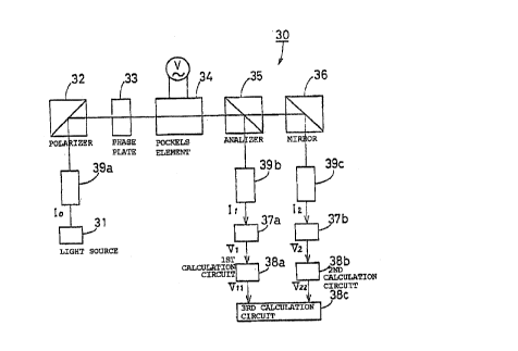
In Fig. 1 of the dr~wlngs, there ls schem~tically
111ustrated a preferred embodlment of an optlcal voltage-
electric fleld sensor 30 ~ceordlng to the present lnven-
tion. The optlcal voltage~electric field sensor 30 ln-
eludes a llght source 31 in the form o~ a llght-emltting
dlode (LED). a polarizer 32, a guarter-wavelenglh plate 33,
a Pockels element 34, an analyzer 35, a tot~l reflection
mirror 36, ~lrst and second light-recel~1ng elements 37a,
2 ~ ~4~78
37b, and ~irst, second and third calcuation circuits 38a,
38b and 38c. Thc- optlcal voltage~electric field sensor 30
~urther includes a rod lens 39a arranged belween the li~ht
sour_e 31 and polarlzer 32 nn~ a palr o~ rod lenses 39b,
39c which are arraneed respectlvely between the analyzer 35
and llg~t-receivlng element 37a snd between the tot~l
reflectlon mlrror 38 and llght-recei~ing elemen~ 37b. In
the optlcal Yoltage electric field seDsor 30, a llght beam
Io emanated from ~he ~lght source 31 is transmltted through
an optlcal ~iber to ~he rod lens 39a an~ received by the
polarizer 32 as parallel light bea~s from the rod lens 39a.
The polarizer 32 convert6 the lncident parallel li~ht beams
into a linearly polarlzed liFht beam, and the Pochels
element 34 recelves the llnearly polarized light beam ~rom
polarizer 32 throu6h the quarter-wavelerlgth piate 33 to
modulate the llnearly polarized lieht bea~ in accordance
wlth a ~oltage or electric fleld applled thereto. The
quarter-wavelength plate 33, Po~kels element 34, analyzer
35 and re~lectlon mirror 36 are arranged in series on th~
li~ht transmission path of the llnearly pol~rize~ llght
beam.
The quart~r-wavelength plate 33 ls made o~ rock cr~stal
and l~ arran~ed in such a manner that ~he ~rlncipal ~xls
dlrection of lndlcatrlx ls located at 45' relati~e to the
polarlzation plane of the llnearly polarized li~ht bea~ to
apply a phase dl~fere~ce o~ ~ to the llnearly polarlzed
llght ~eam. The Poc~els element 3l is made of a single
~ ~4~
crystal of Li~bO3 and is arraneed ln ~uch a manner tha~
a z-axls o~ the crystal ls placed ln parallel wlth the
llght axls and ~hat the principal axis directlon o~ lndlca-
trix of the quarter-wavelength plate 33 colncldes wlth
optical axes x' and y' defined by the fol~owlng ~ormula.
x' = ~ 2)1/2] (X - y)
y~ ~ [lj(2)1J2l ~X t y)
The Poc~els element 34 18 yrov~ded wlth electrods to be
applled wlth an AC voltaFe.
The analyzer 35 separates the modulated Incldent light
beam lnto a S-polarized li~ht beam ln a ~lbrative dlrection
perpendicular to the plane of the light beam and a P-
Folarlzed li~ht beam in a vibratiYe dlrectlon par~llel with
the plane of the lncldent llght beam. The S-po]~rized
li~ht beam i9 emansted in a directlon perpendlcular to the
lncident ~lght beam, ~hlle the P-polarlzed llFht bea~ is
e~anated in the ~ame direction as the incident light beam.
The S-polarlzed light beam transmltted from ~nalyzer 3~ is
conden~ed by the rod len~ 38b nnd received by the ~irst
light recelving element 37a, whlle ~he P-polarlzed lldlt
beam reilected by mlrror 36 is condensed by the rod lens
3~c and received by t~e second lig~-recelving element 37b.
The ~lrst l.ight-recelving elemçnt 37a convert~ the S-polar-
lzed lieht beam into a ~I.rst electric signal Yl lndlcatlve
o~ the ll~ht lntensitY rl t~ be calculated by the ~irst
calculatlon circu~t 38a, while the second l~ht-recel~lng
el~ent 37b converts the P-polarized lJght beam lnto a
second electric eignal V2 lndicatlve o~ the light intensl~y
4~8
I2 t~ be calculated by the second calculation circult 38b.
The first calculation circult 38~ caloulates an equa-
tion Vll - (Vl - DCl)/DCl based on the f~rst electric
slgnal Vl to produce an output signal Vll therefrom. whlle
the second calculatlon clrcuit 38b calculates sn equ~tlon
V2~ = (V2 - DC2)/DC2 to produce an output slgn~l V22 there-
from. In the equatlons. DCl is a dlrect current component
o~ the flrst electrlc slFnQl Vl, and DC2 is a direct cur-
rent component of the second electrlc signal v2 The thlrd
calculation clrcuit 38c calculates an equation V3 ~
l~[(a/V~ V22)l based on the output signals Yll~ V22
to produce an OUtpU~ slgnal V3 there~ro~. As6umlng that
the lntenslty of the lncldent llght beam from the llg~lt
source 31 ls Io and that each value of a, ~ is "1", the
respectlve intensities Il, l2 of the output liFht beams
recelved by the rlrst and second llght-receiving elements
3~8, 3~b are represented by the follo~lng equations (3),
(4), and the output slgnals Vll, V22 are repre~ented by the
fo}lowln~ equ~tions (5), (6).
Il 5 (1o/2) (1 - rz - k-~T) .. .. (3)
I2 = (Io/2) (1 ~ rz ~ k-~T) .... (4)
Vll - (Vl - ~Cl)~DCl = (-rz)/(l - k~T) ....
V22 ' (V2 - DC2)/DC2 = (rz)~ k ~T) .... (6l
Thus, the output si~nal. V3 Or the thlrd calculatlon clrcult
38c ls repre~ented by the followlng equations (7) ~nd (8).
V3 = l/~(~/V~ /V22)]
V3 = l/[(l~Vll) ~ (l/V22)l
- 1/[ (-1 ~ k~T)lrz - (1 I k-~T)~rz]
- 14 -
~P ~97~
~ -rz~2 .... ~8)
Accordln~ly, ~he output V3 expressed by the equ~tlon
(8) ls not depcndent on tbe temperature charaeteristic
property o~ double re~raction ln the quarter-wavelength
plate 33.
Assuming that ~he respect~ve values o~ a, ~ are not
~1~, they are prellmlnar11~ determined on a basls of the
~ollowlng equations (9) and (10~.
[ a /V~ T - 01 ] - [ B ~V22 ( ~ T ~ )
= [~/V~ T - TL-25)) - t~/V22(aT = T~ 2~)] .... (9
la/vl~ T - o)] - [B~V22(~T ~)~
= [a/V~ T = TL-25)~ - [~/Vz2(~T TL 25)~ ...( )
In case the respectlve intensities Il, I2 of the output
light beams are changed respecti~ely by l/A, l/B due to
unexpected lnfluence such as external disturbance, they are
represented by the iollo~ing equatlons (11). (12).
Il = (Io/2A) (1 - ~z - k ~T) ....(11?
- I~ = (Io/2B) (1 ~ rz + k-~T) ....tl2)
Thus, the output signals Vll, Y2~ of the ~lrst and second
c~lculatlon circults 38a, 38b are represented by the iol-
lowlne equation6 (13), tl4).
Vll = (Vl - DCI)/DCl ~ (-rz)/(l - k~T) ....(13)
V22 ' (V2 ~ ~2)/DC2 = (rz)/(l ~ T) ....(14)
As ~ result. the output slgnal V3 1s repre~ented by
l/~ tl~V~ 22) r~/
Ae~ordin~ly. the output V3 o~ the thlrd calculatlon clrcult
- 15 -
~ ~04Q7~
38c i~ not dependent on the temperature characterlstic
property of double refraction in the quarter-wavelength
plate 33.
In Fig6. 2, 3 and 4, there are lllustr~ted respective
chanee ratlos of the outputs Vll, V22, V3 in relatlon to
the temperature of the sensor. In a maximu~ operatlng
standsrd temperature range (-20'C to 80 C) of the 6ensor,
the outputs ~'11 and V22 represent opposlte temper~ture
characterlstics, and the output V3 is not influenced by a
change o~ the temperature.
Experlment:
A number o~ the optical voltage electric fleld sensors
according to the present in~el~tlon and conventional sensors
shown in Flgs. 5 aIId 6 ha~e been manufaetured to observe
fluctuatlon oi the output V3 in the case that the ~empera-
ture of the sensors wa6 changed in the maximum operating
standard temperature range (-20 C to 80 C~ ~nd that a
transmission ~mount of the llyht be~ms among the optic~l
parts was changed. The result of the obser~atlon was
obta~ned as descrlbed below.
1) In the three klnds of sensors. the output V3 was
proportl~na} to the voltage apPlled thereto.
2~ Tn regard to fluctustion of the output caused by the
temperature change, the outputs of the c~n~enti~nal sensors
o~ about 80~ were fluctuated, while nny fluctuation of the
output wa~ not ~ound in the sensors according to the
Present invention.
4Q~
3) In regard to ~luctuation of the output caused by
change oi the transmi~slon amount of the light beam, fluc-
tuation o~ the outputs was found in the conventional sen-
sors of about 50%, while an~ fluctuatlon Or the outpu~ ~as
not iound ln the sensors Accordlng to the present lnven-
tSon.
Although Sn the above preferred embodiment. the presentinventlon has been adapted to the optical volt~ge~electric
ileld sensor whereln the polarizer 32, phase plate 33,
Pockels element 34 and a~alyzer 35 are arranged in sequence
on the light transmisslon path of the llght beam, it ls
obvious to one oi ordlnary skill ln t~e ~rt that the
present lnventlon may be adapted to an optlcal voltage.
electric field ~ensor wherein the polarizer 32, Pockels
element 34, phase pl~te 33 and analyzer 35 are arranged ln
sequence on the llght transmlss~o~ p~th oi the light be~m.