Note: Descriptions are shown in the official language in which they were submitted.
-- -~-105107
FIELD OF THE INVENTION:
This invention relates to signal generators
and in particular to a current controlled oscillator for
use in a phase locked loop.
BACKGROUND TO THE INVENTION:
Phase locked loops utilize voltage controlled
oscillators to maintain phase and frequency stability,
wherein a control voltage resulting from a comparison
between an output signal and a reference signal is used
to control the phase and frequency of an oscillator.
However it is common that rather than a voltage
controlled oscillator, a current controlled oscillator
is used, with a voltage to current converter feeding it,
wherein the control voltage signal is applied to the
voltage to current converter.
The input voltage to the converter is
typically obtained from a charge pump and loop filter
combination as described by F. Gardner in "Charge-Pump
Phase Lock Loops", IEEE Transactions on Communications
28; 1849-58, November 1980. In a single V/I converter
the single charge pump voltage is compared to a supply
voltage or some process dependent voltage such as VT in
a MOS. In the differential case, an output of a phase-
frequency detector is a series of "up" and "down" pulses
which are used to control a differential charge pump.
These up and down pulses are proportional to the phase
difference of the inputs to the detector. When
connected to a differential charge pump, the result is a
voltage difference which is also proportional to the
phase difference of the inputs. This voltage difference
is applied to a differential voltage to current
converter, the output of which is applied to a current
controlled oscillator.
A "pseudo-differential" scheme may be used
where the input voltage is compared to a locally
210 .~107
generated voltage reference. The differential and
pseudo-differential schemes allow the current to be
steered such that the minimum current is zero and the
maximum current is equal to ~2 (the frequency/current
gain factor within the current controlled oscillator)
times a well-controlled constant bias current.
To ensure loop stability across a wide range,
to minimize jitter, and to control frequency acquisition
times, it is often desirable to have the gain constant
of the phase locked loop programmable. This is commonly
accomplished by altering device sizes within the current
controlled oscillator, by switching in delay elements
within the current controlled oscillator, or by changing
current mirror ratios within the voltage to current
converter. The gain of the phase locked loop may be
controlled by altering the bias current, the voltage to
current gain constant and the current controlled
oscillator gain constant. However this also affects the
frequency of the oscillator. The maximum operating
frequency is set by the gain constants and the minimum
frequency is equal to zero.
SUMMARY OF THE INVENTION:
The present invention provides independent
control of both the frequency of the oscillator and the
gain of the phase locked loop. The gain constant and
frequency in the present invention are each separately
digitally programmable.
In accordance with an embodiment of the
present invention, a voltage to current converter is
comprised of a first current steering mirror for
receiving an input voltage signal and converting the
voltage signal to an output current, and being comprised
of first binary weighted current mirror transistors, a
second current mirror for generating a selectable output
current, the second current mirror being comprised of
'~ - 2 ~031 0 7
second binary weighted current mirror transistors,
apparatus for adding the output currents, and apparatus
for providing the added output currents to a control
input of a current controlled oscillator.
S In accordance with another embodiment of
the invention, a converter is comprised of a voltage to
current converter, apparatus for controlling the gain of
the voltage to current converter, a separate current
generator, apparatus for controlling current emitted
from the current generator, apparatus for adding output
current signals of the voltage to current converter and
the current generator and for providing a sum signal to
a current controlled oscillator.
In accordance with another embodiment of
the invention, a phase locked loop is comprised of a
phase-frequency detector, apparatus for providing a
reference signal and a controlled signal to the
detector, apparatus for providing a voltage signal
resulting from the detector detecting a difference
between the phases of the reference and controlled
signals, a first current steering mirror for receiving
the voltage signal and converting the voltage signal to
an output current, and being comprised of first binary
weighted current mirror transistors, a second current
mirror for generating a selectable output current, the
second current mirror being comprised of second binary
weighted current mirror transistors, apparatus for
adding the output currents, apparatus for providing the
added output currents to a control input of a current
controlled oscillator, and apparatus for providing an
output signal of the oscillator as the controlled signal
to the detector.
BRIEF INTRODUCTION TO THE DRAWINGS:
A better understanding of the invention will
be obtained by reference to the detailed description
~4~ 2103l07
,, .
below, in conjunction with the following drawings, in
which:
Figure 1 is a block diagram of a phase locked
loop in accordance with the prior art,
Figure 2 is a more detailed block diagram of
the analog portion of a phase locked loop in accordance
with the prior art,
Figure 3a is a block diagram of the voltage to
current converter and current controlled oscillator in
accordance with the prior art,
Figure 3b is a more detailed illustration of a
typical current converter with a current controlled
oscillator,
Figure 4a is a block diagram of the voltage to
current converter and current controlled oscillator in
accordance with the present invention,
Figure 4b is a diagram of the present
invention, and
Figure 5 is a graph of frequency/voltage
transfer curves.
DETAILED DESCRIPTION OF THE INVENTION:
A typical phase locked loop is shown in Figure
1. This structure is comprised of an analog portion 1
having a reference input (for receiving a clock signal)
and a frequency input (for receiving a comparison
signal), and a controlled voltage output signal Vcout.
The phase locked loop includes a digital portion 2 which
includes a divide by N counter 5, which presents a
signal to the frequency input of the analog portion 1 in
phase with the output signal. Clock signal Ckin is
provided to an optional divide by M counter 7, the
output of which is applied to the reference input of the
analog portion. Control logic 9 controls the operation
of the analog portion 1.
210S107
Figure 2 is a more detailed block diagram of
the analog portion 1. A phase-frequency detector 11
receives the Ckin reference and Ckfeed frequency inputs,
and outputs up and down signals to a charge pump 13.
s The output of the charge pump is a control voltage for
application to a voltage controlled oscillator, the
output voltage of which is proportional to the phase
difference between the reference signal Ckin and the
feedback signal Ckfeed at the frequency input.
Rather than utilizing a voltage controlled
oscillator, current control oscillators are often used
as shown in Figure 2. A voltage to current converter 15
receives the output signal voltage of the charge pump 13
and provides a control signal current to current
controlled oscillator 17. The output of oscillator 17
is applied to an output buffer 19, if the buffer is not
already part of the oscillator 17, to provide a
controlled output signal Vcout 21.
A loop filter 23 is connected at the output of
charge pump 13, and a voltage reference circuit is
connected to the charge pump 13 and converter 15.
Operation of the above-described circuit is
well known and is described in "Charge-Pump Phase Lock
Loops" by F. Gardner, IEEE Transactions on
Communications, Vol. Com-28, No 11, November 1980.
Turning to Figure 3a, a prior art voltage to
current converter 15 is illustrated, the current control
signal output being connected to the input of a current
controlled oscillator 17. Input signals to converter 15
are the control voltage from the charge pump 13 and a
bias current IbiaS~ from a reference voltage current.
Figure 3b is a more detailed illustration of a typical
current converter with a current controlled oscillator.
~ - - 2105107
The gain of the phase locked loop is
controlled by a number of factors, including
contributing factors ~1 and ~2 in which
~ V, the current/voltage gain factor
S within the voltage to current converter 15, and
~2 = ~f/ ~I, the frequency/current gain factor
within the current controlled oscillator.
In accordance with this prior art
configuration, the frequency of the output signal of
current controlled oscillator f=Vin-~1- ~2Ibias ~ In order
to vary the gain of the loop, the bias current is
required to be varied, or the V/I gain constant, and the
current controlled oscillator gain constant. However
these variations affected the frequency range of the
oscillator.
The present invention provides apparatus for
digitally programming the gain constants and the
frequency control. A block diagram of the present
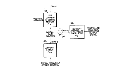
invention is shown in Figure 4a.
In the present invention a current steering
mirror 30 receives the control voltage and bias current
IbiaSl as inputs. A programmable digital gain control
signal is applied to current steering mirror 30. A
current mirror 32 receives a programmable digital
frequency offset control signal, as well as a current
bias Ibias2
The outputs of current mirrors 30 and 32 are
summed in adder 34, and the sum is applied to current
controlled oscillator 36, the output of which is the
controlled frequency output signal.
Realization of the circuit of Figure 4a
according to one embodiment is shown in Figure 4b. The
input control voltage e.g. from a charge pump in a phase
locked loop is applied to current steering mirror 30
which receives bias current from current source 38.
~7~ ~ 1 ~ 5 ~ ~ 7 ''J
Current mirror 32 receives bias current Ibias2 from
current source 40.
Current mirror 32 controls the gates of field
effect transistors 41 and 42. The sources of
s transistors 41, 42 are connected to ground via
programmable switches 45. Current steering mirror 30
controls the gates of field effect transistors 46, 48
and 50. The sources and drains of transistors 46 and 48
are connected via programmable switches 52 to ground.
The drains of transistors 40, 42, 46, 48 and
50 are connected together at a mutual sum point 51.
This mutual sum point is connected to the input of
current mirror 54, the output of which is a current
control voltage for application to the input of a
current controlled oscillator, e.g. 36 as shown in
Figure 4A.
Programmable switches 45 control the frequency
offset of the current controlled oscillator, and
programmable switches 52 provide a digital gain control
for the current controlled oscillator.
Now the basic control equation for the above
circuit is as follows:
f = a2(vin ~ aIbiasl+ ~ bIbias2)
a2 = fixed
a1a = programmable
a1b = programmable
and wherein /1designates programmability of the gain
factor.
It may be seen that the gain constants in this
structure are digitally programmable by using binary-
weighted current mirror transistors within the voltage
to current converter block of the phase locked loop.
Transistor 50 is also preferably always included
regardless of the programming bits, in order to inject a
.~ '
-- 2 1 0 ~ 1 07
minimum current into the sum point, and thus establish
an initialization frequency control current.
With two bits of control for each ~f ~la and
~lbl the frequency/voltage transfer curves are as shown
in Figure 5. It may be seen that a wide and digitally
controllable frequency may be obtained without requiring
variation of the device sizes, without switching in
delay elements within the oscillator, without changing
current mirror ratios within the oscillator, and without
altering the master bias current. The frequency range
may be adjusted independently of the gain, allowing for
high frequency operation with moderate gain factors. A
more easily and more definitely controllable phase
locked loop results.
A person understanding this invention may now
conceive of alternative structures and embodiments or
variations of the above. All of those which fall within
the scope of the claims appended hereto are considered
to be part of the present invention.