Note: Descriptions are shown in the official language in which they were submitted.
1~~.~~~
TMAGE PROCESSING APPARA'fLTS
TEC~racAi. FaErn
The present invention is related to an image processing
apparatus, and more particularly to a game computer which
displays image data using an interlaced display system.
NACKG~tOUND OF T~iE INVENTION
Tn conventional image processing apparatus, two kinds of
display mode, namely, an interlaced and non-interlaced mode,
are used to display image data. Generally, the interlaced
display mode is used for TVs of an NTSC (National Television
System Committee) type, and the non-interlaced display mode
is used for computer image processors.
According to the interlaced display mode, 525 scanning
lines are divided into odd numbered fields and even numbered
fields, and the two kinds of fields are scanned alternately
so that the image is displayed clearly due to an
"after-image" phenomenon. For that reason, the interlaced
display mode is suited for TV images which are generally
camera images displayed for relatively long intervals.
According to the non-interlaced display mode for RGB
data, the 263 scanning lines of the even numbered fields or
the 262 scanning lines of the odd numbered fields are
selectively used for image display. Image data are supplied
to a VRAM (Video TtAM) during a horizontal retrace period, and
the image data are transmitted through a video encoder to a
display device in accordance with a predetermined
synchronizing signal.
The computer image processor handles both still and
moving pictures. In such a processor, if a moving picture is
redisplayed at short intervals using the interlaced mode, the
displayed image appears to have notched edges. Furthermore,
the interlaced. mode requires approximately twice as much
display information as the non-interlaced mode to display the
same image. Nevertheless, the image data must be transmitted
and processed with exact timing to display an image in the
interlaced display mode.
Process periods for different image data depend on the
type of data arid the amount of data to be displayed.
Consequently, the timing of the output of image data is
necessarily different for each image to be displayed.
Therefore, the transmission periods of the image data must tae
precisely controlled when a variety of images are
superimposed, and, the CPU must control each peripheral
20 device with precise timing. However, it is difficult to
control peripheral devices with precise timing using a
conventional computer because the image data are transmitted
to the display device in synchronization with the vertical
synchronizing signals.
SUMNdARY OF THE INVENTION
It is an object of the present invention to provide a
high performance computer in which peripheral devices axe
controlled by a CPU using precision timing.
20 According to the invention, in an image processing
apparatus, pixel clocks, hereinafter referred to as °°dot
clocks'°, and horizontal synchronizing signals are
respectively counted. The apparatus determines whether odd
or even fields of an image are being displayed, whether it is
25 a display period or a retrace period, and a value (number) of
the raster bring displayed, using the counted values. The
accumulated information is stored in registers, and a CPU
controls peripheral devices in a precisely timed manner
governed by the data stored in the registers.
That is, an ODD/EVEN signal showing whether odd fields
or even fields of an image are being displayed is supplied to
each peripheral device operating to transmit data. In
response to the ODD/EVEN signal, a horizontal and vertical
synchronizing composite pulse for either the odd or the even
field scanning operation is generated. The composite pulse
is superimposed on a Y signal to obtain a video signal for
performing an interlaced display.
2 ~~. ~ ~ :~. ~ ~.
- 3 -
Tn the interlaced display mode, picture elements are
shifted on a screen by 1/2 dot for each alternate scanning
line so that output distortion and roughness at the edges of
the image are reduced. The CPU monitors the condition of the
displayed image so that data transmission and processing, and
use of a data bus may be controlled with precise timing.
Consequently, each unit in the apparatus may be operated
effectively, and as a result the apparatus may process a
variety of types of image data at high speed.
1Q
s~IEF D~sc~P~raorr of ~ D~waaaos
Fig. 1 is a block diagram illustrating a computer system
of a preferred embodiment in accordance with the invention;
Fig. 2 is a block diagram illustrating a video encoder
25 unit used in the preferred embodiment shown in Fig. 1:
Fig. 3 is a diagram showing displayed pixel data,
hereinafter referred to as dot data in a non-interlaced mode
of operation of the preferred embodiment;
Fig. 4 is a diagram showing displayed dot data in an
20 interlaced mode, of operation of the preferred embodimentv
Fig. 5 is a diagram showing displayed dot data in the
interlaced + 1/2 dot shift mode of operation of the preferred
embodiment:
Fig. 6 is a diagram showing an arrangement of an address
25 register used in the preferred embodiment:
Fig. 7 is a diagram showing an arrangement of a status
register used in the preferred embodiments
Fig. 8 is a diagram showing an arrangement of a control
register used in the preferred embodiment; and
3o Fig. 9 is a table showing the contents of the control
register shown in Fig. 8.
DETAILED DESCRIP'.rIOT1 OF THE II~IVENTIOld
Hereinafter, a computer apparatus in accordance with a
35 preferred embodiment according to the present invention will
be explained in conjunction with the appended drawings.
2~~~.~.~~
_4_
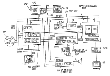
Fig. 1 shows an information processing system of the
preferred embodiment. The information processing system
includes a recording medium 100 such as a CD-ROM for
game-software, a 32-bit CPU 102, a control unit 104 used
principally for controlling transmission of image and sound
data and acting as an interface between most devices, an
image data extension unit 106, a sound data output unit 110,
a video encoder unit 112, a VDP unit 114 and a TV display
monitor 116.
CPU 102, control unit 104, image data extension unit 106
and VDP unit 114 are provided with their own memories K-RAM
118, X-RAM 120, R-RAM 122 and V-RAM 124, respectively.
CPU 102 directly controls a DRAM 126 via a memory bus
and a memory support function, and communicates through an
I/O port with peripheral devices (not shown), that is, i~t
performs an I/O control function. CPU 102 includes a timer,
a parallel I/O port and an interrupt control system.
VDP unit 114 reads display data which have been written
into the VRAM by CPU 102. The display data are transmitted
to the video encoder unit 112 which processes the data for
display on the TV display monitor 116.
Control unit 104 includes a SCSI controller to which
image data and sound data are supplied through a SCSI
interface from CD-ROM 100. Data supplied to the SCSI
controller is buffered in the K-RAM 118. Control unit 104
also includes a DRAM controller for reading data which have
been buffered in the K-RAM 118 at a predetermined timing. In
control unit 104, priority judgement is carried out
dot-by-dot for image data of a natural background, and its
output signal is supplied to video encoder unit 112.
Control unit 104 transmits moving image data (full
color pallet), which has been reduced in size, to an image
data extension unit 106 where the compressed data are
decompressed. .The decompressed data are transmitted from
image data extension unit 106 to video encoder unit 112.
~:~~la~.~~_
_ 5 _
Video encoder unit 112 superimposes VDF image data, the
natural background image data and moving image data
transmitted from VDP unit 114, control unit 104 and image
data extension unit 108, respectively, Video encoder unit
112 performs color pallet reproduction, special effect
processing, D/A conversion and the like. O'utpu't data of
video encoder unit 112 are converted to an ;~TTSC signal by an
NTSC converter 125.
ADPCM sound data recorded in CD-ROM 100 are buffered in
the K-RAM 118 and then transmitted to sound data output unit
110 by control unit 104. The sound data are reproduced by
sound data output unit 110.
In this preferred embodiment, the original output signal
of a 43MHz oscillator is used as a system clock OSC of
43MHz. The system clock OSC is divided at a frequency
dividing ratio of 2 by a clock control circuit in the image
data extension unit to generate a system clock SCK of 2lMHz.
When a color chrominance subcarrier of 12 times the
frequency is supplied to a synchronizing signal generating
circuit 128 of the video encoder unit 112 (see FIG. 2), dot
clock signals of the frequency dividing ratios of 8 and 6 are
generated.
When the system clock OSC of 43MHz is supplied to the
synchronizing signal generating circuit 128, the system clock
is divided at the frequency dividing ratio of 8 to generate a
dot clock DCKKR whereby a screen mode having 256 dots for
each raster is accomodated. Further, the system clock OSC of
43 MHz is divided at the frequency dividing ratio of 6 to
generate a dot clock DCK70 whereby a screen mode having 320
dots for each raster is accomodated.
The synchronizing signal generating circuit 128 also
supplies horizontal synchronizing signal -HSYNCA, -HSYNCB and
-HSYNCC, and a vertical synchronizing signal -VSYNC. The
synchronizing signal generating circuit 128 is supplied with
external horizontal and vertical synchronizing signals
whereby an image may be displayed in synchronization with an
external input.
2~.~~:~~~.
In the video encoder unit 112, the dot clock DCK and
horizontal synchronizing signal -HSYNC~1 are counted to create
internal signals indicating whether an image is displayed in
the odd fields or even fields, and whether the image bea.ng
displayed is in a display period or a retrace period of the
horizontal and vertical periods. These data are stored in a
status register of the video encoder unit 1.12 together with a
raster count (raster number) of the horizontal display period
so that the CFU can monitor the current condition of the
displayed image.
In this preferred embodiment, the VDP unit handles two
sprite images (SP) and a background image (BG), the control
unit 104 handles four background images BMGO, BMG1, BMG2 and
BMG3, and the image data extension unit 10& handles an IDCT
(Huffman encoded data) J RL (run-length) image, respectively.
Sound data output unit 110 handles 6 channel PSG
waveform data and 2 channel ADPCM waveform data.
CPU 102 is enabled to write data which define the BG and
SP data of the 'VDP, write the PSG data, and write data into a
color pallet RAM. The CPU controls the control unit 104 to
convert an image and transmit DMA data. The CPU also
controls an image synthesizing process such as a chromakey
process and a cellophane process, and an image superimposing
process based on a predetermined priority.
Fig. 2 shows the video encoder unit 112. The video
encoder unit is composed of an IC including the synchronizing
signal generating circuit 128, the color pallet RAM 130, a
priority arithmetic circuit 132, a cellophane arithmetic
circuit 134 (for synthesizing upper and lower pictures), a
D/A converter for an image signal (not illustrated), an 8/16
bit data bus (M-bus) interface 146, a VDP interface 140, a
control unit interface 142 and an image data extension unit
interface 144.
Figs. 3 to 5 show images displayed in a non-interlaced
mode, common interlaced mode, and in the interlaced mode with
a 1/2 dot shift function, which will be explained
below.
The video encoder unit selects one display mode from the
interlaced and non-interlaced modes. In the interlaced mode,
scanning lines are fixed in number at 263 or 262, an O/E bit
at an address 03E of the status register is set at °'1" during
an odd field display period in a first 1/60 second period so
that an image is displayed as in the non-interlaced mode.
During the next 1/60 second period, that is, in an even field
display period, the 03E bit becomes "0°' to display an image
located 1/2 line above the precious image. As a result, the
distance between the first (odd) and second (even) fields is
very narrow, and the image is displayed smoothly. These
processes are repeated alternately.
If the same pictures are displayed alternately on the
odd and even fields, the image appears as if it is vibrating
up and down at a short intervals.
In the interlaced mode, the image is displayed
field-by-field at the exact same positions on the display
screen whereby a desired image is displayed clearly.
Furthermore, it is possible to display a higher quality image
by using a 1/2 dot shift function for the display. According
to the 1/2 dot shift function, picture elements pixels are
shifted 1/2 dot in a horizontal direction at one line
intervals. In this function, a mask is used for smoothing
notched edge lines of the image, and as a result, the
displayed image is composed of 255.5 dots per scanning line.
In the D/A converter of the video encoder 112, a 'YUV
signal of 8 bits is converted into an analog signal. If a W
signal has only 4 bit data, such as color pallet data, the 4
bat data padded on the left with "0000" to make up 8 bit
data. The X data are converted into an analog signal in a
linear fashion, for example, °'00h" data is converted into a
black color signal and "FFh" data is converted into a white
color signal. The U and V data are also converted into
analog signals in a linear fashion; however, data over "80h°°
is expressed as a positive analog signal and data under "80h"
is expressed as a negative analog signal, because the U and V
~3.~~~.~~.
_$_
data are color difference data expressed as analog signals
having positive and negative polarities.
A color to be expressed has a color depth defined by a
value of a difference between the U and i7 data and "80h'°, so
that the colors represented by '°OOh°° and
°°FFh°' are the
deepest, and no color is expressed when eaclh of the U and v
is '°80h". Color hue is represented by a ratio between the
values of a difference between the respective U and t1 signals
and '°80h=', and the polarities of each difference.
In the D/A conversion process, the Y signal may be
modulated with a synchronizing signal, and 'the U and V
signals may be modulated with chrominance subcarrier. T~
chrominance subcarrier modulation is selected, color burst is
superimposed on the U signal at a predetermined timing and
amplitude. The D/A converter is of a current adding type,
that is, a voltage conversion is carried out in accordance
with an input impedance of external circuits.
To generate an RGB signal, an analog arithmetic function
is used by a predetermined external circuit to time the Y
signal without a synchronizing signal and to time the
unmodulated Uv signal. The synchronized Y signal with and
the modulated UV signal are mixed by an external circuit to
generate a composite video signal for the CRT display monitor
116.
?.5 Figs. 6 to 8 show arrangements of an address register, a
status register and a control register in the video encoder
unit 112. The status register and control register are
accessed indirectly using the address register.
The address register (AR) specifies internal registers
R00 to R15 in the video encoder unit 112. The status
register stares information relating to a current status of
the displaxed image.
In the status register:
(a) An °'AR'° in the 0th to. 4th bits indicates the
current address of the address register.
2:~~V:~~~. ,
(b) A "RASTERCOUNT°' in the 5th to lard bits indicates a
raster number of the current display in the display period of
22 to 261. The raster number set at the °'RASTERCOUNT°°
does
not correspond to a scanning line number defined by the NTSC
signal. The raster number becomes '°IFFh" when an external
synchronizing signal is distorted.
(c) An "0/E" at the 14th bit indicates whether an image
is displayed in the odd fields (1) or the even fields (0) in
the interlaced mode.
(d) A °'DISP'° at the 15th bit indicates whether the
video encoder 112 is working in a display period or a,retrace
period (H blank, V blank). A '°0" and "1°' are set at the 15th
bit during the display period and the retrace period,
respectively.
In the control register (CR > R00), the 8th to 14th bits
and the others are available during the following horizontal
and vertical periods, respectively:
(a) A '°DCC°' at the 0th and first bits indicates whether
the current mode is the interlaced or the non-interlaced
mode, as shown in Fig. 9.
(b) An "EX" at the second bit indicates whether an
external synchronization is executed. When '°1°' is set at the
second bit, unsynchronized operation is performed until an
external synchronizing signal of proper frequency is
detected, and then the operation is synchronized. On the
other hand, when the second bit is set at "0", the external
synchronizing operation is generally reset. However, in some
cases the external synchronizing operation may be reset if
the external synchronizing signal is very distorted.
(c) A "DCT7" at the third bit indicates that an image
is displayed with 320 dots in the horizontal direction. When
the third bit is set to "1°', the 320 dot horizontal display
is specified. In this mode, the dot clock of the VDP unit
operates at only a 7NdHz frequency, and the cellophane
function is disabled. ..,
~2~:D5 ~ ~~
- 10 -
(d) A "Blanking bits'° in the 8th to lath bits indicate
which of the pictures BG, SP, BMO, BM1, BM2, BM3 and ~2A7CN
respectively are displayed. The instruction is available
after each horizontal period. If all the °'blanking" bits are
set at '°0", that is, are reset, a black color is supplied as
a YUV output (Y=OOh, U=80h and V=80h).
The operation of the address and status register will
now be explained.
Step 1 : -CET (chip enable) and A1 terminals are set at
°'L°° whereby the address register (AR) is accessed.
Then, a
register number of a register to be accessed next is written
in the address xegister.
Step 2 : The A1 terminal is changed to °°H" while the
-CBT terminal is left at "L'°, whereby the register written in
the address register is selected. Then, predetermined data
are written into or read from the selected register.
During these steps, the contents of the address register
is maintained at the initial value until the address register
is rewritten. Therefore, the first step may be omitted when
the same register is again accessed.
When the address register is read, the register is
changed to the status register. The status register stores
current information such as whether a display period or
retrace period is currently being executed, whether the
displayed image is being displayed in odd fields or even
fields, and the number of rasters that have been displayed
during the display period.