Note: Descriptions are shown in the official language in which they were submitted.
-~ ~1 a~6Ll
BACKGRCll3ND OF THE INVENT10N :
1. Field of the Invention
The present patent relates to methods to continuous-
ly deposit large area thin films of semiconductors such as
CuInSe2, CdTe and CdS and to continuously fabricate thin
film photovoltaic cells.
:::
~ 2. Description ~f the Prior Art
~ .
The semiconductors CuInSe2, CdTe, CdS and ZnO are
ideal materials for the fabrication of photovoltaic cells.
For the photovoltaic cells, thin film form semiconductors
must be deposited on large area substrates. Large area thin
film deposition using conventional vacuum methods, however,
is costly. For large area applications, it is required that
the films be prepared using lower cost methods than the
vacuum methods currently emplsyed. Low cost thin film
,, ~
deposition methods currently used include screen printing,
spray pyrolysis and electrodeposition. Of the three meth-
ods, electrodeposition is the most appropriate, because
electrodeposition consumes less energy and produces better
~:
films.
;~ ` 2 ;
: '~
210 ~4fi4
. .
In a pending patent application No. 2,063,679-4
"Methods for the fabrication of CuInSe2 thin films and
solar cells" by I. Shih and C.X. Qiu (filed on November
11, 1991), methods for the electrodeposition of semiconduc-
tor thin films including CuInSe2 thin films have been
disclosed. In the methods described in the aforementioned
patent application, a substrate and an anode are immersed
in an electrolyte. A voltage is applied between the sub~
strate and the anode to deposit a semiconductor thin film
on the substrate. The substrate is removed from the elec-
trolyte and a new substrate is used for the sub~equent
deposition. Although the methods described allow ons to
deposit semiconductor thin films, they are not optimum for
large area thin film deposition and cell fabrication. It is
thus clear that there is a need to provide an improved
electrodeposition method which can produce semiconductor
thin films in a continuous manner.
For electronic device application, film composition-
al depth profile and average composition must be
controlled . For instance, in photovoltaic cells, the
compositional depth profile of the absorber material (such
as CuInSe2 and CdTe) must be maintained so that the first
layar (bottom layer which is adjacent a conducting sub-
s,J ~:
;1- strate) of semiconductor deposited is of high conductivity.
!
:i
2~ aa~4
The bottom layer of the deposited semiconductor must be
highly conductive to make low resistance ohmic contact with
the conducting substrate. The top layer is of relatively
low conductivity, so that a good quality heterojunction can
form when a window material such as CdS is deposited on the
surface. The electrical conductivity of a compound semicon-
ductor i6 often determined by the elemental composition.
For instance, high conductivity p-type CuInSe2 can be
obtained when the In/Cu in the films is slightly greater
than or less than 1. On the other hand, low conductivity
p-type or nearly intrinsic CuInSe2 can be obtained when
In/Cu is relatively greater than 1.
In the prior art electrodeposition methods for
compound semiconductors, the required compositional depth
profile for good quality heterojunctions was obtained by
controlling the deposition potential (or voltage) during
the film deposition. The variation of the potential or
voltage during the deposition process limited deposition to
stationary substrates. This is because when the substrate
is fed into the electrolyte continuously at a given speed,
the variation of deposition potential with time will result
in a non uniform semiconductor thin film over the film
area.
2hOa~61
During the electrodeposition, the ion concentration
in the electrolyte decreases with time. If the same elec-
trolyte is used for continuous deposition ~or compound
semiconductor thin films, the average composition of sam-
ples deposited at different times will vary. Therefore, the
ion concentration must be kept constant during the entire
deposition process i~ film composition is to be maintained. `~
From the above comment, it is clear that there is a
need to provide improved deposition methods for compound
semiconductor thin film and photovoltaic cell fabrication.
;~
'~ -~ ,.
, ~ ' ',` "
: ~ ...
~: .
,~ 1 ' ' ' '' ' '.
,~ .
~:
~ 5
~05~6~
OBJECTS AND STATEMENT OF THE PRESENT
INVEI ITION
One object of this invention is to provide an im-
proved electrodeposition method for the continuous deposi-
tion of thin films of semiconductors such as CulnSe2, CdTe
and CdS.
Another object of this invention is to present a
method to control the compositional depth profile of the
deposited compound semiconductor films.
Yet another object of this invention is to provide a
method to prepare compound semiconductor thin films with a
constant average composition.
, - ~; ~ ;,
'~'`'`':
-
:
~: 6
: ~; ~
'','.
~`~` 2 ~ 6 ~
BRIEF DESCRIPTION OF THE DRAWINGS -:
~.:
Fig. 1 is a schematic diagram showing the electrodeposition
apparatus for the continuous deposition of CuInSe2, CdTe,
CdS, ZnSe and ZnO.
Fig. 2 is a schematic top view of the electrodeposition
apparatus for the continuous deposition of semiconductor
thin films.
Fig. 3 is a diagram showing an arranqement of the anode
,:
and the substrate to obtain a graded compositional depth
profile.
Fig. 4 is a schematic diagram of the deposition system
with apparatus to add sources of ions to the electrolyte
and to circulate the electrolyte during the semiconductor
thin film deposition. - -
Fig. 5 is a diagram showing the apparatus used to rinse
, .;
the substrate after the semiconductor thin film deposition.
Fig. 6 is a schematic diagram showing a unit for the
continuous heat treatment of semiconductor thin films.
~;
; -
~5~6ll
Fig. 7 is a schematic top view of the heat kreatment
unit showing the distribution of the gas inlets.
Fig. 8 is a schematic diagram showing the dip coating
apparatus for the continuous deposition of CdSe, ZnS, ZnO
, and CdS.
I Fig. 9 is a schematic diagram of the semiconductor dip
coating system with apparatus to add sources of ions to the
electrolyte and to circulate the electrolyte during the
semiconductor thin film deposition.
Fig. 10 is a schematic diagram of a system for the con-
tinuous deposition and heat treatment of the first semicon-
ductor and the deposition of the second semiconductor.
Fig. 11 is a schematic diagram of a system for the con~
tinuous deposition of the ohmic contact material, the
continuous deposition and heat treatment of the first
semiconductor, the deposition of the second semiconductor,
.:
¦ the deposition of low resistivity window semiconductor and ~
.
~ the deposition of contact grids. ~
,~
6 il
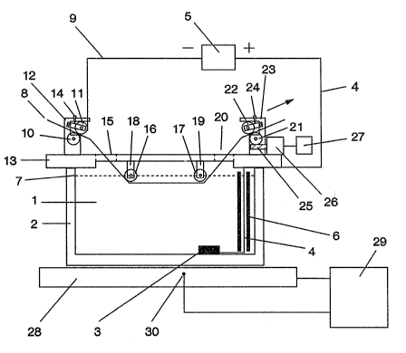
DESCRIPTION OF TIIE PREFERRED E~MBODINIENTS
The preferred system used in this invention for the
deposition of semiconductor thin films is illustrated in
Fig. 1. An electrolyte ~1) in a glass container (2) is used
for the deposition. The electrolyte consists of ions or
complexes of Cu, In and Se for CuInSe2 deposition, Cd and
Te for CdTe deposition, Cd and S for the CdS deposition, Zn
and Se for the ZnSe deposition, and Zn and S for ZnS depo-
sition. A small amount of acid such as HN03, HCl, H2S04 or
another ion source such as A12C13 is added to the electro-
lyte to adjust the pH value and to increase the conductivi-
ty of the solution. In plate or rod form, a conducting
anode (3), such as Pt or C, is placed in the bottom of the
deposition chamber. The anode is connected electrically
through a Pt wire (4) to a dc power source (5). A part of
the Pt wire (4) is inserted through an electrically insu-
lating glass tube ~6~. The top portion of the glass tube
" ~ ~
extends above the level (7) of the electrolyte. This glass
tube arrangement is important to obtain a well defined ~ --
electric line distribution between the anode (3) and the
substrate (cathode) (8).
, ~
g
1~ ~ ` '; ':
6~ ~
The other terminal of the power source (5) is con-
nected to the ribbon through another wire (9)~ The sub-
strate is a flexible ribbon of either Mo, Mo-coated brass,
Ni-coated brass or some other metals. The thickness of the
ribbon substrate is about 100 micrometers (~m). Thus the
ribbon is flexible enough to pass through the deposition
system. The ribbon substrate is Eed between two cylindrical
rollers (10, 11), which are attached to a support (12)
mounted on a top plate (13). One of the rollers (11) is
spring loaded (14) so that the ribbon substrate is pressed
between the two rollers. The two rollers are composed of
metallic material such as Ni-coated copper or brass to
achieve low resistance electrical contact. The ribbon is
inserted through an opening (15) in the top plate. When the
system is activated, the substrate will glide through the
electrolyte below and in contact with two glass rollers
(16, 17). The rollers are mounted on the bottom of the top
plate with two supports (18, 19). The supports are made of
electrically insulating and acid resistant material such as
~ i:
glass or Teflon.
The ribbon substrate is then fed through a second
~ ~ opening (20) in the top plate and finally inserted between
`~ two other cylindrical rollers (21, 22), which are fixed to ;
a support (23~ mounted on the top plate. One of the rollers
2la~
(22) is spring loaded (24) so that the ribbon substrate is
pressed between the two rollers. The other roller (21) is
connected through a worm gear (25) to a driving motor (26)
powered by an energy source (27). The rotation of the motor
is such that the roller (21) turns clockwise. The surfaces
of the two cylindrical rollers (21, 22) are either corru-
gated or coated with layers of plastic or rubber to in-
crease the friction, which is required to feed the ribbon
substrate through the unit at a constant speed. The depo-
sition chamber (2) is placed on top of an electric heater
(28~. The heater is powered by a second energy source (29)
with a temperature controller. The temperature of the
heater is monitored by a thermocouple (30), which is con-
nected to the temperature controller to regulate the output
power. The two electrically insulating rollers (16, 17) are
arranged so that the rollers are partly or completely
immersed in the electrolyte (1).
To initiate the film deposition, the electric power
to the heater (28) is turned on. The electrolyte is heated
to about 95C. The dc power source (5) connected to the
ribbon substrate ~8) and the anode (3), is activated. The
voltage is adjusted to a desired value. The power to the
driving motor (26) is then switched on so that the roller
(21) rotates at a constant speed, clockwise. The ribbon
1'' ~ 11
6 a~ :
substrate (8) is now fed from left to right through the
electrolyte at this constant speed. The compound semicon~
ductor thin film is deposited continuously on the sub-
strate.
Referring now to Fig. 2 for the top view of the
deposition chamber and for the preferred arrangement o~ the
anode (3) with respect to the ribbon substrate (83. During
the deposition, the ribbon (8), driven by the roller (21),
connected to the motor (26), travels from the left to the
right side of the chamber at a constant speed of v. The
elemental composition of an electrodeposited compound
semiconductor thin film is determined by the potential of
the cathode with respect to the electrolyte adjacent to it.
To obtain uniform semiconductor thin films (over the sur-
face), the anode (3) is placed perpendicular to the direc-
;~ .
tion of motion (31) of the ribbon. With the anode so ar-
ranged, the ribbon substrate will have the same potential
across its width ie. perpendicular to the traveling direc
tion of the ribbon, at a given position along its length.
The average chemical composition of the deposited compound ~;
semiconductor over the entire film will be constant. ;
The length, L (32), of the ribbon substrate (8) ~`~
immersed in the electrolyte (1), is slightly greater than
the separation between the two rollers (16, 17). The two
12 ~
:';
2 ~ 0 .~
rollers are partly or completely submerged in the electro-
lyte. When L is fixed, the feed speed of the ribbon sub-
strate, v, is governed by the deposition rate, d
(~m/minute), and the total thin film thickness, t (~m),
required. For instance, for a length L=10 cm and a deposi-
tion rate of 0.1 ~m/minute, the feed speed required to
deposit a thin film having a thickness t = 1 ~m is v = 1
cm/minute. With this feed spe~d and this length, the total
time that any part of the ribbon substrate is immersed in
the electrolyte is 10 minutes.
In addition to the uniform average composition
required to form electronic devices of uniform performance,
composition variation across the depth of the film must be
controlled in order to optimized the device performance.
For instance, the semiconductor first deposited (CuInSe2 or
CdTe) and adjacent the conducting substrate must have a
high carrier concentration (1017 - 1019 cm 3) and low
resistivity so that low resistance ohmic contact can ke
obtained. On the other hand, the semiconductor last depos-
ited must have a relatively low carrier concentration (1015
- 1016 cm 3 ) and high resistivity so that good ~uality
junctions can form when a second layer of semiconductor
(such as CdS) is deposited on the first one.
'
~ 13
,t~A,~
. O '`j ~1 6 ~1
During the electrodeposition of a compound semicon-
ductor such as CuInSe2 or CdTe, the chemical composition of
the deposited material is determined by the deposition
potential or current density. For example in the deposition
of CuInSe2, In/Cu increases as the deposition potential is
increased. For a p-type CuInSe2 with a relatively large
~ In/Cu, the carrier concentration is small. The carrier
¦ concentration of a film with a relatively small In/Cu is
! large. For CdTe, the material is p-type with a large carri-
er concentration when Cd/Te<1. When Cd/Te is close to 1,
the material is weak p type with a low carrier concentra-
tion. For Cd/Te>1, the material turns n-type. During the
electrodeposition of CdTe from the same aqueous electro-
lyte, value o~ Cd/Te increases as the deposition potential
i~ is increased. Therefore, the required resistivity or con-
centrational profile across the depth of the film can be
obtained by controlling the deposition potential at differ-
ent stages of the film deposition.
To illustrate how this is achieved with the continu-
ous deposition method with a constant power source (5),
part of the deposition apparatus depicted in Fig. 1 is also
shown in Fig. 3. Preparation of CuInSe2 thin films is used
as an example for the explanation of the process that
follows. The ribbon substrate (8) is being fed from the
left to the right into the electrolyte at a constant speed.
~1
.. ~
,:
~- 2105~
The power source (5) supplies the current flowing between
the ribbon (8) and the anode (3). Ions of Cu, In and Se are
deposited on the ribbon to form a crystalline CuInSe2 thin
film. The thickness of the deposited semiconductor thin
film increases as the ribbon travels from the left to right
through the electrolyte. In order to obtain the required
compositional depth profile, the. anode (3) is located away
from the area where the center part of the ribbon extends
into the electrolyte (1). This Tneans the distance from the
anode to the left-hand part of the ribbon, (33), is greater
than the distance between the anode and the right-hand
part, (34). Since the ribbon is a good conductor, during
the electrodeposition the ribbon substrate represents an
equi potential plane. The voltage drop along the path from
the anode (3) to ribbon position (33~ will be greater than
the drop along the path ~rom the anode (3) to ribbon posi-
tion (34). This is due to the finite resistance of the
electrolyte. Hence, the deposition potential of ribbon
region (33) will be lower than that of ribbon region (34).
The CuInSe2 layer (35) deposited on the left-hand side of
the ribbon substrate (36) will have a relatively small
In/Cu value, the carrier concentration will be large and
the resistivity will be low. Conversely, the deposition
potential of ribbon region (34) will be higher than the
potential of (33). The surface layer deposited on the
2~ 3~
right-hand side of the ribbon, (37), will have a relatively
large In/Cu. In this layer (37), the carrier concentration
will be low and the resistivity will be high.
In the actual design, the position of the anode (3)
i5 selected so that the deposition potential dif~erence
between the two sides of the chamber can give rise to the
required profile concentration.
During the electrodeposition of compound semiconduc~
tor thin films, ion concentration decreases with time. In
order to obtain thin films of uni~orm average composition,
the ion concentration has to be constant. In the present
invention, constant concentration is achieved using the
improved duo chamber apparatus shown in Fig. 4. Here, in
addition to the main deposition chamber (38) containing the
electrolyte (39), there is a second container (40) contain-
ing electrolyte (41) of the same composition for circula-
tion. The second container is made o~ an electrically
insulating and acid resistant material like glass. The
electrolytes in the two containers are heated to the same
temperature by two heaters (42, 43). Th~ two containers are
:: ~
connected via a glass or teflon tubing (44, 45). A ~luid
pump (46) is installed in the tubing (45) to drive the ;~
~ electrolyte from the container with circulating electrolyte
,~ (40) to the cleposition chamber (38).
,, .
16
,~
i
210all6~ ~
The circulating rate of the electrolyte from the
container (40) to the deposition chamber (38) is determined
by the ion consumption rate in the deposition chamber (38~.
When the electrolyte is circulated into the deposition
chamber (38), the electrolyte level (47) rises. When the
electrolyte level (47), in the deposition chamber (3~),
reaches the exit level (48) which is connected to tubing
(44), the excess electrolyte flows through the tubing (44)
back to the container (40). The container (40) is located
so that the container electrolyte level (49) is substan-
tially below the level of electrolyte (47) in the deposi-
tion chamber. This is to maintain the amount of electro-
lyte (and thus the level o~ electrolyte) in the deposition
chamber. The above described circulation of electrolyte
from the container (40) to the deposition chamber (38) may
reduce the rate of depletion of ions in the deposition
chamber.
~- ~When prolonged el~ctrodeposition of compound semi-
conductor thin films is carried out in the above described
system, it is not sufficient to maintain constant ion
concentration in the deposition chamber (38). To further
minimize the decrease of ion concentration, sources of ions
must be added to the container (40). A separate receptacle
~(51) containing the sources of ions (50) is used to replen-
3:~ 17
21~ 6~
ish the deposition chamber. The amount of the source added
is regulated by a flow control valve (52). A microcomputer
(53) with an A/D and D/A interface card is used to measure
the current supplied by the dc power source (54) and to
measure the current flowing between the ribbon substrate
(55) and the anode (56) during the deposition. The current
is measured every 10 se~onds. The data is stored in the
computer. The data is then averaged every minute and the
value obtained is used to control the flow rate of the ion
sources.
In this manner, the amount of compound semiconductor
deposited on ribbon substrate is monitored so that the
total amount of ions in the deposition system does not vary
appreciably with time. A small amount of acid is also added
to the electrolyte (50) to maintain the pH value of the
, , ~
electrolyte. The relative amount of ions required for the
source electrolyte (50) depends on the composition of the ` `~
deposited films desired. ;;
For proper agitation of the electrolyte, a glass -
stirrer (57) is inserted into the electrolyte in the con-
tainer (40). The stirrer is allowed to rotate at a constant
rate of about 100 rpm. A temperature sensor is also insert- ;
ed into the electrolyte. The output of the temperature
sensor is connected to a temperature controller and a power ;~
18
2 ~
supply unit which supplies power to a resistive heater
~43). The heater is used to heat the electrolyte to a
specific temperature.
..
When the deposition is complete, the substrate (55)
with the deposited film emerges from the electrolyte (39)
:1 .
j with a small amount of electrolyte adhering to the surface.
If this electrolyte is allowed to dry on the surface,
~- further unwanted semiconductor deposition could occur
resulting in poor surface quality and increased interface
'l~: ~:
~ state density. To avoid the uncontrolled deposition, it is
1
,~ necessary to remove the electrolyte, immediately. The
~ preferred method to remove the remaining electrolyte from a
3 ~ .
film surface is illustrated in Fig. 5. When the ribbon
substrate with the deposited film (58) emerges from the
electrolyte (59), de-ionized water (60) is sprayed from a
nozzle (61) onto the film surface. To prevent the sprayed
water from getting into the electrolyte, a cylindrical
roller (62) is installed at a position below the nozzle and
in contact with the film. This roller is made of acid
resistant soft rubber to minimize damage to the film. The
used water (63) is trapped by a collector (64). Water
leaves the collector via a drain pipe (65).
Electrodeposited compound semiconductor thin films
usually require heat treatment to improve the film crystal-
19
2 1 0 ~ ~ 6 4
line and electronic properties. For instance, the crystal-
line quality of an electrodeposited CuInSe2 thin film can
be significantly improved after a heat treatment in vacuum
or Ar at 300-450C for a period of between 10-30 minutes.
The minority carrier lifetime, which affects junction
properties, can also be increased by the heat treatment.
Therefore, there is a need to heat-treat the deposited
compound semiconductor thin films before final device
fabrication. In this invention, the continuous heat treat-
. ..
ment is performed in the system shown in Fig. 6.
In Fig. 6, the substrate with the semiconductor thin
film (66) is guided by two rollers (67, 68). The rollers
(67, 68) rotate at a constant speed in opposite directions
so that the thin film is fed into heat treatment chamber
(69) at a constant speed of v (cm/minute). At the other end
of the system, the thin film is guided by another two
rollers (70, 71). The chamber (69) is made of material such
as stainless steel, quartz or glass. Two gas inlets (72,
73), on top and underneath, are provided so that gas (such
as Ar) can be supplied to the chamber. The injected gas
flows along the thin film surface both to the right and to
the left and exits from the tapered chamber ends (74, 75).
The purpose of the tapered ends is to minimize flow of air
from the environment into the chamber. The treatment cham-
1 '
~ ..
: .
2~ 3~ber is heated by an electric heater (76), with thermocou-
ples (77) to monitor and control the temperature. The
gases are supplied to the chamber from several inlets
(72,73 see Fig. 7) distributed evenly across the chamber.
In this manner, the injected gas flows uniformly through
the chamber. Fig. 7 shows a top view of the chamber.
In order to obtain ths desired heat treatment re-
sults, the chamber is divided into three zones (78, 79, 80
see Fig. 6). In zone (78) there is a positive temperature
gradient so that temperature of the substrate (66) rises
gradually as the substrate enters the central zone of the
furnace (80). In the central zone (80), the temperature is
either constant or graded. In the zone (79), there is a
negative temperature gradient so that the temperature of
the substrate decreases gradually as it leaves the central
zone of the furnace. The lengths of the three zones are
determined by the feed speed of the substrate and the
required treatment time. For instance, if a substrate with
the thin film glides through the system at a rate of 1
cm/minute, the temperature increase rate can be maintained
at 50C/minute by adjusting the temperature gradient to
50C/cm in the zone (78~ of the chamber. Similarly, film
temperature decrease rats can be maintained at 50Cjminute
by adjusting the temperature gradient to 50C/cm in the
trail end (79) of ths chamber. In the central zone (80),
:: `
~ 21
--' 21~g~
i the temperature is either constant or graded, depending on
the film quality requirements. For a length of 10 cm for
the zone (80), any part of the sample will be treated for
10 minutes within this zone.
In order to form a good quality junction, a second
layer of high resistivity semiconductor, such as CdS, must
be deposited on either CuIn5e2 or CdTe. The thickness of
CdS film required for good quality heterojunctions is
between 100 and 500 A. Good quality heterojunctions can be
,~ obtained by dip-coating or electrodepositing the high
resistivity CdS on p-type CuInSe2 or CdTe. Conventional
~ dipping of CdS semiconductor involves the preparation of a
¦~ pH adjusted dipping solution containing ions or complexes
of Cd and S. The substrate with film is dipped into the
solution and CdS deposits. The dipping is usually carried
out at a temperature between 45 and 70 C ~or a period of 5
to 30 minutes. After the deposition, the substrate with the
deposited thin films is removed from the solution and
; rinsed, to clean the surface. The solution, depleted of the
ions or complexes required for the deposition, is discard-
ed.
~::
Fig. 8 is an illustration of the preferred unit for
continuously coating a thin layer of a high resistivity
~` semiconductor such as CdS on a substrate with a low resis-
22
':
2 ~ 0 3 ~ 6 ~
tivity thin film such as CuInSe2. (The unit used for the
thin film CdS deposition is similar to th~ one used for the
electrodeposition of CuInSe2.) A dipping solution (81)
containing ions and complexes of Cd and 5 is prepared in a
glass container (82). A small amount of base such as NH40H
is also added to the electrolyte to adjust the pH value of
the solution. The substrate (83) is a ~lexible ribbon of
metal such as Mo, Mo-coated brass or Ni-coated brass which
has been coated with a layer of semiconductor such as
CuInSe2, CdTe, ZnS or ZnO. The thickness of the ribbon
substrate is about 100 micrometers ~m). The ribbon, which
is thin so that it is flexible enough to be pass through
the deposition system is fed between two cylindrical roll-
ers (84, 85) which are mounted to a support (86), which is
further mounted on a top plate (87). One of the rollers
(85) is spring loaded (88) so that the ribbon substrate is
pressed between the two rollers. The two rollers are made
of metal or plastic materials. The ribbon is inserted
through an opening (89) in the top plate.
When the system is activated, the substrate will
glide through the electrolyte below (81) and in contact
with two glass rollers (90, 91). The rollers are mounted on
the bottom of the top plate with two supports (92, ~3). The
supports are made of electrically insulating and acid/base
23
2 ~
resistant material such as glass or Teflon, The ribbon
substrate is ~ed through a s~cond opening (94) in the top
plate and finally inserted between two other cylindrical
rollers (95, 96) fixed to a support (97~. One of the
rollers (96) is spring loadecl (98~ so that the ribbon
substrate is pressed between the two rollers. The other
roller (95) is connected through a worm gear (99) to a
driving motor (100), powered by an energy source (101).
The motor (100) turns so that the roller (95) rotates
clockwise. The surfaces of the two cylindrical rollers (95,
96) are either corrugated or coated with layers of plastic
or rubber to increase the friction, which is required to
feed the ribbon substrate through the unit, at a constant
speed. The deposition chamber (82) is placed on top of an
electric heater (102). The heater is powered by a second
energy source. The temperature is controlled by a tempera-
ture controller (103). The temperature of the heater is
monitored by a thermocouple (104), which is connected to
the temperature controller to regulate the output power.
The two electrically insulating rollers (90, 91) are ar-
ranged so that the rollers are partly or completely im-
mersed in the electrolyte (81).
To initiate the film deposition, the power to the
heater (102) is turned on. The electrolyte is heated to
about 60C. Polycrystalline CdS starts to deposit on the
i ~;,'
~ .
2~ J~4
two surfaces of the ribbon substrate. The power to the
driving motor (loo) is now switched on so that the roller
(95) rotat~s at a constant speed, clockwise. The ribbon
substrate (83) is fed from left to right through the unit
and the compound semiconductor thin film is deposited
continuously on the substrate.
In the actual design, the distance between the two
rollers (90,91) is determined by the ribbon substrate feed
rate, v (cm/minute), the deposition rate and the required
film thickness. To deposit a film with a thickness of 300 A
with a ribbon feed rate of 1 cm/minute and a deposition
rate of 30 A/minute, a distance between the two rollers
(90, 91) of about 10 cm, is required. This thickness of CdS
may be sufficient to obtain good heterojunctions with
semiconductors such as CuInSe2 and CdTe.
After the ribbon substrate emerges from the electro-
lyte, the electrolyte remaining on the substrate surface
must be removed. This is accomplished by using the water
rinsing apparatus shown in Fig. 5.
During the deposition of compound semiconductor
thin films such as CdS, ion concentration decreases with
time. This ion concentration decrease cannot be accounted
for by the thin ~ilms. The decrease occurs because ions or
!~ I
2~5~6~
complexes of Cd and S react in the electrolyte to form CdS
particles and even deposit on the walls of the deposition
chamber (82). In order to obtain thin films of uniform
composition, ion concentration must be constant. In the
present invention, constant ion concentration is achieved
by circulating sources of ions in and out of the deposition
chamber. The improved duo chamber apparatus with a flow
controller shown in Fig. 9 is used. Here, in addition to
the main deposition chamber (105) containing the electro-
lyte (106), there is a second container (107) containing
electrolyte (107-1) of the same composition for circula-
tion. The second container is made of an electrically
insulating and acid resistant material like glass. The
electrolyte in the main deposition chamber (105) is heated
to a predetermined temperature by a h~ater (108), while the
second container ~107) is cooled by a cooler (109) in order
to minimize unwanted reaction between ions and complexes. A
fluid pump (110) is installed in the tubing (111~ to drive
the electrolyte from the container for circulating electro-
lyte (107) to the deposition chamber (105).
~; ~
The circulating rate of the electrolyte from the
container (107) to the deposition chamber (105) is deter-
mined by the ion consumption rate in the deposition cham-
ber. When the electrolyte is circulated into the deposition
~;~ chamber (105), the electrolyte level (112) rises. When the
26
` ::
2~ .3~
i level of electrolyte (112) reaches the exit level (113),
. the excess electrolyte will begin to flow out of the cham-
- ber. A level detector (114) is connected to the container
for circulating electrolyte (107). This level detector
sends a signal to the PC (115) when the level of electro-
J lyte in the container for circulating electrolyte is below
a pre-determined level. The PC will then turn on the two
valves (116,117) of the two fluid pumps (116, 117~ respec-
tively, connected to two other fluid containers (118, 119).
A solution containing ions and complexes of Cd and S (118-
1) is stored in one container (118) whereas diluted NH40H
~ (119-1) is stored in the other container (119). The rates
3~ ~ of flow of the two fluid pumps are selected so that the
correct proportions of ions for the deposition of good
quality CdS will be available. As the level of electrolyte
in the container (107~ rises and exceeds a pre-determined
value, the level detector (114) will send another signal to
the PC to terminate the supply of solutions.
~; The temperature of the two containers (118, 119) is
kept at a value substantially below room value but not
~ ,
below 0C to prevent reaction of ions and complexes and
vaporization of NH40H in the containers (118, 119), respec-
tively. The purpose of storing the two solutions in two
separate containers (118,119) is to minimize the reaction
~:
~: ~ 27 ~:
r,~
¢j~ :
~.~
- 2 10~ 3~
of ions and complexes in the solution, which can readily
take place even at room temperature, especially when NH40H
is present. To properly agitate the electrolyte, a glass
stirrer (120) is inserted in the container for circulating
electrolyte (107). The stirrer is allowed to rotate at a
constant rate of about 100 rpm. Circulating the electro-
lyte from the container ~107) to the deposition chamber
(105) will allow one to maintain an essentially constant
~ ion concentration in the deposition container (105) and
i~ will allow continuous deposition of the film on the sub-
~ strate (83).
i Fabrication of a photovoltaic cell includes the
following steps: [1] deposition of the first semiconductor
layer on a conducting substrate, [2] heat treatment of the
first semiconductor layer to improve crystalline and elec-
tronic quality, [3] deposition of a layer of the second
semiconductor to form a heterojunction, [4] deposition of a
i
metal grid for contacts and [5] deposition of a layer of
anti reflective coating. For mass production of large area
photovoltaic cells, it is preferable to carry out all the
above steps continuously. This is achieved partly using the
~ continuous deposition system depicted in Fig. 10. This
3~ system consists of a unit for the deposition of the first
semiconductor layer (121), a heat treatment unit for the
heat treatment of the first semiconductor layer (122) and a
28
~ ,:
... . .
:--' 2~
unit for the continuous deposition o~ the second semicon~
ductor layer (123).
Pictorials of the unit for the deposition of the
first semiconductor layer (121) are to be found in Figs. 1,
2, 3, 4 and 5. The unit for the continuous heat treatment
of the first deposited semiconductor layer his been pre-
sented in Fig. 6. The deposition system for the second
semiconductor layer could be one similar to the system used
to deposit the first semiconductor layer (121) or it could
be the one described in Figs. 8 and 9. The exit for the
deposition system (121) is aligned with the entrance of the
heat treatment unit (122). The deposition unit for the
.
first semiconductor layer (121) and the heat treatment unit
(122) are connected by a channel (124). The exit for the
heat treatment unit (122) is also aligned with the entrance
of the deposition unit for the second semiconductor layer
(123). The heat treatment unit (122) and the deposition
unit for the second semiconductor layer (123) are connected
by a channel (125). It is worthwhile to mention that gas
such as Ar will be supplied from the inlet (126) of the
heat treatment unit (122) to provide an atmosphere appro-
priate for obtaining a good quality semiconductor layer.
The conducting ribbon substrate (127) is preferably
wound around a roller (128). A cross-sectional view of a
29 '
2 ~
,
section of the ribbon substrate is indicated by (129). To
start the deposition, the electrolyte required for the
deposition of the first semiconductor is prepared and
poured into the deposition chamber and into the container
for circulation of electrolyte in the deposition unit
(121). Gas such as Ar is allowed to flow from the inlets
into the heat treatment unit (122). The chemical solutions
required for the deposition of the second semiconductor are
prepared and poured into the containers for the deposition
unit (123). The power supplies of the two deposition units
(121, 123) and of the heat treatment unit (122) are turned
on. When the temperatures in these three units reach'preset
values, the ribbon substrate is fed into the deposition
unit (121). The substrate passes through the channel (124)
connecting the deposition unit (121) and the heat treat,-
ment unit (122). The ribbon then passes through another
channel (125) to the second deposition unit (123). The
substrate emerges from the exit of the second deposition
unit (123) and is fastened to the second roller (130). The
roller (130) rotates clockwise at a rate equal to the rate
of the driving motors in the deposition units so that the
~. ~ ,. .
ribbon :travels through the system at a constant rate. ,':
''` To obtain good quality thin films, the microprocès~
sors for the two deposition unlts and the heat treatment
' ' ;:
~ .
2 ~ 6 ;^~
unit are activated so that the electrolyte in the first
deposition unit (121) circulates between the deposition
chamber and container for circulation of the electrolyte.
The solution in the second deposition unit is also circu-
lated or replenished in order to maintain constant ion or
complex concentration. The cross sectional views of the
ribbon substrate a~ter different stages (129,131,132~ give
some idea of the function of each of the units in the
system. The ribbon substrate (129) could be an Mo sheet,
Mo-coated Al, Ni-coated Al, Mo-coated brass, Ni-coated
brass or some other suitable conducting material. A~ter the
ribbon substrate has passed through the first deposition
unit (121), a layer of the first semiconductor (131) will
have been coated on the surface. How thick the layer will
be will depend on the deposition rate, the ribbon feed
speed and the length of the ribbon substrate immersed in
the electrolyte. After the ribbon has passed through the
heat treatment unit (122), the crystalline and electronic
properties of the film will have improved.
After the ribbon substrate has passed through the
second deposition unit (123), a layer of the second semi-
conductor (132) will have been deposited on the first
semiconductor layer (131). The thickness of the s~cond
semiconductor layer will also depend on the deposition
rate, the ribhon substrate feed rate and the length of thei
, ~ ' '
! 31
~'
~93~6~
ribbon immersed in the solution of the second deposition
unit. The ribbon substrate is then wound around the second
roller (130). To prevent scratching of the deposited film,
a thin layer of soft fiber material (such as soft lintless
tissue) (133) is wound around the roller. The substrate
with the deposited films is now ready for subsequent elec-
tronic device fabrication processes. These processes in-
clude the deposition of a low resistance window layer, the
deposition of metal grids for counter electrodes and the ~¦
deposition of anti-reflective coating.
' .'
,~ To reduce photovoltaic cell production cost, it is
advantageous to incorporate a ribbon substrate preparation
unit into the fabrication system. It is also advantageous
to incorporate a deposition unit for the continuous deposi-
~: .
tion of the low resistivity window layer and to incorporate
a unit that deposits metal ~rids on top of the low resis-
tivity window layer for counter electrodes.
`~ The continuous fabrication of photovoltaic cells is
, : :
~ achieved using the system depicted in Fig. 11. This system
j~ consists of a unit for the preparation of ribbon substrate
(134), a unit for the deposition of the first semiconductor
layer ~135), a heat treatment unit for the heat treatment
of the first semiconductor thin film (136), a unit for the
3~ continuous deposition of the second semiconductor layer
32
:~
2 ~ 6 ~
(137), a unit for the deposition of low resistivity window
semiconductor (138) and a unit for the deposition of the
grid contacts (139). The unit (134) for the continuous
deposition of ohmic contact layer is similar to the one
described in Figs. 1, 2, 3, 4, and 5. The ohmic contact
layer could be a metal selectecl from a group of Ni, Mo or
Cu. The unit for the continuous deposition of the first
semiconductor (135) has been described in Figs. 1, 2, 3 ,4
and 5. Details of the unit for the deposition of the second
semiconductor layer have been shown in Figs. 8 and 9. The
unit for the continuous heat treatment of the ~irst semi-
conductor layer deposited has been presented in Fig. 6. The
deposition system for the third semiconductor layer could
be similar to the one for the first semiconductor layer
(135) or it could be the one depicted in Fig. 9. The exit
of the unit for the preparation of ribbon substrate (134)
is aligned with the entrance o~ the first semiconductor
deposition unit (135). The two units are connected by a
channel (140). The exit of the deposition unit (135) is
aligned with the entrance of the heat treatment unit (136).
The two units (135, 136) are connected by a channel (141).
The exit of the heat treatment unit (136) is also aligned
w,ith the entrance of the second semiconductor deposition
unit (137). The two units (136, 137) are connected by a
channel (142). The exit of the second semiconductor depo-
33
r-. ~1 ~3~ fi L~
., ,
sition unit (137) is aligned with the entrance of the low
resistivity window semiconductor deposition unit (138). The
two units (137, 138) are connected by a channel (143).
Finally, the exit of the low resistivity window deposition
unit (138) is aligned with the entrance of the deposition
unit for the contacts (139). The two units (138, 139) are
connected by a channel (144). It is worthwhile to mention
again that gas such as Ar will be supplied to the inlets
(145) of the heat treatment unit (136) to provide an appro-
priate atmosphere for obtaining good quality semiconductor.
~':
The conducting ribbon substrate (146) is woundaround a roller (147), preferably. A cross-section of the
ribbon substrate is indicated by (148). To start the depo-
sition, the alectrolyte required for the deposition of the
ohmic contact layer of the ribbon substrate is prepared and
poured into the container of the deposition unit (134). The
electrolyte required for the first semiconductor deposition
is prepared and poured into the deposition chamber and the
container for circulating the electrolyte in the deposition
unit (135)o Gas such as Ar is allowed to flow from the
inlet~ into the heat treatment unit (136). The chemical
solutions required for the second semiconductor deposition
is prepared and poured into the deposition unit containers
(137). The electrolyte required ~or the low resistivity
34
'~
-- 2~ ~5~6'1
window layer deposition is also prepared and poured into
the deposition chamber and container ~'or circulation of
electrolyte in unit (138). Finally, the electrolyte for the
grid contact deposition is prepared and poured into the
depo6ition chamber and container for circulation of elec-
trolyte ~139).
.
The power supplies of the fivs deposition units
(134, 135, 137, 138, 139) and the heat treatment unit
(136) are turned on. When the temperatures in the six units
reach the preset values, the ribbon substrate is fed into
the deposition unit (134), through the channel (140) into
the deposition unit (135). The ribbon is then fed into heat
treatm~nt unit (136) and through another channel (142) to
the third deposition unit (137). The ribbon substrate is
fed in a similar way through the deposition unit for the
window layer (138) and the grid contacts (139). The sub-
strate emerges from the grid contact deposition unit (139)
exit and is fastened to the second roller (154). The roller
(154) rotates clockwise at a rate equal to the rate of the
driving motors in the deposition units so that the ribbon
travels through the system at a constant rate. To obtain
3 ~ :.
.!'; ~ good quality thin films, the microprocessors for the five ;
deposition units and the heat treatment unit are activated
~ ~ ~ so that the electrolytes in the deposition units (134, 135,
ij~ 137, 138, 139) circulate between the deposition chamber and
ii,, ':
7~
":
o ~
2 ~ a ~ L~
the container for circulation of electrolyte. As the sub-
strate passes through each step of the procedure, the cross
sections of the ribbon substrate resemble 149-153. The
ribbon substrate ~148) could be a brass sheet, an Al sheet
or a sheet of some other low cost conducting material.
After the ribbon substrate has passed through the
first deposition unit (134), a layer of metal such as Ni or
Mo (149), which can make low resistance contact to the
first semiconductor is deposited. After the ribbon has
passed through the deposition unit (135), a layer of the
first semiconductor (150) is coated on the surface. The
thickness of the layex is determined by the deposition
rate, the ribbon feed speed, and the length of the ribbon
substrate immersed in the electrolyte. After the ribbon has
passed through the heat treatment unit (136~, the crystal-
line and electronic properties are improved. After the
ribbon substrate has passed through the third deposition
j~
unit (137), a layer of the second semiconductor ~lS1) is
deposited on the first semiconductor layer (150). The
thickness of the second semiconductor layer is determined
by the deposition rate, the ribbon substrate feed rate and
the length the ribbon immersed in the solution of the third
deposition unit.
~; 36
`1
i::
21~ 6~
A~ter the ribbon has passed through the fourth
deposition unit (138), a layer o~ low resistivity window
material (152) is coated over the high resistivity CdSo
Finally, a~ter the ribbon substrate has passed through the
fifth deposition unit (139), a layer of grid contacts (153)
is deposited. The ribbon substrate with deposited layers is
wound around the second roller (154). In order to minimize
back sur~ace scratching by the roller, a thin layer of soft
; fiber material (such a~ soft lintless tissue), (155), is
wound around the roller. The substrate with the deposited
films is now ready for the final processes to form photo~
voltaic cell arrays. The final processes include applying
~;~ anti reflection layers, separation of cells, attaching
~; contacts, mounting on a support and ~orming protecting
'~ structure.
!~ Before the grid contacts can be deposited, most of
the window layer surface, (152), must be covered with a
layer of photoresist. The whole window layer surface need
~ not be covered, since only a part of the window layer
j~ surface will be covered by the ohmic contact material,
which is opaque. The main part of the window layer should
~j~ not be covered so that photons in the incident light can
~ penetrate the window layer and reach the semiconductors. An
!j on-line patterning unit (156), based on the conventional
~ 37
--` 2 ~ 6 ~
photolithography process used in microelectronic indus-
tries, is used to deposit the photoresist.
The patterning equipment includes a photoresist
spray unit, a photoresist ba}cing unit, an ultraviolet
exposure unit and a photoresist developing unit. The spray
unit is to spray a layer of photoresist (thickness about 2
micrometers) over the window layer surface. The baking unit
is to harden the sprayed photoresist (typical temperature
required about 80C). The ultraviolet exposure unit is to
expose the sprayed photoresist selectively under ultravio-
:
let light (typical exposure time about 20 seconds). The
developing unit is to develop the exposed photoresist and
to expose the window regions where grid contacts (153~ are
to be deposited.
To obtain well defined patterns on the window sur-
face, the apparatus required to accomplish the ultraviolet
exposure should move at the same speed as the ribbon sub-
i ~
~ strate. During the operation, a photomask, containing the
1:'~:`:
required grid patterns, is held against the desired part ofthe thin film substrates. The ultraviolet light source is
then turned on to expose the photoresist. After a given
period of time, the light is turned off. During the proc-
ess, the photomask, the substrate holder and the ultravio-
let light source, all move at the same speed and in the `~
38
..-,
i: ~
2 ~ ~ ~3 ~
same direction as ths ribbon substrate. After the exposure,
the photomask, the sample holder and the ultraviolet light
source are returned to their original positions. The ribbon
substrate with the exposed photoresist is then ~ed into a
developing unit which contains photoresist developing
solution. Once the development is finished, the ribbon
substrate is rinsed and dried. The ribbon substrate with
the semiconductor thin films and the patterned photoresist
is now ready to be fed into the grid contact deposition
unit (139) to deposit the grid contacts.
~
- In the following some examples for the continuous
deposition and continuous heat treatment of semiconductor
thin films are given, which are illustrative of the em-
ployed techniques, but non limitative as far as the variety
of the processes and products is concerned.
~ ' . ''
:: .
~ ~ Example 1 Continuous deposition of CuInSe2 films
. ~
One example of the continuous deposition of the
ternary semiconductor CuInSe2 using the method described in
this patent is given below. An electrolyte (total volume 12
liters) containing ions and complexes of Cu, In and Se is
prepared. The electrolyte contains sources of ions with the
following concentrations in de-ionized water: 10 3-10 2 M
39
2 ~ 4
CuC12, 10 3-10 2 M In2(SO4)3, 10 3-10 2 M SeO2. The pH
value of the electrolyte is adjusted by adding
5xlO 2-5xlO 1 M HNO3. After a thorough mixing, part of the
electrolyte is poured into a glass deposition chamber with
a diameter of 15 cm, a height of 12 cm and a capacity of
about 2.1 liters. ~he other part of the electrolyte is
poured into the container for circulation with a capacity
of about 20 liters. Another electrolyte for replenishing is
also prepared with the following concentrations (volume 10
liters): 1.95xlO 2 M CuC12, 1.025xlO 2 M In2(SO4~3, 4xlO 2
M SeO2 and 0.1 M HNO3. The atomic ratio of Cu, In and Se in
the electrolyte is determined according to the required
atomic ratio in the deposited CuInSe2 films. The electro-
lyte is poured into a receptacle with an ~lectronically
controlled valve. A Mo sheet substrate with a thickness of
100 ~m, a width of 3 cm and 400 cm long is inserted through
the driving mechanism into the electrolyte in the deposi-
tion container. The length of the substrate immersed in the
electrolyte is 10 cm. A Pt anodP in a form of wire is
located on the bottom of the deposition chamber with the
long axis of the Pt anode perpendicular to the direction of
feeding of the substrate. The position of the Pt anode is 4
I ~ ~
, cm away fr,om the projection of the center of the substrate
immersed in the electrolyte. ~i
, 2lo~fi~
Electric power to the heaters for the deposition
container and the container for circulation is turned on.
, When the temperatures of the electrolytes in the two con-
tainers reach 95C, the dc power source connecting to the
Pt anode and the Mo sheet substrate is turned on and the
i voltage adjusted to about 2.4 volts. Ions of Cu, In and Se
;~ start to deposit on the Mo sheet substrate to form a poly-
I crystalline CuInSe2 thin film with a deposition rate of
about 0.12 ~m/minute. The other power source to the driving
motor is turned on so that the Mo sheet substrate is driven
through the electrolyte at a speed of 1 cm/minute. The
motor connected to the stirrer in the container for circu-
lation is turned on and the rotating speed adjusted to 100
rpm for stirring. The fluid pump which circulates the
electrolyte from the container for circulation to the
deposition container is also turned on and the flow rate is
adjusted to about 200 CC/minute. The microprocessor which
controls the rate of flow of the replenishing electrolyte
from the receptacle and senses the current flowing through
the Pt anode and Mo sheet substrate is activated. The
amount of charges flowing from the anode to cathode is
calculated once a minute. The calculated charge amount is
used by the microprocessor to control the electronic valve
to regulate the rate of flow of the electrolyte from recep-
tacle to the container for circulation. The average flow
41
21 Oa~64
rate from the receptacle to the container for circulation
is about 0.7 CCtminute under the above deposition condi-
tions. After the deposition, the Mo sheet substrate with
the CuInSe2 emerges from the electrolyte. The surface is
rinsed immediately by spraying de-ionized water. The total
time to deposit the CuInSe2 film on the Mo sheet substrate
with a length of 400 cm is about 6 hours. The deposited
CuInSe2 film has a thickness of 1.2 ~m with a (112) pre-
ferred plane from X-ray diffraction analysis. This plane
will produce minimum interface state density when (001)
oriented ~CdS) is deposited on it to form a heterojunction.
The film shows p-type conduction with an average composi- -~
tion (from electron probe microanalysis) of: Cu 24.0 at.~,
In 24.5 at.%, Se 50.5 at.%. Ratio of In/Cu for the last
deposited layer ~top layer) is 1.1 and is 1.0 for the first
deposited layer (bottom layer) from secondary ion mass
spectroscopy.
Example 2 Continuous heat treatment of CuInSe2 films ~ ~ -
:
~.
Electrodeposited compound semiconductor thin films ~-
usually require heat treatment to improve the film crystal~
line and electronic properties. The Mo sheet substrate with -~
the deposited CuInSe2 thin film (thickness about 1.2 ~m~ is
42
i ''''.;
~- 210a46Ll
inserted through the rollers into a heat treatment furnace.
The Mo sheet substrate has a thickness of 100 ~m, a width - -
of 3 cm and 400 cm long. The regulator for Ar gas is
turned on and the flow rate is adjusted to 300 CCtminute.
At least 10 minutes is allowed in order to minimize residu
al gases in the heat treatment chamber. After this, power
source of the furnace is turned on so that the central zone
(length 10 cm) reaches 380C. The temp~rature gradients in
the two outer zones are 40/cm (zone length 9 cm). After
the temperature is stabilized, the motor for ~eeding the
substrate is turned on. The Mo sheet substrate is fed
through the furnace at a rate of 1 cm/minute. The effective
treatment time of the CuInSe2 film is about 18 minutes. ~-
After the heat treatment, the intensity of X-ray diffrac ~-
~ tion peaks (for example (112) peak) increases to about 4 - -
¦`~ times before the treatment. The conduction type is p-type
j with a carrier concentration of about 1016 cm 3.
~ ~; Example 3 Continuous dip coating of CdS films ~ ~
An electrolyte (total volume 6 liters~ containing
~:
ions and complexes of Cd and S is prepared. ~he electrolyte
contains sources of ions with the following concentrations
in de-ionized water: 2xlO 3 M CdC12, 2xlO 2 M NH4Cl, 2xlO 2
43
~i,
21 ~3 ~
M NH2CSNH2. The pH value of the electrolyte is adjusted by
adding 150 CC NH40H. After a thorough mixing, part of the
electrolyte is poured into a glass deposition chamber with
a diameter of 15 cm, a height of 6 cm and a capacity of
about 1 liters. The other part of the electrolyte is poured
into the container for circulation with a capacity of about
10 liters. Another two solutions (solutions A and B) fo~
replenishing are also prepared with the following concen-
trations: solution A (20 litters) - 2xlO 3 M CdCl2, 2xlO 2
M NH4Cl, 2xlO 2 M NH2CSNH2, solution B (1 litter) - 500 CC
NH40H in 500 CC de-ionized water. The solution A is poured
into the first receptacle with an electronically controlled
valve and the solution B is poured into the second recepta-
cle also with another electronically controlled valve. A Mo
sheet substrate with a layer of heat treated CuInSe2 film
(thickness 1.2 ~m) is inserted through the driving mecha-
nism into the electrolyte in the deposition container. The
Mo sheet substrate has a thickness of 100 ~m, a width of 3
cm and 400 cm long The length of the substrate immersing in
the electrolyte is 10 cm.
Electric power to the heater for the deposition
container and for the cooler to the container for circula-
tion is turned on. When the temperatures of the electrolyte
in the deposition container reaches 70C, ions of Cd and S
44
I
2 1 0 5 ~
start to deposit on the CuInSe2 surface to form a thin
layer of CdS. The deposition rate is about 30 A/minute. The
temperature of the electrolyte in the container for circu-
lation is controlled to about 10C to avoid unwanted
reaction of the ions. The other power source to the
driving motor is turned so that the Mo sheet substrate with
the CuInSe2 film is fed through the electrolyte at a speed
of 1 cm/minute. The motor connected to the stirrer in the
container for circulation is turned on and the rotating
speed adjusted to 100 rpm for stirring. The fluid pump
which circulates the electrolyte from the container for
circulation to the deposition container is also turned on
and the electrolyte flow rate is adjusted to about 50
CC/minute. The microprocessor senses the level of the
solution in the container for circulation and turned on the
electronic valves in the two receptacles for solutions A
and B. The rate of flow for the solution A is 400 CC/minute
and is 12.5 CC/minute for the solution B. When the solution
level in the container for circulation exceeds a predeter-
mined value, the microprocessor senses the rise of the
level and turned off both of the electronic valves.
,~ .
After the deposition, the Mo sheet substrate with
the CuIn5e2 and the dip coated CdS emerges from the elec-
- trolyte. The surface is rinsed immediately by spraying de-
ionized water. The total time to deposit the CdS film on
2~5~
the Mo sheet substrate with a length o~ 400 cm is about 6
hours. The deposited CdS film has a thickness of 300 A with
an electrical resistivity of about 105 ohm-cm.
1: ` .:,.
~; ';.
;'
'
~ '''``'`"
.
' ':
~: 46 :
.'~ ..