Note: Descriptions are shown in the official language in which they were submitted.
W092/1~7S6 PCT/~;S92/02396
```` 210~3
--1--
PEESS~EE_sENsoR WITH HIGH MODULUS $UPPORT
BACRG~OU~IL5~ LE~ENTION
This invention relates to pressure sensors for
sensing fluid pressure
~ S~aEy-sE-~ vE~TIO~
Batch fabricated differential pressure sensors
for~d of brittle materials ~re known, for example, from
USA Patent 4,833,920 to Xnecht et al. tPCT publication
number WO 88/00335). Typically, a sensing diaphrag~ is
for~ed in a silicon i~yer that is bonded to glass
refer~n~e plates which have ~etal c~pacitor ele<:trodes
deposit~d on the~. The ~ssembly o~ diaphragm layer and
r~erence~ layers is then clamped between ~upport
cylinders which reduc~ the tendency o~ the re~erence
lS plate~ to bow when high l~ne pressure is applied. The
sensor i5 connected to electrical ~ircuitry whlch senses
the pre~u~e fiensitiv2 capacitances between the
cap~citor platss an~ the di~phrag~ ~nd prov~des an
ou~put representatiYe o~ the pressure.
En~ron~ental conditions other than a pres~ure
to be sensed ~an de~l~ct the d~phra~m or reerence
plate~ undesirably. Thi~ undesir~ble deflection li~its
th~ accurat~ ~angQ of such ~nfior~. ~ismatches between
the temp~ra~ure co~ cients of exp~n~ion of the
mat~ri~l~ used ~or the diaphr~g~, referencQ plat~ or
clamping arrnng~m~nt c~n de~lect the di~phrag~
unde~irnbly, or cau~e ~tress in the s~n~or whic~ 12~ds
~o c~cklng. 8ul~i~g of the r~for~nc~ plates du~ to
lin~ pres~ur~ can adY~s~iy ~ff~et th~ ~e~sur~ment of a
d~f~rential pr~ure. The ~tr~ngth o~ ~he bsnding ~nd
~ali~g bQt~¢~n ~h~ dlaphrag~ and ~h~ upport layer, or
between ~upport layer and tubing ~onnections to an
isol~tor can li~it th~ upper range of pr~sure whl ~ can
wos2/l7~s6 PCT/~'S92/02396
2105~83
-2-
safely be applied to the sensor, or can lead to
non-repeatable.or hyste~esis type errors with changes in
temperature, pressures or both.
There is a desire to exten~ operating ranges
S of differential and line pressures, temperature, or
boSh, however, limitations in the ~aterials used in the
sensor, geo~etric arrangement and bonding material~
continue to li~it perfor~ance. There is thus a need to
p~ovide a pressure sensor which combines ~aterials
bonded in a geometry that provides desired accuracy over
a ~elected range o~ line pre~sure, difSerential pressure
and temperature.
In the present inventlon, a met~l thin fil~
bonds a ~emiconductor bonding region o~ ~ d~2phragm
layer to a cera~ic bonding r~gion o~ a high modulus
~upport block with a temperatur~ coe~icient of
expan~ion o~ the ~upport block match~d to th~t o~ the
d~phragm. ~h~ arr~ngement isolates a pressure s2nsing
diaphrag~ i~ th~ diaphrag~ layer from undesired strain,
i~prov~ng ~he accuracy o~ the ~en~or.
T~e ~iaphragm l~yer has ~ layer f~ce bounded
by ~ lay~r ri~. m e layer face expos~ the
semiconductor bsndlng r~gion surrounding a sensing
diaphr~g~ ~o~Qd in th~ diaphz~g~ layer. Coupli~g m~an~
c~upl- th~ 1uid pr~s#ur~ to the ~ensing di~phr~g~ to
do~lect it. Sensing means couple to the sensing
diaphr~g~ ~or sensing the de~lectlon nnd provide an
o~tput r~pre~entative o~ pre~sure. The Qupport block
~as ~irst and second block faces bounde~ by a block r~m,
the ~ir~t block Pace exposes the cer~ic ~ondinq resion
to the facing semiconductor bonding region. The ~nin
~ilm layer is formed o~ a ~etal thin f iln disposed
w092/1~6 2 1 ~ ~ 4 8 3 PCT~S92~02396
-3-
between the facing semiconductor an~ ceramic ~onding
regions. The thin film layer bo~dls the semiconductor
bonding region to the ceramic bond.Lng region.
B~IEF DE~CRIPTION OF ~E DRAWINGS
FIG. 1 is a cross-sectional view of a pressure
tran~mitter lower housing includins~ a sensor according
to the pre ent invention.
FIG. 2 is a front view o~ a support block.
FIG. 3 is a cros~ sectiorlal side view of the
support block of FIG. 2.
FIG. 4 is a ~ront view of a diaphragm laysr.
FIG. 5 i~ a cross-sectional view of ~ ~ensor
according to the inYention.
FIG. 6 i~ partial Gross-sectional view of a
diaphragm lay~r with a met~llization deposited on it.
FIG. 7 i~ a p~rtlal cro~ ectlonal view o~ a
sensor according to the invention.
FIG. 8 is a cross-section~l v~ew o~ a sensor
~ccording to the invention.
FIG. 9 i a partial cross-sectional view of a
s~nsor according to the ~n~ention.
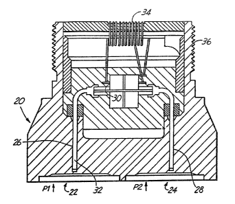
I~ FIG. 1, low~r hou~ng 20 Or a pressure
tran~ t~r ~ shown. In lower housing 20, two fluid
l~ol~tor 22, 24 roc~lYe pr~s~ure~ Pl and P2 ~pplled to
~h- tr~n~B~ttQr. Pa~s~gowAy~ 26, 28 in l~wer housing 20
co~n-ct isolators 22, 24 to pr~sure ~ensor 30.
Inc~mpr~s~ibl~ ~luid such 2~ on~ oil 32 fills
isolator~ 22, 24 ~nd passageways 26, 28 for coupling
pressur~ to fluid pr~ sur~ 3~nsor 30. Fluid pressure
fien~or 30 s~n~es pr~sur~ and provide~ ~n electrical
output iad~cat~e of pressure to connector 34.
Transm~tter circuitry in an upper housing (not shown)
WO92/17756 PCT/~'S92/0239~
210~3
-4-
which threadS on to the lower housing threads 36
receives the electrical output of sen~;or 30 and converts
it to an output which can be tranlsmitted over long
distances, such as a 4-20 mA output, or a digital
output.
In FIGS. 2 and 3, support block 40 is shown
having outer rim 42-surrounding flat faces 44, 4~ on
opposite sides. A cemtral passageway or hole 48 extends
between flat faces 44, 46. Support block 40 is bonded
to a diaphragm l~yer 50 (shown in FIG. 4) to support the
diaphragm layer. Support block 40 preferably has a
thickness "T" in the range of 3.8 m~ (0.~5 inch) to 10.2
mm (0.40 inch~. Thickness "T" of the support block is
selected to be about lO - 40 times the thickness of the
diaphrag~ layer to whiCh it i~ bonded, d2pending on
upper pressu~e lim~t for the ~nsor. Thickne~s ~'T" is
pr~fQrably more than 15 tim~ the thickne~s of the
diaphragm lay~r. Support block 40 is ormed of a
ceramic material sel~cted to have high stiffness with a
modulus of about 45 million pounds per square inch,
which is 2.5 times the ~tiffn~ss of silicon. A
prefer~ed high ~odulu5 cera~ic material for the support
~tructur~ eRdowed SR~SNn, o~ "SSNn, cera~ic ~aterial
suppli2d by ESK En~ineer~d Ceramics, Wacker Chemicals
USA Inc., Naw Canaan , . COnnQCt1CUt . This h~gh modulus
c~r~ic material ~xhibits bulk herm~ticity, and is
capablQ o~ ~orming hermetic ~als to other ~ater~als by
~al~ng proc~a8Q~ s~ch a~ ~rit soaling and active ~etal
brazing. Thi~ high ~odulus c~ramic ~aterial is also
30 electrically insulating. The el~ctrical in~ul~ting
propertie~ ~llow ~lectrically energized portions of a
~e~aæor, such ~s le~d~ and capacitor pl~tes, to closely
conSact support structtlr~ surf aces, without providing
W~9~17~56 PcT/~92/o2396
2 1 ~ 3
--5--
additional electrical insulating materials betwee~ the
support structure and a metal part to which the support
structure is ~ounted. Endowed SRBSN has a temperature
coefficien~ of expansion closely ~atched to that of
silicon. This allows hard, substantiall~ non-flexing
mounting of support block 40 to diaphragm layer 50
without added interm~diate layers, or resilient
materials, to relieve strain between adjacent surfaces
of materials of di~fering temperature coef~icients of
expansion. The ~atching expansion characteristics
reduce bo~h repeat la ~nd non-repeatable ther~al errors
over a wide ~e~perature rznge. Hysteresis in the sensor
output due to prQssure and temp~rature changes is
grQatly reduced. The c~ramic material selected
~ffectively co~bines de~irabl2 characteristics in a
single block of material and ~voids the problem of
~tacklng up multiple layers o~ dt ~ering materials to
o~taira de~red electrical insulating, bondirlg,
te~per~ture co~fic~erlt, aa~r~etic~ty and stiffrless
20p~operti~s~ The eff~cts of undesired stress ~rorn
tq~per~ture chang~s, line pr~urQ, dlffer~ntial
pres~ure and alountlng are controlled and the
construction o th~ ~ensor i~ si~ f ied bec~u~e the
ch~racto~i~t~c~ ar~ coDlbined ln a ~ingle ~Qaterial.
25In ~IG. 4, diaphragDI layer 50 i~ ~hown.
D~aphrag~ lay~r 50 ha~ a outer ri~ 52 surrounding layer
~lce S4 . A s~cond lay~r ~ace 56 (rlot ~ho m in F~G . 4 )
opposlte lay~r ~acæ i~ ~imilar to layer f~c~ 54. A thin
f~l~ m~tallization 58 i~ ~lectively deposited on a flat
30~ c~ oY l~y~r ~ac:e 56 betw~e2~ out~r r~m 52 and a
entral ~iaphr~g~ 60. Diapbragm 60 h~ a concave face
62 ~urxounded by an annul~r groove 64. The outer ri~ 52
o~ ~iaphrag~ l~yer 50 is ~pproximately the sa~e size as
W0~2/~77s6 ~T/US92~02396
2~0~4~3
-6-
the outer rim 42 of support block 44, the drawing in
FIG. 4 and FIGS. 2 and 3 having di~ferent scales to show
detail.
In FIG. 5, a sensor body 70 is shown formed of
a diaphragm layer S0 and two support blocks 40.
Circular capacitor plates 47 are formed of
metallizations deposited on faces 46 o~ support bloc~s
40~ The diaphragm layer 50 and 5upport blocks are
arranged in contact with one another as shown in FIG. 5
and the assembly is heated to a temperature o~ about
560 - 700 Centigrade. The metallizations 58 have a
thickness somparable to the surface roughness of faces
46 of the support blocks. A metallization o~ about 0.5
to 2.0 microns o~ aluminum is pre~err~d. Metalliz~tions
58 form ~ bond ~t the~ high temperatur~s to the faces
46 o~ th~ support blocks. The bond has a strength to
resist sop~r~tion o~ the blocks ~rom the sensor body 70
when th~ ~ensor is pressurized and al~o provides a fluid
s~al ~round diaphragm 60. In FIG. 5, central hole 48 in
each ~upport block 40 i~ co~ted with a metallization 72
to providQ an elactrically conductive path or sealed
f~edthrough b4twe~n fac~s 44, 46 o~ each block.
Cyl~n~rical ext~n~ions 74, 76 ~r~ ~e~ gly af~ixed to
~upport ~locks 44 with an active m~tal braze 78. The
active metal braze 78 r~sists separ~tion forces under
pr~ure, pro~idas a pre~surQ seal and ~l~o provides an
~l~c~rieal f~edthrough connection from metallization 72
to eo~nector tab 80. Diaphrag~ 50, which is formed of
doped silicon ~emiconductor material i~ ~lectrically
connected ~o connector ~ab 82 via m~t~llic tr~ck 84.
In FIG. 5, metal ~ittings 86, 88 are connected
to cylindrical extensions 74, 76 by ~raze j~int 90, 92.
The ~et~l fitting 86, 88 conn~ct to passa~eways 26, 28
WO9~56 PCT/~S92/02396
210~3
in lower trans~itter body 20 (FIG. 1) to couple isolator
Sluid, typically silicone oil, to cliaphragm 60. The
cylindrical ex*ensions provide electrical insulation
b~tween the feedthrough connecSions for the capacitor
plate (i.e. metallizations 72 and braze joints 78) ~nd
the metal transmitter body 20. The temperature
coef~icients of expansion of the metal fittings 86, 88
and cylindrical extensions 74, 76 wh~ch are ceramic can
be quite poorly ~atched because the braze joints 90, 92
are placed in co~pression when the parts shrink after
~razing. The arr~ngement with l~rger diameter ~etal
extension~ ~4 bonding around the periphery of a smaller
d1am~tQr ceramic cylinders 74, 76 avoids excessive
tensile forces in the ~er~ic material.
In FIG. 6, construction o~ a portion of
diaphrag~ 50 i5 shown in gre~ter d~tail. Metallization
58 i~ ~lectively deposited on flat peripher~l faces.
5h~ sur~ce o~ di~phr~gm 62 is concave and surrounded by
option~l grooves 64. Th~kne~ses o~ ~et~llization 58
20 and th~ c~pacltor plate 47 can be adjusted to provide
the desired spacing between c~pacitor plate 47 and
diaphrPg~ 50.
In FIGS. 7, 8, 9, alternate electrical and
pro~ure ~eedthrough ~rr~ngem~nts ~r~ ~hown. In FIG. 7,
an ~nnul~r moat ~00 i5 cut into a support block 40A to
providg ~trQs~ ~ell~f between ~etal coupling 86 brazed
to block 40A. S~parate ~QQdthrough holes 102, 104 are
provid~d for ~dthxough.connections for the cap~citor
plate 47 and diaphragm 50. Met~llization~ 106, 108 ~re
~ppl~ed ~o holes 102, 104 to co~plete connections
el~ctrically. ~etal t~bs 80, 82 ~re br~zed to support
block 40A to seal holes 102, 104.
Wo92t17756 PCT/US92/02396
2~483
-8-
In FIG. 8, a sensor body 110 is shown which
includes only a single-support block 40B rather than two
support blocks 4OA as shown in FIG. 7. Sensor body 110
is a gauge pressure sensor, and hasi a modified metal
fitting 86A brazed to it for connection to an isolator
~not shown).
In FIG. 9, a sensor body 112 i5 shown with a
square ceramic block 115 brazed to it to seal off an
electrical feedthrough far the associated capacitor
plate. In FIG. 9, a tube 114 is ~onnected to a ~upport
bloc~ 40C by braze ~oint 116 on the inside dia~eter of
hole 118 to provide fluid from an isolator to the
pres$ure s~nsing diaphragm.
The vari~tions ~hown in FIGS. 7, Z, 9 can be
~pplied to A s~nsor body such a~ sensor body 70 shown ln
FIC. S to adapt the invent~on to ~arious applications
and proces~ing equipment.
Although the pr~ent invention has been
d~scri~ed wi~h re~erence to preferred embodiments,
workers ~illed in ~he art will recognize ~hat changes
~y be ~de in ~orm and detail without departing from
the ~pirit and scope of the invention.