Note: Descriptions are shown in the official language in which they were submitted.
AIR COUPLED ULTRASONIC TRANSDUCER
Field of Invention
This invention relates to a generator and detector of ultrasound in air at
frequencies from audio to in excess of 600 kHz. More particularly this
invention relates to
an air coupled acoustic transducer which operates as a source and receiver up
to at least
2MHz.
Back, round of Invention
Electrostatic transducers for generating and detecting sound waves are well
known in the art and attention is directed to U.S. Pat. Nos. 3, 544,733;
3,946,422; 3,961,291;
4,329,547; 4,419,545; 4,908,805; 4,429,193; 4,439,642; 4,885,781; 4,993,072;
5,101,543;
4,809,355; 4,594,897; 4,855,783;4,558,184 and 4,593,567, which are typical of
known devices
and which generally include a moveable conductive material in juxtaposition to
a moveable
non-conductive dielectric material, both of which vibrate in unison. In most
instances a
conductive backplate in the form of a plate or foil is spaced from the
dielectric material _
which is usually a thin film of plastic such as a Mylar film. Between the two
there is an air
gap or space of predetermined thickness. The size and thickness of the air gap
is critical
and many attempts have been made to vary this gap by the use of multi
dielectric layers, and
spaces of varying types. The problem is that ultrasound is highly attenuative
in air above
1
s:l
Ps
;A
;,'. ,.,:! ... .. ... . ', ,'. '..'.. ..~~ r .. : . ,..,. .. '.: ...
" .. ....., . ......., .~''.,. ... ". . .
,..:.
.::
r
~ ~
..
.
J .
. .'..: ... :':,.
~
'.. . .. . ~'.'. ...'' ..,~.u.
';.. ' I,- ;. y . .
~ ~~ . . ...~ ':.,~. .. ;, . ~
.,':, .. '. ~
.
~.
~
.1 . . .
. ;.' .,
1. ,
1...~'. ~. .W.. ,
~.. - . . ;.: , ', , ~ . ;. , ..' . ~.. ',': . ." " .; . : _ : :..' ."'r
, : .' ..~. . :.: . ' . . '. . . : ' ' .. , ' .. ~ ;. ,
, o. ':~ . . .. .'n.. ,._ . ., ;.. . ~ . ~.~,~. . .': .. . . .. .
. ., -.. '., .. . ' .,
.
'
S. . . '... ' : ." . . .~~, .:,.~ ,.:' ~ ~ ;,.. .,..',. .. .
r~.~. '..,..'. ,
:,. ....:., .. '~.. ,'.'ayh, ~;_....
...,., .;,..'._.,,;'.. . , ...,'... .,. ',''' '. ~'. ' ,'. w , ~
:'.~. 'u,~'~.~~ '~.':v ,'; ; .'.
;'
W ;' ';: ~:
.
: :.
:
'
.
,
.
:.
.
; , r .
,.,
......,. .. ';. ..,,.,;:......' . '. ,. : , ' .,:. _. . ;~..;. ,,
...:.' ..'.~.'.; '~. ... , .,' . . ''.... ' , . .,:.'
~~~f~l~'~
about 600 kHz and conventional ultrasonic devices cannot adequately couple
vibrational
energy from solid to gas due to the large impedance mismatch. Use of
conventional
transducers for such applications as non-destructive testing of large planar
surfaces is greatly
hampered by the need to use an external coupling agent such as a gel. Many
prior art
patents rely on a simple air pocket between the dielectric material and the
backing electrode
so that the dielectric does not touch the backing electrode. Others, such as
U.S. Patent
4,908,805, support the dielectric membrane covering the backing electrode on
posts and use
glue to hold the membrane in place, and then provide openings in the
backplate. They are
designed for use at relatively low frequencies and the space taken up by the
glue is
effectively wasted space that could be used for generation of ultrasonic
energy. U.S. Patent
4,419,545 provides means for varying the area of the open holes in the
backplate leading to
the single air pocket in order to affect the frequency response and
sensitivity but the
vibrating element does not touch the back plate.
There is, therefore a need for improved acoustic transducers which can
operate efficiently at frequencies up to at least 2MHz, and it is believed
that this can be
attained by careful control of the surface roughness of the backplate so as to
provide a .
plurality of air pockets each of which vibrates. Such transducers would find
applications
testing large surfaces for internal flaws, among other applications obvious to
those skilled
in the art. Such other applications include human diagnostic and therapeutic
uses. As is
well known ultrasound, using a gel coupling agent, is used extensively for
medical puiposes.
.'.::
ll:.:.
y~ . .
Ob~iect of Invention
An object of the present invention is to provide efficient acoustic
transducers
which can operate in air up to frequencies of at least 2MHz, thereby
eliminating the need
for coupling liquids, gels or the like.
Brief Statement of Invention
By one aspect of this invention there is provided an acoustic transducer
operable in air up to at least 2MHz, comprising: a substrate having at least
one conducting
surface and having a plurality of pits of selected size and shape distributed
in a selected
pattern over at least one surface thereof;
at least one planar dielectric film superimposed over said substrate so as to
provide
a plurality of air pockets between said substrate and said dielectric film;
and
a planar conducting upper electrode superimposed on said dielectric film.
By another aspect of this invention, there is provided an acoustic transducer
operable in air up to at least 2MHz, comprising a substrate having at least
one conducting
surface;
at least one dielectric film, having a plurality of pits of selected size and
shape , .
distributed thereover in a selected pattern, superimposed over said substrate
so as to provide
a plurality of air pockets between said substrate and said dielectric film;
and
a conducting upper electrode superimposed on said dielectric film.
3
By yet another aspect of this invention there is provided a method for
producing an acoustic transducer operable in air up to at least 2MHz,
comprising:
(a) producing a selected pattern of pits in a planar surface of a conducting
substrate;
(b) superimposing said pitted surface with a film of dielectric material so as
to
trap air into a plurality of said pits; and
(c) superimposing a planar conducting electrode over said dielectric film.
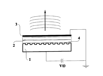
Brief Description of Drawines
Figure 1 is a schematic cross sectional view of one embodiment of the present
invention.
Detailed Description of Preferred Embodiments
Commercially available ultrasound devices for use beyond about 600kHz
generally rely upon using solid piezoelectric elements, which may be embedded
in a polymer
's
matrix, which is formed in the shape of a thin disk. Electrodes are placed on
each side of
the disc so that an electric field can be applied to the piezoelectric
elements and excite them
into vibration. The polymer matrix serves both to decrease the acoustic
impedance from
that of a solid and to dampen the vibrations of the inherently resonant
elements. in order
., ,
~rJ .. '~ .;. ~ '-. .. : ' ' ':~ ~ ' .. ,.. ., ..
to transfer a measurable degree of acoustic energy to the air, it is usually
necessary that one
side of the disc be loaded only by air (a so-called air backed transducer)
while applying a
thin impedance matching layer to the other face ( a so-called 1/4 wave
matching layer).
Such devices are capable of reaching operational frequencies of about 5 MHz,
but their
sensitivities are low, and they are often resonant devices in order to get
useable output,
which means that they can only be operated at a single well defined frequency
of design. ~
In contrast the capacitance devices of the present invention have an order of
magnitude greater sensitivity in detection and generation than the
piezoelectric air-coupled
transducers described above. This means that in any practical ultrasonic
system two orders
of magnitude greater sensitivity result as a source and a receiver are
necessary and the
effects are cumulative. Furthermore, as the devices of the present invention
are not
resonant devices they can be run at any frequency up to and including the
bandwidth limit.
As can be seen from Figure 1, the devices of the present invention are an
extension of sonic devices known as electrostatic speakers and microphones
which comprise
three basic components: namely a rigid conducting backplate 1, preferably
planar, a thin
dielectric layer 2 superimposed thereon and a thin conducting upper electrode
3. The rigid
backplate 1 is provided with random surface contours 4 on one side produced
by, for
example, roughening with sandpaper. The surface contours serve to introduce
air pockets
between backplate 1 and the dielectric layer 2. The dielectric layer allows
electrical
isolation between backplate 1 and upper electrode 3. When a voltage is applied
across the
F,~~~ ' '.". :,'.,. .. ,..... ' . ,. .:..~. , , ,: .. ~: ~ . .~.: ' .., .,.~.
.. '.''.. ,,.
.
. .
.
.
'
'
'
:. : .. ,
,.
.
.n ,,. ,.
:.:
-. " :.. .. ;
.. ' .y'~...' '.....:..'".. .",. ., ',
. ~ ~.'. .~ , '-
.
.
,
. .. i . t
.. .. , y ..
, '.
;. ..
:
~
'
~ s
i
;
_.,
:. :.
.:. .
,
. .
. ,i~ .: ~.. .., : ~:~:
.l; ~
,
..
..
. ~
.
, '
.
~
s
'
~~
'.
.
~
,
. '
,
.. .
.
.
,
;
.
.
...,"..
.. .,'.
. ,
~. >
...
: .
.:
'.
~
..
p_... ,,.
. ,., ,..... ~' :~. ~.,
' :; .
.
.:.'...,.. .~.'.. ..~ . v ".. . .".
.'.. '. ....'.~ :
'.. . :'.. .. .. ~ ..~ . ..y. ,:...." ~ :., :.~',' ~~...~~ '., ...,.
,. .;...~ . ~...:. ..::~.',.:., .,;'.;, ', , ~. .
,. . ' . . . . ,' , . ~ . . ' '
~~.v:~t~~
backplate and upper electrode an electromagnetic pressure results at the upper
electrode
3 which drives it into motion. This motion is tailored and enhanced by the
vibrations of the
air pockets trapped beneath the dielectric layer 2 in the surface contours 4
of the backplate
1. In most microphones the dielectric layer 2 is a metalized electret such as
a Mylar~,
Kapton~ or Teflon~ film which markedly increases the signal strength due to
charging
processes associated with electret materials. Commercial microphones based on
the above
construction operate at frequencies up to about 200 KHz. Commercial range
finders also
exist which can generate frequencies of similar magnitudes.
By carefully controlling the roughness of the backplate 1 by using selected
grades of sandpaper and selecting the dielectric layer 2 and upper electrodes
from
metallized, electret, polymer films it is possible to raise the frequency
response to 600-800
KHz with small resonant responses as high as 1.5 MHz. It does not, however,
appear ~ w , ,
possible to raise frequencies higher by these techniques because above about
600kHz the
emergent ultrasonic beam breaks up into many smaller beams, leaving the
transducer
uncharacterizable. Without wishing to be bound by this theory, it is believed
that this is a
function of the irregular and non-uniform nature of the roughening process
used to create
the air pockets in the backplate 1 and variations in the dielectric
properties. That is to say,
the varied size, distribution, and shape of the air pockets causes the
frequency response and
sensitivity to vary across the face of the device. Since the air pockets are
so small it is
believed that conventional mechanical production of the surface contours on
the backplate
6
~~~~i;~~
1 is unlikely to produce the uniformity necessary to produce well
characterized capacitive
transducers at MHz frequencies.
It is believed that the necessary uniformity can be achieved by employing
integrated circuit (IC) techniques in the production of the backplate.
Anisotropic etching
of a glass, silicon or semi conductor substrate can be effected so as to
provide very uniform
air pockets having dimensions in the range of microns to tens of microns both
deep and
wide. Silicon wafers are particularly suitable substrates as they are readily
available in
thicknesses between about 25~c and SOO~,m, are readily etchable by standard
techniques and
their purity and "perfect" crystalline properties will allow the necessary
uniformities.
The dielectric film or films (preferably Mylar~ or Kapton~ but also including
piezoelectric polymer films) may be adhered to the etched silicon wafer by any
conventional
means which may include heat and usually without the need for an adhesive. The
dielectric
films may also be spun cast onto the substrate from solution in known manner.
The spin
casting technique is particularly suitable for use with polyimide films.
A metallic upper electrode may be deposited on the surface of the dielectric
film by vapour phase deposition or other conventional techniques, such as
sputtering.
Alternatively, it may be possible to use a substantially smooth backplate and
provide an etched polyimide or other dielectric film.
It will be appreciated that for certain applications the depth of the etch
pits
in either the substrate or the dielectric film, as the case may be, may extend
completely
7
,'.. ,
through the substrate or film.
Example 1
Preparation of Silicon Backplates by Anistropic Etchins
250~.m thick silicon wafers having masking layers of Si3 N4 (--100A) and Si)2(-
-80A)
were obtained from Virginia Semi Conductor Inc., Fredericksburg, VA. A
photoresist layer
(Microposit Developer Concentrate Shipley FK059-021085 sold by Shipley
Company,
Marlboro MA) was poured onto the surface of the masked silicon wafers and spun
at 3,500
rpm for 60 seconds. The coated wafers were then baked at 90°C for 30
minutes. A mask
comprising a piece of glass with a metallic coating from which an array of
40~em diameter
circles at 80~cm between centres had been removed, and manufactured by
Precision
Photomask, was placed over the baked photoresist. The baked photoresist and
mask were
then exposed to UV light of intensity 1.5 mW/cm'- for at least 11 minutes, and
developed
in a 1:1 solution of Microposit Developer Concentrate Shipley FK059-021085.
(Shipley
Company) for 25-30 seconds; to remove the exposed circles of the photoresist
and reveal an
array of Si02 circles surrounded by photoresist. .
The developed wafers were then baked at 135°C for 30 minutes and the
exposed SiO,
circles were etched using buffer HF (10 volume NH4 and 1 volume HF): The Si3
N4 circles
were then etched using refluxed boiling 85% phosphoric acid at 170° for
about 30 minutes.
This revealed an exposed array of bare silicon circles which were then etched
using aqueous
g
. ; . ; ., .'
~ a; . , .
.:;: . . '
: , ,
- .
'
'
~ . ,; ., " , .: ; : .. , ;;.
. , . , : -.: . . ;.,
... .. :.' . :
:: :. , _ .
_ - .
.
. :z
r;: , : '' ~ :
.; . ~'
r
,
'~
, ;: , ~ : . .;
, :. : : - ,,
~ . ,;
:. .
.
~
'
: . : ' . : ; . :. . . ,
:: ,. ' . . ; : ,.,
;., ~;, ,.
' , , ~
'
:.. : , , ; ,, . . : ' . ..
,
, .
:, ; , .: ";. , . ; ;,.
~~t~~~:~!~ r
44% KOH for 50 minutes. The KOH etchant is an anisotropic etchant for silicon
producing
pits hexagonal in shape at the surface and up to about 30um deep. After
chemical etching,
residual photoresist was removed by boiling in concentrated HZ SO4 or by
immersion in
Shipley 1165 photoresist remover for 3 minutes.
At this stage a 1000 A thick gold film was evaporated onto the side of the
wafer
containing the pits to provide one electrode of the capacitor. It will, of
course, be
appreciated that heavily doped or selectively doped silicon wafers could
equally well be
employed for affecting etching or to provide electrode arrays or potential
aperturing and,
using similar standard etching techniques, backing plates with selectively
arranged pits can
be produced.
Example 2
Preparation of Dielectric Laver and Upper Electrode
Premetallized thin dielectric films are commercially available. Particularly
suitable
for the purposes of the present invention are S~m Kapton and Mylar films
having a thin
0100-1000A) aluminum layer evaporated on one surface thereof. An etched
backplate
produced as in Example 1 and a Kapton film were cleaned by blowing with
compressed air
to remove dust. The film was then superimposed on the etched surface of the
wafer while
applying a voltage of about SOV across the backplate and upper electrode to
help eliminate
some of the trapped air by sucking the film tightly against the backplate. In
conjunction
9
~.~.~~2~ ~~'
with the applied voltage, gentle rubbing of the surface of the upper electrode
with a soft
tissue may be effected to remove excess trapped air. Once in place the film is
held in place
by mechanical means such as to prevent subsequent re-introduction of air into
the planar , ,
area between film and backplate.
Example 3
Preparation of Dielectriclaver and Unver Electrode by LC. Processin
;,
An etched silicon wafer was prepared as in Example 1. A diluted adhesion
promoter
~,
:(QZ3289 and QZ3290 - Ciba Giegy) was spun on the surface at 5000 rpm for 30
seconds.
A Sum polyimide film (Probimide 200 from Ciba-Geigy) was spun onto the
prepared surface
at 3700 rpm for 50 seconds, and then baked at 89° C for 30 minutes,
plus 150°C for 15
minutes and 240°C for 15 minutes. A final high temperature cure at
300°C-400°C for 1
hour minutes can be applied to cross link the polyimide. Once the film had
been cured a
metal electrode, such as aluminum or gold, was deposited on the surface by
vapour phase
deposition to a thickness between 500 - 2000A; preferably 1000A.
It will be appreciated that while this invention has been described with
particular
reference to operating: in air, the devices of this invention can also be
operated in a liquid
such as water. 1n such a case it is preferred that an additional thin plastic
film be provided
over the upper electrode so as to prevent oxidation. Devices operating in
water provide a
:a simple means for producing a standard ultrasonic transducer having a well
characterized
,y
to
..,
'.,
,:
. r,
. ' .:. .y' ;'. ~:. . , ~-y ,. . .. ..: ,. ~. - - v: :.: , ::
~~.i~~~~'~
beam profile for calibrating other devices such as piezoelectric tranducers.
11
. ' .,.; ,.. ,~'..:,. n ~:'... . .r ' ...., . , ;..:. ' ' .. '
' . '~. . ~ ~. ..._: ~ ,. ..; ... ~ ...
. ~
-
. . . ~.~''..~~~.
. ,. . '.~,,..: . ~. , . . :_.,. ..... .. ''';~~....
.. ~'' . ~:'.:' ~. .';. . '. '. ....... '
: '...,-' ' ., ~~.w .
' . ~ ..
,... ,." ,. , _.. . .'...:' : .. , ~;~.~.
' .., ~ . .
.. , .. ,..'.' ~ ,..,~.,.: ; . ;:....: _ . W ~ ";,.:.: n:
... ..,':..'. ' '". ':.. ~. .' '. . : ,. ' _ 'v.,n: ., '.: .
.' .' ' '
;.,,. .~..
.'..
. . - . .
''
' ' , ,
'. . . :; ~ ' ..._ . ' .
Y ..
,
i
_ . ... , . ' . ,
..
. .
l .'. , . .. , _ ' , : . .' ~ : , '.. , : ' . . ; ~, ' .' '
~. , ' . ' ~.. ,. ... : ~.. . ..~''. ', ~:vq.
~
.