Note: Descriptions are shown in the official language in which they were submitted.
Wt~ .92/ 16142 PCT/L)S92/Ot 89a
21~~~fi~1
L01I NOI6E OPTICAL PR08E
TECHNICAL FIELD
The present invention relates to the sensing of
energy. More specifically, the present invention relates
to the reduction of noise in signals via an improved
sensing mechanism.
WO 92/16142 PCT/US92/0189.1
2
BACKGROUND ART
Energy. is often transmitted through or reflected from
a medium to determine characteristics of the medium. For
example, in the medical field, instead of extracting
material from a patient's body for testing, light or sound
energy may be caused to be incident on the patient's body
and transmitted (or reflected) energy may be measured to
determine information about the material through which the
light has passed. This type of non-invasive measurement
is more comfortable for the patient and can be performed
more quickly.
Non-invasive physiological monitoring of bodily
function is often required. For example, during surgery,
blood pressure and the body's available supply of oxygen,
or the blood oxygen saturation, are often monitored.
Measurements such as these are often performed with non-
invasive techniques where assessments are made by
measuring the ratio of incident to transmitted (or
reflected) light through a portion of the body, for
example a digit such as a finger, or an earlobe, or a
forehead.
Transmission of optical energy as it passes through
the body is strongly dependent on the thickness of the
material through which the light passes, or the optical
path length. Many portions of a patient's body are
typically soft and compressible. For example, a finger
comprises skin, muscle, tissue, bone, blood, etc.
W~' 92/16142 PCT/US92/01894
21(1J6~~.
Although the bone is relatively incompressible, the
tissue, muscle, etc. are easily compressible with pressure
applied to the finger, as often occurs when the finger
moves., Thus, if optical energy is made incident on a
finger and the patient moves in a manner which distorts or
compresses the finger, the optical path length changes.
Since a patient generally moves in an erratic fashion, the
compression of the finger is erratic. This causes the
change in optical path length to be erratic, making the
absorption erratic, resulting in a~difficult to interpret
measured signal.
Many types of non-invasive monitoring devices have
been developed to try to produce a clear and discernable
signal as energy is transmitted through a medium, such as
a finger or other part of the body. In typical optical
probes a light emitting diode (LED) is placed on one side
of the medium while a photodetector is placed on an
opposite side of the medium. Many prior art optical
probes are designed for use only when a patient is
,. relatively motionless since, as discussed above, motion
induced noise can grossly corrupt the measured signal.
Typically, probes are designed to maximize contact between
the LED and the medium and the photodetector and the
r
medium to promote strong optical coupling between the LED,
the medium, and the photodetector, thereby generating a
strong. output signal intensity. In this way, a strong,
clear signal can be transmitted through the medium when
the patient is generally motionless.
WO 92/16142 PCT/US92/01894
~1U5b8.~. 4
For example, U.S. Patent No. 4,880,304 to Jaeb, et
al. discloses an optical probe for a pulse oximeter, or
blood oxygen saturation monitor, comprising a housing with
a flat lower face containing a central protrusion in which
a plurality of light emitting diodes (LED's) and an
optical detector are mounted. When the probe is placed on
the patient's tissue, the protrusion causes the LED's and
the detector to press against the tissue to provide
improved optical coupling of the sensor to the skin. In
another embodiment (Figures 4a and 4b in the Jaeb patent),
the LED's and the detector are arranged within a central
chamber, generally horizontal with respect to the tissue
on which the probe is placed. A set of mirrors or prisms
causes light to be directed from the LED's onto the tissue
through a polymer sealant within the chamber, the sealant
providing a contact with the tissue for good optical
coupling with the tissue.
U.S. Patent No. 4,825,879 to Tan, et al. discloses an
optical probe wherein a T-shaped wrap, having a vertical
stem and a horizontal cross bar, is utilized to secure a
light source and an optical sensor in optical contact with
a finger. The light source is located in a window on one
__
side o~ the vertical stem while the sensor is located in
a window on the other side of the vertical stem. The
finger is aligned with the stem and the stem is bent such
that the light source and the sensor lie on opposite sides
of the finger. Then, the cross bar is wrapped around the
finger to secure the wrap, thereby ensuring that the light
Wf~ 92/16142 PCT/US92/01894
~~Oa681
source and the sensor remain in contact with the finger to
produce good optical coupling.
U.S. Patent No. 4,380,240 to Jobsis, et al. discloses
an optical probe wherein a light source and a light
detector are incorporated into channels within a slightly
deformable mounting structure which is adhered to a strap.
Annular adhesive tapes are,placed over the source and the
detector. The light source and detector are firmly
engaged with a bodily surface by the adhesive tapes and
pressure induced by closing the strap around a portion of
the body. An alternative embodiment provides a
pressurized seal and a pumping mechanism to cause the body
to be sucked into contact with the light source and
detector.
U.S. Patent No. 4,8b5,038 to Rich, et al. discloses
an optical probe having an extremely thin cross section
such that it is flexible. A die LED and a die
photodetector are located on a flexible printed circuit
board and encapsulated by an epoxy bead. A spacer, having
circular apertures positioned in alignment with the LED
and photodetector, ~is placed over the exposed circuit
board. A transparent top cover is placed over the spacer
_ .
and is~'sealed with a bottom cover placed under the circuit
board, thereby sealing the probe from contaminants. A
~ spine may be added to strengthen the device. The
flexibility of the device allows it to be pinched onto the
body causing the epoxy beads over the LED and the
photodetector to protrude through the apertures in the
WO 92/16142 PCT/US92/0189~1
spacer and press against the top cover such that good
optical contact is made with the body.
U.S. Patent No. 4,907,594 to Muz discloses an optical
probe wherein a dual wall rubberized sheath is fit over a
. finger. A pump is located at the tip of the finger such
that a pressurized chamber may be formed between the two
walls, thereby causing an LED and a photodetector located
~~ in the inner wall to be in contact with the'froger.
Each of the above described optical probes attempts
to cause a strong measured signal at the photodetector by
optimizing contact between the LED, the patient, and the
probe. However; this optimization forces compressible
poxtions of the patient's body to be in contact with
surfaces which compress these portions of the patient s
body when the patient moves . This can cause extreme
changes in the thickness of material through which optical
energy passes, i.e., changes in the optical path length.
Changes in the optical path length can produce enough
distortion in the measured signal to make it difficult or
impossible to determine desired information. Thus, a need
exists for a probe which inhibits motion induced noise, or
motion, artifacts, during measurement of a signal while
still generating a transmitted or reflected signal of
sufficient intensity to be measured by a detector.
W~ 92/16142 PCT/US92/01894
SUI~1ARY OF THE INVENTION
The present invention is a probe for use in both
invasive and non-invasive energy absorption (or
reflection) measurements. A base is formed in a shape
generally corresponding to the material on which
measurements are to be made, for example, a section of a
patient's body. such as a finger, an earlobe, a forehead,
a toe, an organ, or a portion of tissue. The base has a
forward end, a rear end, a top and a bottom. An aperture
is formed in the top of the base. The aperture is the
entrance to a chamber: A detector, such as a
photodetector, is mounted within the chamber, typically in
_ the bottom of the chamber. The material on which
measurements are to be made is placed on the base such
that any compressible portion of the material is located
directly adjacent the chamber. Thus, the compressible
portion of the material is caused to rest above or enter
into the chamber. The chamber is deep enough that any
material which intrudes into the chamber does not contact
anything which might cause compression.
A light source, such as an LED, is affixed to the
_ .
material, opposite the photodetector. The LED emits light
energy which propagates through and is absorbed by the
~ material along tha optical path length, or thickness of
material through which light propagates. An attenuated
light energy_signal emerges from the material, into the
chamber. As light propagates through the material, it is
WO 92/i6142 PCT/US92/0189.~
210~b81
scattered by the material and is thus transmitted into the
chamber over a broad range of angles. The photodetector
produces an. electrical signal indicative of the intensity
of the signal transmitted by the material. The electrical
signal is input to a processor which analyzes the signal
to determine information about the medium through which
light energy has been transmitted.
The probe of the present-invention does not make
direct physical contact between the photodetector and the
material. Even though this results in less than optimal
optical coupling, and thus generally lower output signal
intensity, it enables an easily compressible portion of
the material that light energy passes through to rest in
the chamber and not be compressed. This results in less
disturbance of the optical path between the light source
and the detector. Since the LED is generally aligned with
the chamber and the photodetector, the light energy signal
propagates through the portion of the material which rests
above or is accommodated within the chamber. The chamber
R
allows the compressible portion of the material to remain
substantially uncompressed, even during motion, since
nothing within the chamber physically contacts the
materiel through which light energy passes to cause
compression. Thus, the thickness of the material, or the
optical path length, is stabilized, thereby improving the
signal-to-noise ratio of the measured signal. The
intensity of the signal received at the photodetector may
be improved by emission of higher intensity light by the
W(192/1614? PCT/US92/0189a
9
'~~,~.~~~~1
LED to compensate for losses caused in the chamber and by
the poor optical coupling. Thus, the probe of the present
invention produces a strong, clear signal wherein noise
' _ due to motion, or motion artifacts, is substantially
reduced.
In another embodiment of the invention, an LED may be
mounted within the chamber, typically at the bottom of the
- chamber. A material is placed over the probe, and a
photodetector is affixed to the material, opposite the
chamber. The chamber still functions to protect easily
compressible portions of the material through which light
energy will pass from being compressed, even during
motion. Another embodiment having the LED within the
chamber is one in which a collimating lens assembly is
also incorporated into the chamber. The lens assembly is
located deep enough within the chamber that any portion of
the material on which measurements are being made that
penetrates into the chamber does not contact the lens
assembly. The collimating lens assembly causes light from
a
the LED to be focused on the material above the chamber,
thus providing a less scattered signal transmitted into
the chamber and onto the photodetector surface, thereby
util'izi~ng the photodetector more effectively.
In yet another embodiment of the present invention,
a photodetector is mounted within the chamber, typically
at the bottom of the chamber. A material is placed
adjacent the probe and an LED is affixed to the material,
opposite the chamber. A light collecting lens is placed
CA 02105681 2002-10-22
within the chamber, above the photodetector, leaving enough
space within the chamber for any easily compressible
material to intrude into the chamber without contacting the
lens and being compressed. The lens collects light which has
been scattered by the material and directs this light onto
the surface of the photodetector, resulting in a stronger
measured signal.
In one preferred embodiment there is provided a sensor
comprising: a housing having a support surface for a
material which is to be analyzed; a chamber having an
entrance in the form of an aperture positioned on said
housing support surface such that said material covers said
aperture and is supported by said support surface around
said aperture; and a detector located in said chamber for
detecting energy or light which has passed through a portion
of said material and enters said chamber through said
aperture, said detector positioned in said chamber in a
manner such that said portion of said material which covers
said aperture is isolated from contact with any surface
which could cause compression of said portion of said
material such that said portion of said material remains
substantially uncompressed.
In another preferred embodiment there is provided in an
apparatus for sensing light absorption through
transillumination of flesh by a light source and reception
of light by an optical detector, a sensor comprising: a
base having a support surface for supporting a portion of a
body member; a chamber having an entrance in the form of an
aperture on said base support surface such that said portion
i
CA 02105681 2002-10-22
10a
of a body member covers said aperture and is supported by
said support surface around said aperture; and a detector
located in said chamber for detecting light which has passed
through said portion of a body member and enters said
chamber through said aperture, said detector positioned in
said chamber in a manner such that said portion of a body
member which covers said aperture is isolated from contact
with any surface which could cause compression of said
portion of said body member such that said portion of said
body member remains substantially uncompressed.
In a further preferred embodiment there is provided a
method for acquiring a signal comprising the steps of:
transmitting energy into a material; locating said material
adjacent an aperture formed in a base wherein said aperture
leads to a chamber, such that said base, aperture, and
chamber cooperate to support said material in a manner that
a portion of the material immediately adjacent and covering
said aperture remains substantially unperturbed; and
receiving an attenuated signal at a detector within said
chamber, said detector being recessed from said material.
The invention also provides a probe for measurements of
a signal which has been attenuated by a compressible
material, comprising: a base; an aperture formed in said
base; a chamber extending from said aperture into said base,
said chamber being placed directly adjacent the compressible
material, the chamber, base, and aperture cooperating such
that a portion of the compressible material adjacent said
aperture remains generally uncompressed while a portion of
CA 02105681 2002-10-22
lOb
the compressible material surrounding said aperture is
supported by said base; and a detector positioned within
said chamber in said base, said detector being disposed to
receive energy which has travelled through a portion of said
material, or an energy source positioned within said chamber
in said base for transmitting energy into the material.
W(~ 92/16142 PCT/US92/01894
m ~:~.~~~1
BRIEF DESCRIPTION OF THE DRAWINGS
FIG. 1 illustrates a schematic medium comprising N
' . different constituents.
FIG. 2a illustrates an ideal plethysmographic signal
,
that would be measured by the optical probe of the present
invention when utilized for pulse oximetry.
FIG. 2b illustrates a realistic signal measured by
the optical probe of the present invention when utilized
for pulse oximetry.
FIG. 3 is a perspective view of a probe of the
present invention having a single segment chamber.
FIG. 4 is a cross-sectional view of an optical probe
of the present invention illustrating a single segment
chamber having a detector within it.
r
FIG. 5 is a cross-sectional view of a probe of the
present invention having a detector resting on a shell of
base material.
FIG. 6 is a cross-sectional view of a probe of the
present invention incorporating a Light collecting lens.
WO 92/16142 PCT/US92/0189.~
I2
FIG. 7 is a cross-sectional view of a probe of the
present invention illustrating a single segment chamber
having an LED within it.
FIG. a is a cross-sectional view of a probe of the
present invention incorporating a collimating lens
assembly.
FIG. 9 is a cross-section view of a probe of the
present invention wherein the LED and the detector are not
aligned along the central axis of the chamber.
FIG. 10 is a perspective view of another embodiment
of a probe of the present invention having a two segment
chamber:
FIG. 11 is a cross-sectional view of another
embodiment of the probe of FIG. 10 incorporating a two
segment chamber having a detector within it.
FIG. 12 is a cross-sectional view of another
embodiment of the probe of FIG. 10 incorporating a light
_ r
collecting lens in a two segment chamber.
FIG. 13 is a perspective view of probe of the present
invention having a three segment chamber.
WO 92/16142 PCT/US92/01894
13 . ~~~~~81
FIG. 14 is a cross-sectional view of the probe of
FIG. 13 incorporating a three segment chamber having a
detector within it.
FIG. 15 is a cross-sectional view of another
embodiment of the probe of FIG. 13 incorporating a light
collimating lens.
FIG. 16 is aperspective view of a probe of the
present invention specifically designed to be used with a
digit.
FIG. 17 illustrates a schematic finger comprising
fingernail, skin, bone, tissue, muscle, blood, etc.
FIG. 18 is a cross-section view of the probe of FIG.
16.
FIG. 19 is a longitudinal cross-sectional view of the
probe of FIG. 16.
FIG. 20 is a cross-sectional view of another
embodiment of the probe of FIG. 16 incorporating a light
collecting lens.
FIG. 21 is a cross-sectional view of a probe of the
present invention designed to be utilized for reflectance
measurements.
WO 92/16142 PCT/US92/0189.~
z~o~s~2 ~4
FIG. 22 is a cross-sectional view of a probe which is
advantageously used for non-invasive measurements when a
material is,compressible on more than one side. The Drobe
has two bases, each with a chamber to house a detector or
an energy source and thereby reduce motion artifacts.
FIG. 23 is a cross-sectional view of a probe having
a generally cone-shaped chamber with a reflective surface
which advantageously causes energy,to be concentrated, or
"funneled", onto the surface of a detector within the
chamber, improving the measured signal.
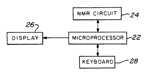
FIG. 24 is a schematic of one system which may
advantageously employ a probe of the present invention.
Wi) 92/16142 PCT/LJS92/01894
~I0~681
DESCRIPTION OF THE PREFERRED EMBODIMENT
Examination of a material is often advantageous,
' . especially when it is difficult or expensive to procure
and test a sample of the material. For example, in
physiological measurements, it is often desirable to
monitor a patient without unnecessary extraction of blood
or tissue.- The known properties.of energy absorption as
energy propagates through a material may be used to
determine information about the material through which the
energy has passed. Energy is made incident on a material,
and a measurement is made of energy either transmitted by
or reflected from the material.
The amplitude of the measured signal is highly
dependent on the thickness of the material through which
the energy gasses, or the optical path length. A
schematic medium 20 comprising N different constituents A~
through A~ is shown in Figure 1. Energy transmitted
through the medium 20 is approximately attenuated
according to the equation:
IsIQe F'~ 1ltCtJCt
(1)
where e; is the absorption coefficient of the itn
constituent: xi is the thickness of the ith constituent
through which light energy passes, or the optical path
length of the ith; and ci is. the concentration of the itn
constituent in thickness xi.
WO 92/16142 PCT/US9210189.1
~1~~68~. is
Since energy absorption is strongly dependent on the ,
thicknesses of the constituents A~ through AN which make up
the medium .20 through which the energy passes, when the
thickness of the medium 20 changes, due to motion for
example, the thicknesses'of the individual constituents A~
through Aw change. This causes the absorption
characteristics of the medium 20 to change.
Often a medium 20 is under random or'erratic motion.
For example, if the medium 20 is an easily compressible
portion of a patient's body and the patient moves, the
medium 20 compresses erratically causing the individual
thicknesses X~ through Xw of the constituents A~ through AN
to vary 'erratically. This erratic variation may cause
large excursions in the measured signal and can make it
extremely difficult to discern a desired sicrnal, as would
be present without motion induced noise, or motion
artifacts.
For example, Figure 2a illustrates an ideal desired
signal waveform, labelled Y, measured in one application
of the present invention, namely pulse oximetry. Figure
2b illustrates a more realistic measured waveform S, also
measured in a pulse oximetry application, comprising the
_ .
ideal desired signal waveform Y plus motion induced noise,
n, i.e. S=Y+n. It is easily seen how motion artifacts
obscure the desired signal portion Y.
Figure 3 is a perspective view of an optical probe
100 of the present invention which greatly diminishes the
effects of motion artifacts on the measured signal.
W(~ 92/16142 PCT/US92/01894
1?
Figure 4 shows a cross-sectional view of the optical probe
100 of the present invention taken along line 4-4 in
Figure 3. For clarity in the perspective view of Figure
3, a material 128 on which measurements are to be taken is
not shown placed adjacent the probe 100. However, the
material 128 on which measurements are to be made is shown
w
in Figure 4. Referring to Figures 3 and 4, a base 110,
having a top 112, a bottom 114, a forward end 116, and a
rear end 118, is made of a material which is preferably
rigid and opaque. It will be understood, however, that
the probe 100 may be made of materials which may be rigid,
resilient, opaque, or transparent, for example.
An aperture 120 is formed in the top 112 of the base
110: Typically, the aperture 120 is located at a point
between one-quarter and one-half of the length of the base
100. The aperture 120 may be of any shape, including but
not limited to circular, square, or triangular. The
aperture 120 forms the opening to a chamber 122 which may
also be of any shape. A lateral cross-section (not shown)
of the chamber 122 is typically the same shape as the
aperture. A central axis 124 of the chamber 122 is
defined by a line aligned perpendicular to the aperture
_ ,
120 and extending generally through a central portion of
the aperture 120.
A light source 130, typically a light emitting diode
(LED), is affixed to the material 128, aligned along the
central axis 124 of the chamber 122 opposite the chamber
122. Typically,. an adhesive such as medical tape is used
WO 92/16142 PCT/US92/01894
21Q7681
18
to affix the LED 130 to the material 128. A detector 126,
such as a photodetector, is placed within the chamber 122.
A central portion of the photodetector 126 is generally
. aligned with the central axis 124 of the chamber 122,
typically at the bottom 114 of the chamber 122. The
photodetector 126 may be fixed within the chamber 122
according to a number of different methods, including but
not limited to adhesive, a press fit, or clear epoxy resin
which transmits light over a range of wavelengths of
interest. Typically, no matter how the photodetector 126
is held within the chamber 122, the bottom surface 114 of
the chamber 122 is made opaque either via the press fit or
via paint or tape, for example.
It is often the case that materials 128 on which
absorption measurements are performed are, at least in
part, easily compressible. Any easily compressible
portion of the material 128 is placed directly adjacent
the chamber 122. The area surrounding the aperture 120
supports the material adjacent the chamber 122. The
chamber 122 is wide enough that any compressible portion
of the material 128 located above the aperture 120 may
intrude into the chamber 122. Thus, the material 122 may
rest abbve or penetrate slightly into the chamber 122 and
is thereby shielded from perturbations which compress the
material 128, such as pressure caused when the material
128 is touched.
The chamber 122 is deep enough that the photodetector
126 and the bottom 114 of the chamber 122 do not come into
WO 92/16142 PCT/US92/01894
I9
~~~~~$~.
contact with the easily compressible portion of the
material 128, even when the material 128 is caused to
move. Thus, along the central axis 124 of the chamber 122
nothing comes into physical contact with the easily
compressible portion of the material 128 and causes it to
compress. With little or no compression of the material
128 in this region, the thickness~of the material 128, or
the;..: ,optical ;, path length , of light energy propagating
through the material 128, is substantially stabilized.
The LED 130 emits light at a known wavelength. The
light propagates through the material 128 and an
attenuated signal is transmitted into the chamber 122 to
be received by the photodetector 126. As light from the
LED 130 propagates through the material 128, it is
scattered by the material 128 and is thus transmitted into
the chamber 122 over a broad range of angles. Thus, some
of the light is caused to be incident on the opaque walls
123 of the chamber 122 and is absorbed. Although the
signal travels through a greater optical distance to reach
the photodetector 126 at the bottom 114 of the chamber 122
than if the photodetector 126 were immediately adjacent
the material 128, thus eliminating direct coupling between
the p3~Q~odetector 126 and the material 128, the resulting
degradation to signal intensity is compensated for by the
stabilization of the optical path length and the resultant
reduction of noise in the measured signal. The
photodetector 126 produces an electrical signal indicative
of the intensity of light energy incident on the
WO 92/16142 PGT/US92/01894
photodetector 126. The electrical signal is input to a
processor which analyzes the signal to determine
characteristics of the media 128 through which the light
energy has passed.
Additionally helping to improve signal quality, the
opaque quality of the base 110 absorbs ambient light which
can interfere with the signal measured at the
photodetector 126. Further, the opaque bottom 114 of the
chamber 122 protects the photodetector 126 from ambient
light which can obscure the desired signal measured at the
photodetector 126. Thus, an accurate measurement of the
intensity of the attenuated signal may be made at the
photodetector 126.
An alternative embodiment of the chamber 122 is shown
in frontal cross-section in Figure 5. A shell 131 of base
110 material covers the bottom 114 of the chamber 122.
The photodetector 126 is mounted on the shell 131, within
the chamber 122, generally aligned with the LED 130. The
photodetector 126 is electrically connected to a processor
through a small hole (not shown) in the shell 131. The
shell 131 shields the photodetector 126 from ambient light
which can seriously degrade the signal-to-noise ratio of
the signal measured at the photodetector 126. Tt will be
understood that the bottom 114 of the chamber 122 may be
formed with or without the shell in any embodiment of the
probe of the present invention.
Figure 6 shows a frontal cross sectional view of
another embodiment of the probe 100 of the present
WO 92116142 PCT/US92/01894
21 ~
invention wherein a light collecting lens 132 is placed
within the chamber 122, between the material 128 which
rests above or enters into the chamber 122 and the
photodetector 126. The lens I32 has one generally planar
surface 132a aligned parallel to the aperture 120 in the
top 112 of the base 110, located deep enough within the
chamber 122 that any material l28 which intrudes into the
chamber 122 does not contact the planar surface 132a of
the lens 132. Another surface I3,2b of the lens 132 is
generally convex having its apex directed toward the
photodetector 12 6 in the bottom I14 of the chamber 12 2 .
The lens 132 may be held in the chamber 122 by a number of
means, including but not limited to optical adhesive, a
lens retaining ring, or a press fit. The chamber 122
functions in the same manner as described above to
stabilize the optical path length and reduce motion
artifacts: The light collecting lens 132 gathers much of
the light which was scattered as it was transmitted
through the material 128 and causes it to be incident on
the photodetector 126. This produces a stronger measured
signal.
Figure 7 shows another embodiment of the probe 100 of
the ~p~esent invention wherein the positions of the
photodetector 126 and the LED 130 are interchanged. The
LED 130 is placed within the chamber 122, typically at the
bottom 114 of the chamber 122, generally aligned with the
central axis 124 of the chamber 122. The LED 130 may be
fixed within the chamber 122 according to a number of
WO 92/16142 PCT/US92/01894
22
different methods, including but not limited to a press
fit, adhesive, or clear epoxy resin which transmits light
over a range of wavelengths of interest, such as around
the wavelength which the LED emits. Again, a material 128
is placed on the base 110 having any compressible portion
of the material 128 located directly adjacent the chamber
122. The photodetector 126 is attached to the material
128, opposite the LED 130, such that the LED 130, the
photodetector 126, and the chamber,122 are aligned along
the central axis 124 of the chamber 122. The
photodetector 126 is typically attached by an opaque
material. For example, the photodetector 126 may be
attached to the material 128 with opaque tape, thereby
limiting signal degradation caused by ambient light. The
photodetector 126 is, again, electrically connected to a
processor.
The probe 100 of this embodiment functions
substantially identically to the embodiment of the probe
100 having the photodetector 126 housed in the chamber
122. ' The chamber 122 stabilizes the optical path length
by allowing easily compressible portions of the material
128 to rest above or intrude into the chamber 122, thereby
stabiti~zing the optical path length and substantially
reducing motion artifacts. This is true regardless of
whether the photodetector 126 or the LED 130 is housed
within the chamber 122.
Figure 8 shows a cross-sectional view of another
embodiment of the probe 100 of the present invention
W(~ 92/16142 PCT/US92l01894
23
~~o~~sl
wherein the LED 130 is located within the chamber 122. A
collimating lens assembly 140 is placed within the chamber
122, between the material 128 which rests above or enters
into the chamber 122 and the LED 130. Collimating lens
assemblies 140 are well known in the art and, thus, the
lens assembly 140 is represented schematically in the
,
Figure 8. The collimating lens assembly 140 is located
deep enough within the chamber 122 that any material 128
which intrudes into the chamber 12~ does not contact the
lens assembly 240. The lens assembly 140 may be held in
the chamber 122 by a number of means, including but not
limited-to optical adhesive, a lens retaining ring, or a
press fit. The chamber 122 functions in the same manner
as described above to stabilize the optical path length
and reduce motion artifacts. The collimating lens
assembly 140 causes light from the LED 130 to be focused
on the material 128 above the chamber 122, thus providing
a less scattered signal transmitted onto the photodetector
126 surface, thereby utilizing the photodetector 126 more
effectively.
Figure 9 shows'another embodiment of the probe 100 of
the present invention wherein the LED 130 and the
_ .
photodetector 126 are not aligned along the central axis
124 of the chamber 122. Light is scattered within the
material 128, causing at least a portion of the light
emitted by the LED 130 to reach the photodetector 126 for
measurement. As long as light emitted by the LED 130 and
scattered by the material 128 reaches the photodetector
WO 92/16142 PCf/US92/01894
24
126 with great enough intensity to be measured, the LED
130 and the photodetector 126 need not be aligned. While
alignment of the LED 130 and the photodetector 126 along
the same axis causes the light emitted by the LED 130 to
reach the photodetector 126 more directly, it is not
necessary for operation of the probe of the present
,
invention. In some agplications, misalignment may even be
advantageous. ..It will be understood that this is true for
any embodiment of the probe of the present invention.
Additionally, it will be understood that a photodetector
126 which fills the width of the chamber 122 is
advantageous in that more of the light directed into the
chamber 122 will be incident on the surface of the
photodetector 126, resulting in a stronger measured
signal: However, any size photodetector 126 which
acquires enough energy to produce an adequately strong
measured signal is acceptable. It will be understood that
this is true for any embodiment of the probe of the
present invention.
A perspective view of another embodiment of the probe
Z00 of the present invention comprising a multi-segment
chamber 222 is shown is Figure 10. Figure 11 shows a
cross-sectional view of the probe 200 of the present
invention taken along line 11-11 in Figure 10. For
clarity in the perspective view of Figure 10, a material
228 on~which measurements are to be taken is not shown
. placed adjacent the probe 200. However, the material 228
is shown adjacent the probe 200 in Figure 1l.
WO 92/16142 PCT/US92/01894
Referring to Figures 10 and 11, a base 210, having a
. top 212, a bottom 214, a forward end 216, and a rear end
218, is made, of a material which is preferably rigid and
opaque. It will be understood, however, that the probe
200 may be made of materials which may be rigid,
resilient, opaque, or transparent, for example. An
aperture 220 of any shape is formed in the base 210,
similar to the aperture 120 described above in conjunction
with the probe 100 of Figures 3 through 9. The aperture
220 forms the opening to a stabilizing segment 222a of the
multiple segment chamber 222. A lateral cross-section
(not shown) of the stabilizing segment.222a of the chamber
222 is typically the same shape as the aperture 220.
Walls 223a of the stabilizing segment 222a are generally
perpendicular to the aperture 220. A central axis 224 of
the chamber 222 is defined lay a line aligned generally
perpendicular to the aperture 220 and extending generally
through a central portion of the aperture 220 and the
chamber 222.
A mounting segment 222b is located directly adjacent
and below the stabilizing segment 222b, connected to the
stabilizing segment 222b by a border 225. The mounting
segment' 222b shares the central axis 224 of the
stabilizing segment 222a and is typically of smaller
width. Walls 223b of the mounting segment 222b are
generally parallel to the central axis 224. The mounting
segment 222b may extend through the bottom 214 of the base
210, as shown in Figure 11, or the mounting segment 222b
WO 92/16142 PCT/US92/01894
26.
may extend to just above the bottom Z14 of the base 210,
leaving a shell (not shown) of base 210 material at the
bottom 214 of the chamber 222.
A photodetector 226 is placed in the mounting segment
222b of the chamber 222, typically at the bottom 214 of
the mounting segment 222b, having a central portion of the
photodetector 226 generally aligned with the. central axis
224 of the chamber 222. The mounting.segment 222b of the
chamber 222 is deep enough that the,photodetector 226 does
not penetrate into the stabilizing segment 222 of the
chamber 222. The photodetector Z26 may be fixed within
the chamber 222 according to a number of different
methods, including but not limited to adhesive, a press
fit, or a clear epoxy resin which transmits light over a
range of wavelengths of interest. Typically the bottom
214 of the chamber 222 is made opaque via paint or tape,
for example, or by leaving a shell (not shown) of base 210
material at the bottom 214 of the chamber 222 when the
chamber 222 is formed. The photodetector 226 is
electrically connected to a processor, similarly to the
photodetector I26 in the previous embodiment of the probe
100 of the present invention.
~Aii~energy absorbing material 228 is placed over the
base 210 as shown in the cross section of Figure 11. A
portion of the material 228 may rest above the chamber
222. Additionally, the stabilizing segment 222a of the
chamber 222 is wide enough ,that any easily compressible
portion of the material 228 may intrude into the
WO 92/16142 PCT/US92/0189.1
27
stabilizing segment 222a of the chamber 222. The
stabilizing segment 222a of the chamber 222 is deep enough
that the portion of the material 228 which enters into the
stabilizing segment 222a does not contact matter within
the stabilizing segment 222a which might cause
compression, even when the material 228 is caused to move.
A light emitting diode (LED) 230 is affixed to the
material 228, opposite the aperture 220. The LED 230 is
- advantageously aligned along the, central axis 224 to
optimize the amount of light incident directly through the
- material 228 onto the photodetector 226. However, it will
be understood that the positions of the photodetector 226
and the LED 230 could be interchanged as discussed in
conjunction with Figure 7. Additionally, a collimating
lens assembly (not shown) could be added to the chamber
222,as discussed in conjunction with Figure 8. The
collimating lens assembly may be held in the chamber 222
similarly to a light collecting lens 232 discussed
hereinbelow. Further, it will be understood that the LED
234 and the photodetector 226 could be unaligned, as
discussed in conjunction with Figure 9.
. As light from the LED 230 propagates through the
material 228, it is scattered by the material 228 and is
- thus transmitted into the chamber 222 over a broad range
. of angles. Thus, some of the light is caused to be
incident on the opaque walls 223a and 223b of the chamber
222 and is absorbed. However, the advantageous alignment
of the photodetector 226 and the LED 230 along the central
WO 92/16142 PCT/US92/01894
~.~~J~x~~'. 2a
axis 224 causes a large percentage of the light to be
incident on the surface of the photodetector 226. Since
the material 228 remains substantially uncompressed above
and within the stabilizing segment 222a, the thickness
through which the light travels, or the optical path
length, is substantially stabilized. Thus, the signal-to
,
noise ratio of the measured signal is improved by the
.. suppression of motion artifacts~due to the chamber 222.
In another embodiment of the probe 200, a light
collecting lens 232 is inserted within the chamber 222, as
shown in cross-section in Figure 22. The lens 232 is
advantageously supported at the border 225 between the
stabilizing segment 222a and the mounting segment 222b.
The lens may be held in place by a number of means,
including but not limited to an optical adhesive, a lens
retaining ring, or a press fit. The lens 232 has a
generally planar surface 232a aligned with the border 225
between the stabilizing segment 222a and the mounting
segment 222b and a generally convex surface 223b extending
into the mounting segment 222b of the chamber 222. The
stabilizing segment 222a of the chamber 222 is deep enough
that the lens 232 does not contact any of the compressible
material 228 which may have intruded into the chamber 222.
The lens 232 collects light which is incident on the
planar surface 232a. Much of the light which is incident
on this surface 232a at angles which would be absorbed by
the walls 223a and 223b of the chamber 222 if the lens
were not present is now directed toward the photodetector
WO 92/16142 PCT/IJS92/01894
29 w ~ ~ J
226. Thus, a greater percentage of the light transmitted
through the material 228 is caused to be incident on the
photodetector 226, resulting in a stronger measured
' . signal.
A perspective view of another embodiment of the probe
300 of the present invention which incorporates a chamber
322 having three segments 322a, 322b, and 322c is shown in
Figure 13: The probe 300 has a base 310 with a top 312,
a bottom 314, a forward end 316, and a rear end 318. The
base 310 is typically made of rigid opaque material.
However, it will be understood that the base 310 may be
made of other materials which may be rigid, resilient,
opaque, or transparent, for example. A cross-sectional
view of the chamber 322 of this embodiment is shown in
Figure l4. For clarity in the perspective view of Figure
13, a material 328 on which measurements are to be taken
is not shown placed adjacent the probe 300. However, the
material 328 is shown in the cross section of Figure 13.
An aperture 320 of any shape is formed in the base 310,
w
similar to the apertures 120 and 220 described above. The
aperture 320 forms the opening to a stabilizing segment
322a of a three segment chamber 322. A lateral cross-
section'~not shown of the stabilizin se
I g gment 322a of the
chamber 322 is typically the same shape as the aperture
320. Walls 323a of the stabilizing segment 322a are
generally perpendicular to the aperture 320. A central
axis 324 of the chamber 322 is defined bar a line aligned
perpendicular to the aperture 320 and extending generally
WO 92/16142 PCT/US92/0189-t
21~3~681 30
through a central portion of the aperture 32o and the
chamber 322.
A second, transitional segment 322b of the chamber
322 is adjacent the stabilizing segment 322a of the
chamber 322. A top border 325a is formed between the
transitional segment 322b and the stabilizing segment 322a
of the chamber 322. The transitional segment 322b shares
the same central axis 324 as the stabilizing segment 322a.
Walls 323b of the transitional segment 322b are angled
inwardly such that a bottom border 325b of the
transitional segment 322b is of smaller dimension than the
top border 325a of the transitional segment 322b.
The bottom border 325b of the transitional segment
322b leads into a mounting segment 322c of the chamber
322. The mounting segment 322a shares the same central
axis 324 of the stabilizing and transitional segments 322a
and 322b and is typically of smaller width than the
stabilizing and transitional segments 322a and 322b.
Walls 323c of the mounting segment 322c are generally
parallel to the central axis 324. Thus, any cross
section of the mounting segment 322c cut perpendicular to
the central axis 324 of the chamber 322 is typically of
_ .
approximately the same shape as the bottom border 325b of
the transitional segment 322b of the chamber 322. The
mounting segment 322c may extend through the bottom 314 of
the base 310, as shown. Alternatively, the mounting
segment 322c may extend to just above the bottom 314 of
the base 310,. leaving a shell (not shown) of base 310
Wn 92/16142 PCT/US92/U189.~
3~~.~~E3~.
material at the bottom 314 of the three segment chamber
322.
A photodetector 326 is placed within the mounting
segment 322c of the chamber 322, typically at the bottom
314 of the chamber 322. A central portion of the
photodetector 326 is aligned with the central axis 324 of
the chamber 322. The mounting segment 322c of the chamber
322 is deep enough that the photodetector 326 does not
penetrate into the stabilizing segment 322 of the chamber
322. The photodetector 326 may be fixed within the
chamber 322 according to a number of different methods,
including but not limited to adhesive, a press fit, or a
clear epoxy -resin which transmits light over a range of
wavelengths of interest. Typically, the bottom 314 of the
chamber 322 is made opaque via the press fit, paint, or
tape, for example. The photodetector 326 is electrically
connected to a processor, similarly to the photodetectors
126 and 226 in the previous embodiments of the probe of
the present invention.
When a portion of an energy absorbing material 328 is
placed over the probe 300, as shown in the cross-section
of Figure 14, it may rest above the chamber 322.
_ .
Additionally, the stabilizing segment 322a of the chamber
322 is wide enough that easily compressible portions of
the material 328 may enter into the stabilizing segment
322a of the chamber 322. The stabilizing segment 322a of
the chamber 322 is deeg enough that the eas~,ly
compressible portion of the material 328 which intrudes
WO 92!16142 PCT/US92/01894
2~0~681 32
into the stabilizing segment 322a does not contact matter
within the stabilizing segment 322a which might cause
compression of the material 328, even when the material
328 is caused to move. The chamber 322 shields the
compressible material 328 from contact which might cause
compression of the material 328 and thereby change the
optical path length through the material 328.
... . An LED 330 is affixed to the material 328, opposite
the aperture 320. The LED 330 is advantageously aligned
along the central axis 324 to optimize the amount of light
incident directly through the material 328 onto the
photodetector 326. It will be understood that the
positions of the photodetector 326 and the LED 330 could
be interchanged as discussed in conjunction with Figure 7.
Additionally, a collimating lens assembly (not shown]
could be added to the chamber 322 as discussed in
conjunction with Figure 8. The collimating lens assembly
may be held in the chamber 322 similarly to a light
collecting lens 332 discussed hereinbelow. Further, it
will be understood that the LED 330 and the photodetector
326 could be unaligned, as discussed in conjunction with
Figure 9.
As~ light from the LED 330 propagates through the
material 328, it is scattered by the material 328 and is
thus transmitted into the chamber 322 over a broad range
of angles. Thus, some of the light is caused to be
incident on the opaque walla 323a, 323b, and 323c of the
chamber 322 and is absorbed. However, the advantageous
Wn 92/ 16142 PC1'/ 1JS9210189.1
33 w
alignment of the photodetector 326 and the LED 330 along
the central axis 324 of the chamber 322 causes a large
percentage of the light to be incident on the surface of
the photodetector 326. Since the material 328 remains
substantially uncompressed above and within the
stabilizing segment 322a, the thickness through which the
light travels, or the optical path length, is
-.~ substantially stabilized. Thus, the signal-to-noise ratio
of the measured signal is improved~by the suppression of
motion artifacts. Additionally helping to improve the
signal to noise ratio of the measured signal is the opaque
bottom 314 of the mounting segment 322c which shelters the
photodetector 326 from ambient light.
In another embodiment of the probe 300 of the present
invention, a light collecting lens 332 is added to the
transitional segment 322b of the chamber 322, as shown in
a cross sectional view in Figure 15. The lens 332 is
supported in the transitional segment 322b and may be held
in the transitional segment 322b by a number of means,
including but not limited to optical adhesive, a lens
retaining ring, or a press fit. The lens has a generally
planar surface 332a aligned with the top border 325a of
the transitional segment 322b of the chamber 322 and a
generally convex surface 325b extending into the
- transitional segment 322b of the chamber 322. The
stabilizing segment 322a of the chamber 322 is deep enough
that the lens 332 does not contact the easily compressible
WO 92/16142 PCTlUS92/0189.~
34
material 328 which rests above or has intruded into the
chamber 322.
The lens 332 collects light which is incident on the
planar surface 332a. Much of the light which is incident
on this surface 332a at angles which would have been
absorbed by the walls 323a, 323b and 323c of the chamber
322 if the lens 332 were not present is now directed
toward the photodetector 326. Thus, a greater percentage
of the 'light transmitted through~the material 328 is
caused to be incident on the photodetector 326, resulting
in a stronger measured signal.
It will be understood that the walls 323b of the
transitional segment 322b in each of the above described
embodiments need not be sloped to achieve transition from
larger width in the stabilizing segment 322a to smaller
width in the mounting segment 322c. The walls 323b of the
transitional segment 322b could be aligned generally
parallel to the central axis 324, arranged at a distance
which would cause the width of the transitional segment
322b to be less than the width of the stabilizing segment
322a and greater than the width of the mounting segment
322c.
_ .
Figure 16 shows a perspective view of another probe
400 of the present invention specifically designed for use
with a digit, such as a finger or a toe. For ease of
illustration, the present example will pertain to a
finger, though it will be understood that the present
example could equally well pertain to any digit. Figure
W(7 92/ 16142
~ ~ ~ ~. PCT/1.~592/0189.1
17 illustrates a schematic finger 428 comprising nail,
skin, bone, tissue, muscle, blood, etc. Constituents in
the finger's pad 404, such as fat and tissue, are easily
' . compressible with motion of a patient. Even slight
motion of the finger 428 can cause the thickness of
constituents within the finger 428 to change greatly,
,
thereby causing large motion induced excursions to occur
in a measured signal, often-obscuring a desired portion of
the measured signal from which information about the
patient can be determined.
Referring back to Figure 16, base 410 of the finger
probe 400, called a saddle 410 in this embodiment, is
generally semi-cylindrical and preferably is made of a
rigid or semi-rigid, opaque material such as black
plastic. It will be understood, however, that the saddle
410 may be made of other materials, including those which
are rigid, resilient, opaque, and transparent, for
example. The saddle 410 has a top 412, a bottom 414, a
forward end 416, a rear end 418, a ridge 440, and
sidewalls 450 which curve upwardly from the ridge 440 to
form a U-shape in cross-section, as shown in Figure 18.
' Referring to Figures 16 and 18, an aperture 420 forms
_ .
the entrance to a chamber 422, located between one-quarter
to one-half of the length of the saddle 410 from the
forward end 416 of the saddle 410, as shown in the
longitudinal cross-section of Figure 19. The aperture 420
can be of any shape, including but not limited to
circular, square, or triangular. The aperture 420 is the
WO 92/16142 PCT/US92/0189~
~10~~81
36
entrance to a chamber 422, as described previously in
conjunction with other embodiments 100, 200, and 300 of
the probe of the present invention. The chamber 422 may
also be of any shape, including but not limited to
circular, square, or triangular in cross-section.
The chamber 422 may have one or more segments, as
described previously. Although the chamber 422 shown in
-~ this embodiment is a three segment chamber 422, having a
stabilizing segment 422a, a sloped-wall transitional
segment 422b, and a mounting segment 422c aligned on a
common central axis 424, it will be understood that any
chamber 422 which protects from compression, a
compressible portion of the finger 428 through which light
energy passes during absorption measurements, is a viable
alternative. It will further be understood that a shell
(not shown) of saddle 410 material could cover the bottom
414 of the chamber 422, as described previously with
respect to the embodiment of the probe shown in Figure 5.
A photodetector 426 is placed within the chamber 422,
typically at the bottom 414 of the mounting segment 422c
of the chamber 422. The photodetector 426 may be in place
by adhesive, a press fit, or a clear epoxy resin which
transmits light over a range of wavelengths of interest,
for example. Typically, the bottom 414 of the chamber 422
is made opaque via tape or paint, for example, such that
ambient light does not affect the photodetector 426.
The finger 428 is placed on the saddle 410, the
finger pad 404 directly adjacent the aperture 420 and
W~ 92/16142 PCT/US92/0189=1
37
~~~~s~l
chamber 422. Additionally, the finger pad 404 may rest
above the chamber 422. The aperture 420 and stabilizing
segment 422a of the chamber 422 are wide enough that any
easily compressible portion of the finger 428, such as a
portion of the finger pad 404, may intrude into the
chamber 422. The stabilizing segment 422a of the chamber
422 is deep enough that any portion of the~finger 428
which does penetrate into the stabilizing segment 422a
does not contact any matter within. the stabilizing segment
422a which might' cause compression of the finger 428, even
when the finger 428 is caused to move.
An LED 430 is affixed to the finger 428, generally
opposite the aperture 420. The LED 430 'is typically
attached to the finger 428 via adhesive, such as medical
tape. The LED 430 is advantageously aligned along the
central axis 424 to optimize the amount of light
transmitted directly through the finger 428 onto the
photodetector 426. However, it will be understood that
the positions of the photodetector 426 and the LED 430
could be interchanged as discussed in conjunction with
Figure 7. Additionally, a collimating lens assembly (not
' shown) could be added to the chamber 422 as discussed in
_ .
conjunction with Figure 8. The collimating lens assembly
may be held in the chamber 422 similarly to a Iight
collecting lens 432 discussed hereinbelow. Further, it
will be understood that the LED 430 and the photodetector
426 could be unaligned, as discussed in conjunction with
Figure 9.
WO 92/16142 PCT/US92/0189.1.
~10~b$1 38
The LED 430 emits a light energy signal which
propagates through the finger 428 and is transmitted into
the chamber.422. The chamber 422 shields from compression
the portion of the finger 428 through which light energy
passes. Thus, the optical path length of the light
through the finger 428 is substantially stabilized and
motion artifacts are substantially reduced in the measured
. .-signal. It will be understood that a single segment
chamber as described in conjunction with Figures 3 through
9 or a two segment chamber as described in conjunction
with Figures 10 through 12 could equally well be used in
the finger probe 400 of the present invention to shield
the compressible portion of the finger 428 from
compression and thereby reduce motion artifacts.
Figures 16, 18, and 19 illustrate a perspective
view, a frontal cross-sectional view, and a longitudinal
cross-sectional view, respectively, of one embodiment of
the finger probe 400. The curvature of the saddle 410 is
correlated to the average curvature of the finger 428 such
that the~sidewalls 450 form a semi-circular splint-type
support for the finger 428. The saddle 410 is
approximately 25 mm long between the forward end 416 and
the rear end 418, such that a portion of the finger 428
between its tip 406 and approximately its first knuckle
408 (shown in Figure 1?) fits between the front 416 and
the rear 418 ends of the probe 400. The curvature of the
saddle 410 is generally defined by a line 460 (shown in
W~' 92/16142 PCTlUS92/0189a
39
1
Figure 18) which is tangent to a sidewall 450 at an angle
between 30' and 50' from horizontal.
The placement of the aperture 420 at a point between
one-third and one-half of the length of the saddle 410,
causes the thickest section of the compressible portion of
the finger 428, or the finger pad 404, to rest above and
,
within the cmhamber 422. Thus, the portion of the finger
428: with the greatest amount of compressible material is
safeguarded from compression by the chamber 422.
In the embodiment of the finger probe 400 shown in
Figures 16, 18, 19, and 20, the aperture 420 is generally
circular and the chamber 422 has three segments 422a,
422b, and 422c, as shown in the cross-sectional view of
Figure 18. Advantageously employed dimensions for the
finger probe 400 i111!strated in Figures 16, 18, 19, and 20
include the stabilizing segment 422a of the chamber 422
being generally cylindrical and having a diameter of
approximately seven millimeters. Additionally, the
stabilizing segment 422a of the chamber 422 is deep enough
that any portion of the finger 428 which penetrates into
the chamber remains substantially free of perturbation,
even when the finger 428 moves. An advantageous depth for
the stabilizin se ent 422a is thus a
g gm pproximately two
millimeters deep. The mounting segment 422c of the
chamber 422 is also cylindrical, having a diameter of
approximately five millimeters. The transitional segment
422b of the chamber 422 is of varying diameter, having
sloped walls 423b, such that a top border 425a is
WO 92/16142 PCT/US92l01894
~~o~ssi
approximately seven millimeters in diameter and a bottom
border 425b is approximately five millimeters in diameter.
A detector 426 having up to a 5 millimeter diameter in the
bottom 416 of the mounting segment 422c of the chamber
422.
In another embodiment of the finger probe 400, a
light collecting lens 432 may be added to the finger probe
-. 400 of the present invention; as shown in Figure 20. The
saddle 410 and the chamber 422 .function as discussed
above. The lens 432 functions as described above in
conjunction with Figures 6, 12, and 15 to collect light
incident on the lens 432 which would be absorbed by the
walls 423a, 423b and 423c of the chamber 422 if the lens
432 were not present. Thus, a greater percentage of the
light transmitted through the finger 428 is directed onto
the photodetector 426, resulting in a stronger measured
signal.
Other embodiments of the probe of the present
invention may be specifically designed and manufactured
for use with an earlobe or other thin section of the body,
such as a nostril or a lip, using the principles described
' herein. Also, embodiments of the probe of the present
_ .
invention utilizing tha properties of attenuation as
energy is reflected from a medium, rather than transmitted
through,a medium, may be made using similar principles.
A probe 700 specifically designed to measure
reflected energy is shown in cross-section in Figure 21.,
A base 710 is. placed adjacent a material 728 on which
~"' 92/16142 PCT/US92/0189.1
41 ~1~~~;81
reflectance measurements are to be made. A photodetector
726 and an LED 730 are located within the base 710. In
the embodiment shown in Figure 21, the photodetector 726
is positioned within a chamber 722x and the LED 730 is
positioned within.a chamber 722y. Although single segment
chambers 722x and 722y are illustrated, the chambers 722x
and 722y may be of any suitable shape and size. The
,
chambers 722x and 722y function to stabilize the optical
path. length, as discussed previously, by shielding from
compression any compressible portion of a material which
rests above or intrudes into the chambers 722x and 722y.
A light collecting lens (not shown) may be added to
the chamber 722x having the photodetector 726 within it,
as discussed previously in conjunction with Figures 6, I2
and 15. Additionally, a collimating lens assembly (not
shown) may be added to the chamber 722y having thehED 730
in it, as discussed previously in conjunction with Figure
8, The chambers 722x and 722y may be formed with or
without a shell (not shown) of base 710 material, as
discussed previously in conjunction with Figure 5.
It will be understood that in other embodiments (not
shown) of the reflectance probe 700, the photodetector 726
' could protrude from the base 710 and the LED 730 be
_ .
located within a chamber 722y or the LED 730 could be
protrude from the base 710 and the photodetector 726 could
be located within a chamber 722x. Additionally, the
photodetector 726 and the LED 730 could be located within
a single chamber 722. In any embodiment the chambers)
722 may have any number of segments of any suitable shape.
WO 92/16142 PC1'/US92/O1$9a
2~~a6g~ 42
The type of probe 700 which relies on reflection may
be advantageously utilized on materials where a
photodetector 726 and an LED 730 cannot be placed on
- opposite sides of the material 728, such as with the
forehead. However, a reflectance probe 700 can be used
anywhere a non-invasive measurement needs to be taken,
such as a lip, an earlobe, or a finger, for example.
Figure 22 shows a~ cross-sectional view of another
probe 800 of the present invention~wherein two bases 810x
and 810y are placed adjacent to a material 828 on which
measurements are to be made. The bases 810x and 810y are
located on opposite sides of the material 828. A
photodetector 826 is placed in a chamber 822x in the base
810x. An LED 830 is placed in a chamber 822y in the base
810y. The photodetector 826 and the LED 830 are aligned
substantially along a central axis 824. Although two
segment chambers 822x and 822y are illustrated, the
chambers 822x and 822y may be of any suitable shape and
size. Independent of which shape of chamber is utilized,
the chambers 822x and 822y function to stabilize the
optical path length and thereby reduce the effects of
' motion artifacts on the measured signals.
_ .
~As discussed previously, the probe 800 may be
modified slightly with a light collecting lens (not shown)
added to the chamber 822x with the photodetector 826 in
it: A collimating lens assembly (not shown) may be added
to the chamber 822y with the LED 830 in it. Additionally,
the chambers 822x and 822y may be formed with or without
W!~ 92/16142 PCT/LJS92/0189.i
43
a shell (not shown) of base 810x and 810y material. The
probe 800 is particularly advantageous when a material 828
is compressible on more than one side since each chamber
822x and 822y supports and shields from compression any
compressible portion of a material 828 which rests above
or intrudes into the chambers 822x and 822y, respectively.
Figure 23 shows a cross-sectional view of another
probe 900 of the present invention wherein a chamber 922
having walls 923 is formed to concentrate, or "funnel",
energy onto the surface of a photodetector 926. An
aperture 920 is formed in a base 910, the aperture 920
leading to a generally cone-shaped chamber 922. The base
910 is placed adjacent a material 928 on which
measurements are to be made, the chamber 922 being placed
directly adjacent any easily compressible portion of the
material 928. The photodetector 926 is placed within the
chamber 922, typically at the bottom of the chamber 928.
A light emitting diode 930 is placed on the material 928,
generally opposite and aligned with the photodetector 926.
As discussed previously, a portion of the material
928 is supported by the area surrounding the aperture 920.
Additionally, the aperture 920 and chamber 922 are wide
enough tha~~ any easily compressible gortion of the
material 928 may intrude into the chamber 922 without
being compressed, thereby shielding this portion of the
material 928 from compression, even during motion of the
material 928. This substantially stabilizes the optical
WO 92/16142 PCT/US92/01894
44
path length and improves the signal to noise ratio of the ,
signal measured at the photodetector 926.
Further. improving the signal to noise ratio of
measurements made with the probe 900, reflective material,
such as a highly reflective metal, covers the walls 923 of
the chamber 922. This causes light scattered by the
material 928 and made incident on the walls of the chamber
922 to be reflected. The cone shape causes the light to
be concentrated generally on the photodetector 926.
Depending upon the shape of the photodetector 926,
the chamber 922 may be advantageously contoured to
maximize the funneling of light onto the photodetector
926. If the photodetector 926 is flat, the chamber is
most advantageously shaped having a generally hyperbolic
cross-section. However, if the photodetector 926 is
spherical or slightly curved, as is often the case due to
manufacturing processes, the chamber is most
advantageously shaped having a cone-shaped cross-section
with uncurved walls 923.
As discussed previously in conjunction with other
embodiments of the probe of the present invention, the
probe 900 may be modified to include a light collecting
lens (nbt shown). Alternatively, an LED 930 could be
placed within the chamber 922 instead of the photodetector
926. With the LED in the cha'ober 922, a collimating lens
assembly (not shown) could be placed within the chamber
922. Two bases 910 with two generally cone-shaped
chambers could be utilized on one or either side of a
V~'~ .92/ 16142 PCT! US92/pl 894
material 928. A single base 910 with two generally cone-
shaped chambers 922 located side by side could also be
used for reflective measurements. Additionally, the
. photodetector 926 and the LED 930 need not be aligned
along the central axis 924.
Figure 24 shows a block diagram of one system which
may utilize a probe of the present invention to make non-
invasive optical measurements with reduced interference
from motion artifacts. The system.shown in Figure 24 is
a pulse oximeter wherein the finger probe 400 is employed
and two measured signals at different wavelengths, one of
which is typically red and the other of which is typically
infrared, are alternately passed through the finger 428.
Signals measured at the photodetector 426 are then
processed to determine the amount of oxygen available to
the body. This is evaluated by finding the saturation of
oxygenated hemoglobin in blood comprising both oxygenated
and deoxygenated hemoglobin.
Two LED's 430a and 430b, one LED 430a emitting red
wavelengths and another LED 430b emitting infrared
wavelengths, are placed adjacent the finger 428. The
finger probe 400 is placed underneath the finger 428, the
_ .
apertuz'e 420 and chamber 422 located directly adjacent the
finger pad 404. The photodetector 426 in the bottom 414
of~the chamber 422 is connected to a single channel of
common processing circuitry including an amplifier 530
which is in turn connected to a band pass filter 540. The
band pass filter 540 passes signal into a synchronized
WO 92/1614'_ PCT/US92/0189a
46
demodulator 550 which has a plurality of. output channels.
One output channel is for signals corresponding to visible
wavelengths. and another output channel is for signals
corresponding to infrared wavelengths.
The output channels of the synchronized demodulator
550 for signals corresponding to both the visible and
- infrared wavelengths are each connected to separate paths,
--,each path -.comprising further processing circuitry. Each
path includes a DC offset removal element 560 and 562,
such as a differential amplifier, a programmable gain
amplifier 570 and 572 and a low pass filter 580 and 582.
The output of each low pass filter 580 and 582 is
amplified in a second programmable gain amplifier 590 and
592 and then input to a multiplexes 600.
The multiplexes 604 is connected to an analog-to-
digital converter 610 which is in turn connected to a
microprocessor 620. Control lines between the
microprocessor 620 and the multiplexes 600, the
microprocessor 620 and the analog-to-digital converter
610, and the microprocessor 620 and each programmable gain
amplifier 570, 5?2, 590, and 592 are formed. The
microprocessor 620 has additional control lines, one of
__ .
which leads to a display 630 and the other of which leads
to an LED driver 640 situated in a feedback loop with the
two LED's 430a and 430b.
Each of the LED's 430a and 430b alternately emits
energy which is absorbed by the finger 428 and received by
the photodetector 426. The photodetectox 426 produces an
., ~ ; .;':; .. ,:, ., '.
. . . . '.: ;
W~ 92/16142 ~ PCT/US92/0189:1
47 ~;~.i~~~u~~
electrical signal which corresponds to the intensity of
the light energy striking the photodetector 426 surface.
The amplifier 530 amplifies this electrical signal for
ease of processing. The band pass filter 540 then removes
unwanted high and low frequencies. The synchronized
demodulator 550 separates the electrical signal into
electrical signals corresponding to the red and infrared
light energy components. A predetermined reference
voltage, V~ef, is subtracted by the DC offset removal
element 560 and 562 from each of the separate signals to
remove substantially constant absorption which corresponds
to absorption when there are no motion artifacts. Then
the first programmable gain amplifiers 570 and 572 amplify
each signal for ease of manipulation. The low pass
filters 580 and 582 integrate each signal to remove
unwanted high frequency components and the second
programmable gain amplifiers 590 and 592 amplify each
signal for further ease of processing.
The multiplexer 600 acts as an analog switch between
the electrical signals corresponding to the red and the
infrared light energy, allowing first a signal
corresponding to the red light to enter the analog-to
_ .
digital convertor 610 and then a signal corresponding to
the infrared light to enter the analog-to-digital
convertor 610. This eliminates the need for multiple
analog-to-digital convertors 610. The analog-to-digital
convertor 610 inputs the data into the microprocessor 620
for calculation of the saturation of oxygen according to
CA 02105681 2002-10-22
48
mown methods. The microprocessor 620 centrally controls
the multiplexes 600, the analog-to-digital converter 610,
and the first and second programmable gain amplifiers 570,
590, 572, and 592 for both the red and the infrared
channels. Additionally, the microprocessor 620 controls
the intensity of the LED's 430a and 430b through the LED
driver 640 in a servo loop to keep the average intensity
received at the photodetector 426 within an appropriate
range.
One skilled in the art will realize that the light
collecting lens, or other optical elements, may be added
to the chamber in any optical probe of the present
invention to more efficiently direct light onto the
photodetector. One skilled in the art will further realize
that the location of the photodetector and the LED may be
interchanged in any of the above described probes. One
skilled in the art will realize that the bottom of any
chamber formed in a base of an optical probe of the
present invention can remain exposed, be covered by a
material such as opaque tape, or be covered by a shell of
base material without affecting the reduction of motion
artifacts brought about by the chamber. Additionally, one
skilled in the art will realize that reflective
measurements could be made with the probes of the present
V~'" 92/16142 PCT/US92/0189.~
49
invention by mounting both the photodetector and LED on
the base of the probe. Also, one skilled in the art will
realize that a plurality of LED's or photodetectors could
be mounted in the chamber or affixed to the material such
that more than one signal may be measured at a time.
Furthermore, one skilled in the art will realize that any
material having a chamber, with a detector or an LED
mounted within the chamber, will reduce the effects of
motion artifacts in non-invasive absorption (or
reflection] measurements, according to the present
invention.
It will be understood that the probe of the present
invention may be employed in any circumstance where a
measurement of transmitted or reflected energy is to be
made, including but not limited to measurements taken on
a finger, an earlobe, a lip, or a forehead. Thus, there
are numerous other embodiments which will be obvious to
one skilled in the art, including but not limited to
changes in the shape. of the probe, changes in the
materials out of which the probe is made including rigid
and resilient materials, and changes in the shape,
dimensions, and location of the chamber. Moreover, the
_ .
chamber(sj may be coated, in whole or in part, with
reflective material to help direct energy onto the
detector. Furthermore, the probe of the present invention
may be employed in measurements of other types of energy.
Depending upon the type of energy which is most
advantageously utilized in a measurement, the type of
WO 92/16142 PCT/US92/0189.1
~~.~~6'8~
transmitter or receiver of energy may be changed. The
invention may be embodied in other specific forms without
departing from its spirit or essential characteristics.
The described embodiments are to be considered in all
respects only as illustrative and not restrictive. The
scope of the invention is, therefore, indicated by the
appended claims rather than by,the;foregoing description.
All changes which come.within the meaning and range of
equivalency of the claims are to be, embraced within their
scope. What is claimed is:
__