Note: Descriptions are shown in the official language in which they were submitted.
BACKGROUND OF THE INVENTION
Field of the Invention
This invention relates to circuit breakers with
ground fault protection, test circuits and insulating
barriers, and more particularly, to small circuit breakers
with toroidal sensing coils through which the power and
neutral leads are passed to sense ground faults.
Background Information
There is increasing demand today to provide ground
fault protection in circuit breakers, including the small
circuit breakers typically used in residential and light
industrial and commercial applications. The physical
dimensions of the molded casings for such circuit breakers
are constrained by the standardized openings in the enclo
sures and cabinets in which such circuit breakers are
mounted. Thus, there is little room within the molded
casing of such circuit breakers for adding the components
necessary to provide the ground fault protection.
Common ground fault protection circuits include
flat toroidal sensing coils through which the power and
neutral leads pass to form transformers. Electronics
connected to the sensing coils detect ground fault currents
and energize a trip coil which trips the circuit breaker.
The limited space available within the circuit breaker
molded case restricts the size of the sensing coils that
can be used. This in turn limits the size of the power and
_ ~~.Oa~lB
2
neutral leads which must pass through the central aperture
of the toroidal sensing coils, and therefore limits the
current rating of the circuit breaker. The problem is
compounded in circuit breakers which provide neutral to
ground fault protection as well as power lead to ground
fault protection. These latter circuit breakers require
two sensing coils in a commonly used ground fault protec-
tion circuit. Typically, these two flat toroidal coils
have been mounted side by side within the circuit breaker
molded housing which requires that the neutral and power
leads bend 90° after passing through the coil in order to
bridge the gap between the two sensing coils. This in-
creases the overall thickness of the assembly, and hence
the space required within the molded housing.
There is a known ground fault circuit breaker in
which the two sensing coils are stacked in spaced relation
with straight bus bars extending along the aligned axes
through the coils. However, this makes the assembly wider.
There is a need therefore for a circuit breaker
with ground fault protection having an increased current
rating, yet of a physical size which can be contained
within the standard size molded housing.
There is also a need to simplify the design of
these mass-produced ground fault circuit breakers to reduce
component and labor costs. This includes simplifying the
ground fault test circuit.
SUMMARY OF THE INVENTION
This need and others are satisfied by the inven
tion which is directed to a circuit breaker with ground
fault protection in which the power and neutral leads which
pass through the ground fault sensing coils are in the form
of flat bus bars. These flat bus bars have an outer
section extending parallel to the end face of the toroidal
sensing coil and an end section extending laterally from
the center section and bent transverse thereto to extend
through the central aperture in the toroidal sensing coil.
The flat bus bars for the power lead and neutral lead have
the end sections extending laterally from opposite sides of
CA 02105918 2000-OS-08
3
the conducting suctions and bent in flat confronting
relation to pass through the central aperture in the
toroidal coil. This laterally spaces the center sections
of the bus b~~rs.
Pre.ferab7Ly, confronting additional end sections
extend latez-ally from the opposite end of the center
section of each bus bar and are bent into flat confronting
relation to each other. These end sections can extend
through a second toroidal sensing coil in circuit breakers
which also provide neutral to ground fault protection.
One end section of the neutral bus bar has a
terminal pori~ion with a crimp at the end for securing the
bus bar to a neutral pigtail. Preferably, the terminal
portion is bent transverse to the end section so that it is
substantiall;~ parallel to the flat center section. Where
the routing of the pigtail makes it desirable, the crimped
end can be angled in the plane of the flat terminal portion
of the end section of the neutral bus bar. In circuit
breakers whi~~h have line to ground fault protection, but
not neutral t:o ground fault protection, and therefore only
one toroidal coil, the crimp for connection to the neutral
pigtail can :be provided on either end of the neutral bus
bar, but is preferably provided on the end which is not
passed through the single toroidal coil.
It is an object of the present invention to
provide improved residential light industrial and commer
cial circuit breakers with ground fault protection having
improved means for insulating the bus bars in the ground
fault detector.
It is alsso an object of the invention to provide
such improved insulating means which can be easily and
economically installed and retained in place.
These objects and others are realized by an
invention wh~_ch is directed to an insulating barrier for a
pair of confronting flat C-shaped circuit breaker bus bars
with facing depending end portions wherein the barrier
210018
4
comprises a pair of confronting C-shaped insulating members
conforming to the shape of the flat C-shaped bus bars and
joined by a pair of projections which extend between and
electrically insulate the facing depending end portions of
the bus bars from each other. Preferably, the insulating
barrier is formed with flat linear sections joining the
confronting C-shaped members which are then folded to form
the projections. The C-shaped insulating members have edge
extensions covering the edges of the bus bars. Grippers
formed integrally with the edge extensions snap under the
bus bars to secure the insulating member in place.
These and other needs are also satisfied by an
invention which is directed to a ground fault circuit
breaker in which the ground fault detection circuit is
implemented on a printed circuit board, and wherein a fixed
contact member and a resiliently deformable movable contact
member, which also serves as a spring mount for the test
button, are both directly mounted on the printed circuit
board. More particularly, the resiliently deformable
movable contact member comprises an electrically conductive
metallic strip secured along a side edge at a first end to
the printed circuit board. Preferably, this electrically
conductive metallic strip has a base section extending from
the first end secured to the printed circuit board, and a
terminal section bent at an angle, preferably about 90°, to
the base section and terminating in a free end which
contacts the fixed contact member when the test button is
depressed. Also preferably, the fixed contact member is an
electrically conductive strip secured along a side edge at
a first end to the printed circuit board with a base
section spaced from the base portion of the movable elec
trical contact, and a terminal portion generally parallel
to or angled slightly toward, but spaced from the terminal
portion of the electrically conductive metallic strip of
the movable contact.
~. ~~o~~ls
BRIEF DESCRIPTION OF THE DRAWINGS
A full understanding of the invention can be
gained from the following description of the preferred
embodiments when read in conjunction with the accompanying
5 drawings in which:
Figure 1 is an isometric view of a ground fault
circuit breaker to which the invention has been applied.
Figure 2 is a vertical section taken along the
line 2-2 through the circuit breaker of Figure 1.
Figure 3 is another vertical section through the
circuit breaker of Figure 1 taken along line 3-3.
Figure 4 is an exploded isometric view of the
insulating barrier in accordance with the invention and
showing the relationship of the barrier to other components
of the circuit breaker.
Figure 5 is a cross section taken along the line
5-5 in Figure 3.
Figure 6 is an isometric view of another embodi
ment of an insulating barrier in accordance with the
invention.
Figure 7 is a schematic circuit diagram of the
ground fault detector which forms part of the circuit
breaker of Figures 1-3.
Figure 8 shows a portion of the region of the
circuit breaker of Figure 3 in the region of the test
switch.
Figure 9 is a fragment of Figure 3 showing the
test switch of the invention in the actuated position.
DESCRIPTION OF THE PREFERRED EMBODIMENTS
The invention will be shown as applied to a single
pole residential or light commercial or industrial ground
fault circuit breaker; however, it will be evident to those
skilled in the art that the invention is also applicable to
multi-pole circuit breakers as well.
Referring to Figure 1, the ground fault circuit
breaker 1 comprises a housing 3 which is composed of
electrically insulating material such a thermo-setting
CA 02105918 2000-OS-08
6
resin. A load tez-minal 5 and load neutral terminal 7 are
provided for connecting the circuit breaker to a load. A
line terminal 9 (see Figure 2) is provided. at the opposite
end of the housing 3 for connection to a commercial power
system. ThE: line side of the neutral is connected to a
pigtail 11. The ground fault circuit breaker 1 includes an
operating member :13 having an integral molded handle 15
extending through the housing 3. A ground fault test
switch 17 is also accessible through the housing.
The: housing 3 defines a compartment 19 (see Figure
2) in which a circuit breaker mechanism 21 is housed, and
a second compartment 23, separated from the compartment 19
by a center panel 25, which houses a ground fault circuit
interrupter :~7 (see Figure 3).
The. circuit breaker mechanism 21 is of the type
disclosed in U.S. Patent No. 3,566,318 which includes a
complete description of its structure and operation.
Briefly, the circuit breaker mechanism 21 includes a pair
of separable contacts 29, including a fixed contact 31 and
a movable contact: 33, a supporting metal frame 35, an
operating mechan.i~>m 37, and a trip device 39. The fixed
contact 31 is connected by a conductor 41 to the line
terminal- 9.
The operating mechanism 33 includes a flat elec
trically conductive generally C-shaped contact arm 43 to
which the moldable contact 33 is secured at the lower end.
The upper end of t:he contact arm has a notch 45 which is
biased again:~t a projection 47 on the operating member 13
in a manner to be discussed. The operating member is
mounted in the hou:~ing 3 for rotation about an axis perpen
dicular to the plane of Figure 2. Motion is transmitted
from the operating member 13 to the contact arm 43 when the
circuit breaker 1. is manually operated, and from the
contact arm X63 to the operating member 13 when the breaker
is automatically gripped.
The operating mechanism 37 further includes a
latchable cradle 49 which is pivotally supported at one end
_r ~~o~o~s
7
by a pivot 51 molded into the center panel 25. The other
end 53 of the cradle 49 is latched by the trip device 39 in
a manner to be discussed.
As more specifically described in U.S. Patent No.
3,254,176, the ends of the latchable cradle 49 are offset
and disposed along a plane which is parallel to a plane in
which the main body portion of the latchable cradle 49 is
disposed. This places the ends of the cradle 49 in the
same plane as the C-shaped contact arm 43. A spring 55 is
connected, under tension, at one end in a slot 57 near the
lower end of the C-shaped contact arm 43, and at the other
end to a bent over tab 59 projecting outward from the main
body of the latchable cradle 49.
The trip device 39 includes a bimetal 61 secured
at an upper end to a bent over tab 63 on the frame 35. The
contact arm 43 of the operating mechanism 37 is connected
to the lower end of the bimetal 61 by a flexible conductor
65. The upper end of the bimetal 61 is connected by
another flexible conductor 67 to the ground fault detector
discussed below which in turn is connected to a tang 69
extending through an opening in the end wall of the housing
3. The load terminal 5 is connected to the external end of
the tang 69 for connection of the circuit breaker to a
load. The closed circuit through the circuit breaker 1
extends from the line terminal 9, conductor 41, fixed
contact 31, movable contact 33, contact arm 43, flexible
conductor 65, bimetal 61, flexible conductor 67, the ground
fault detector, tang 69, and load terminal 5.
The trip device 39 further includes an elongated,
rigid magnetic armature or latch member 71 mounted on a
spring 73 which is welded to the free lower end of the
bimetal 61. The magnetic armature 71 extends generally
upward along side the bimetal 61, and has an opening 75
forming a latch surface 77 at the base of the opening. The
latch end 53 of the cradle 49 is formed with a latch
surface 79 and a stop surface or fulcrum part 81. The
armature 71 serves as a stop to engage the fulcrum part 81
~~.0~~18
8
of the latchable cradle 49 in the latched position of the
cradle. A U-shaped magnetic member 83 is secured to the
bimetal 61 adj acent the magnetic armature 71 to concentrate
the flux created by current flowing through the bimetal.
The circuit breaker is shown in Figure 2 in the
tripped position. The cradle 49 is latched for resetting
the circuit breaker by rotating the handle 15 clockwise, as
shown in Figure 2. This causes a projection 85 on the
operating member 13 to engage the tab 59 and rotate the
latchable cradle 49 in the counterclockwise direction until
the latch end 53 is latched in the opening 75 in the
magnetic armature 71. This operation is shown in detail in
U.S. Patent No. 3,566,318.
The separable contacts 29 are closed by moving the
handle 15, with the cradle 49 latched, in the counter
clockwise direction as viewed in Figure 2 to the on posi
tion. This causes the projection 47 on the operating
member 13 which engages the notch 45 in the contact arm 43
to move the upper end of the contact arm to the right of
the line of action of the spring 55 resulting in closure of
the contacts 29. The contacts 29 could be manually opened
from this closed position by rotating the handle 15 clock-
wise, as viewed in Figure 2, to the off position.
The trip device 39 provides over-current protec
tion through the bimetal 61. Prolonged current above the
rated current of the circuit breaker heats the bimetal 61
causing the lower end to deflect to the right, as shown in
Figure 2 , thereby unlatching the cradle 49 , as the armature
71 pivots about the fulcrum 81 until the latch surface 79
on the latch end 53 of the cradle slides off of the latch
surface 77. When unlatched, the cradle 49 is rotated
clockwise by the spring 55 until it engages a stop pin 87
molded in the center panel 25 of the circuit breaker
housing. During this movement, the line of action of the
spring 55 moves to the right of the pivot formed by the
notch 45 in the contact arm and the projection 47 on the
operating member 13, whereupon the spring 55 biases the
CA 02105918 2000-OS-08
9
contact arm 43 in the opening direction to open the con-
tacts 29 and move;~ the contact arm 43 so that the line of
action of th.e force exerted by the spring on the operating
member 13 shifts across the rotational axis of the operat-
ing member 13 and actuates the operating member to the
tripped position :shown in Figure 2. The tripped position
of the oper~~ting member 13 is intermediate the "on" and
"off" positions. The operating member 13 is stopped in the
intermediate or tripped position seen in Figure 2 when the
projection ~;5 eng,ages the tab 59 on the cradle 49. The
contact arm 43 i:~ stopped in the open position seen in
Figure 2 whE~n it engages the stop pin 87. The circuit
breaker is r<~set following the trip in the manner discussed
above.
ThE: trip device 39 also provides short circuit
protection. The very high current through the bimetal 61
produced by a short circuit induces a magnetic flux which
is concentrated by the magnetic member 83 and of sufficient
magnitude to attract the armature 71 to the magnetic
member, thereby unlatching the cradle 49 to trip the
circuit breaker.
As discu:~sed, the circuit breaker 1 also provides
ground fault protection, both for line to ground faults and
neutral to ground faults. All the components for ground
fault protection are mounted on a printed circuit board 91
in the compa.rtmeni: 23 formed in the molded housing 3 as
shown in Figure 3. The printed circuit board 91 is posi-
tioned within the compartment 23 by a pin 95 molded into
the center panel 25. A suitable ground fault protection
circuit 119 is of the well-known dormant oscillator type.
This circuit includes two transformers formed by toroidal
sensing coil; 97 and 99. The primaries of the transformers
are formed ~>y passing a neutral conductor 101 and a line
conductor 103 through the central openings 105 and 107 in
the sensing coils 97 and 99, respectively.
_ 21.05018
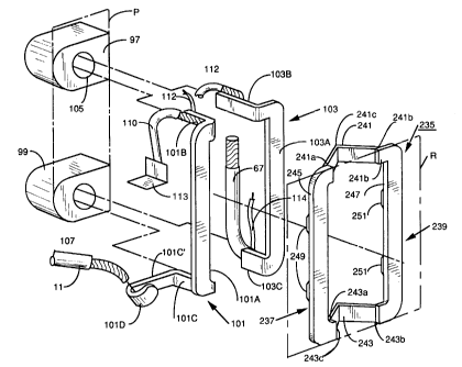
These conductors 101 and 103 are flat bus bars
formed from sheet material. As best seen in Figure 4, the
neutral bus bar 101 has a flat center section 101a extend-
ing parallel to a common plane P containing the end faces
5 of the toroidal coils 97 and 99. A flat leg section 101b
extends generally laterally from the upper end of the
center section of 101a and is bent substantially at a right
angle to the flat center section. A second leg section
101c extends generally laterally from the lower end of the
10 center section 101a and is bent transversely to the flat
center section. A terminal portion lOlc' of the leg lOlc
is bent generally perpendicular to the leg 101c to extend
in a plane generally parallel to the plane of the flat
center section 101a. A crimp 101d is formed in the end of
the terminal portion 101c'. Preferably, this crimp 101d is
bent at an angle in the plane of the terminal portion 101c'
for a purpose to be discussed.
The line bus bar 103 also has a flat center
section 103a and a first leg section 103b extending gener
ally laterally from the upper end center section and bent
generally perpendicular to the plane of the center section
103a. A second leg section 103c extends laterally from and
is bent generally perpendicular to the lower end of the
flat center section 103a.
The upper legs 101b and 103b and the lower legs
101c and 103c extend from opposite sides of the respective
center sections 101a and 103a of the neutral bus bar 101
and the line bus bar 103 so that when the two bus bars are
placed side by side the flat upper leg sections 101b and
103b, and the flat lower leg sections 101c and 103c, are in
spaced, flat confronting relation. The upper leg sections
101b and 103b extend through the central aperture 105 of
the toroidal coil 97 while the leg sections 101c and 103c
extend through the central aperture 107 in the toroidal
coil 99.
__ 210~~18
11
The crimp 101d on the terminal portion 101c' of
the lower leg 101c on the neutral bus bar 101 secures this
bus bar to the neutral pigtail 11. The crimp 101d is bent
at an angle to the terminal portion 101c' of the lower leg
101c so that the pigtail is lead directly from the crimp to
the opening 111 in the housing 3. The upper leg 101b of
the neutral conductor 101 is connected by an insulated lead
110 to a tang 113 which is secured to the load neutral
terminal 7. This upper end of the neutral bus bar 101 is
also connected by the lead 112 to the printed circuit board
91.
The lower end of the line bus bar 103 is connected
by the flexible conductor 67 to the bimetal 61 and is also
connected by a lead 114 to the printed circuit board 91.
The upper end of the line bus bar 103 is connected through
an opening in the central panel 23 to the tang 69 leading
to the load terminal 5. The windings on the toroidal
sensing coils 97 and 99 form the secondaries of the sensing
transformers.
In an exemplary embodiment of the invention, the
neutral bus bar 101 and line bus bar 103 are formed from
copper sheet material having a thickness of 0.047 inches
(1.2 mm). The center sections are .135 inches (3.4 mm)
wide and the legs are .125 inches (3.175 mm) wide. With
these bus bars, the circuit breaker 1 has a rated current
of 50 amperes. With the prior art insulated wire used as
the neutral and line conductors for the sensing transform-
ers, the 0.220 inch (5.59 mm) diameter of the central
apertures 105 and 107 of the sensing coils limit the rated
current of the circuit breaker 1 to 30 amps using 10 gauge
twisted wire. Thus, the bus bars 101 and 103 allow the
rating of the ground fault circuit breaker to be increased
without major modification to the circuit breaker struc-
ture.
The neutral and line bus bars 101 and 103 are
electrically insulated from each other, and from surround-
ing components by a one piece insulating barrier 235. The
mo5~ts
12
insulating barrier 235 comprises a pair of confronting C-
shaped insulating members 237 and 239 in a common plane R
joined by linear sections 241 and 243. The C-shaped
members 237 and 239 conform to the shape of the center
portions 101a and 103a and the portions of the bent legs B
and C which are in the same plane as the center sections.
These C-shaped members 237 and 239 have edge extensions 245
and 247, respectively, which extend over the side edges of
the conductors 101 and 103. The linear sections 241 and
243 join the C-shaped members 237 and 239 in the plane of
the bottom edge extensions 245 and 247. These linear
sections 241 and 243 are hinged at their connections 241A
and 243A with the C-shaped member 237 and at hinge connec-
tions 241B and 243B at the connection with the C-shaped
member 239. The linear sections 241 and 243 are also
formed with score line 241C and 243C at their mid-points.
trippers 249 and 251 are molded into the edge extensions
245 and 247, respectively.
The insulating barrier 235 can be formed flat in
a vacuum forming process. The linear sections 241 and 243
are then folded at the hinge lines 241a-b, 243a-b and score
lines 241c and 243c to form projections 253 which extend
transverse to the common plane of the C-shaped members 237
and 239 as shown in Figure 5. This also brings the C
shaped members 237 and 239 close together to the same
spacing as the conductors 101 and 103. The projections 253
are then pressed between the facing depending legs 101B,
103B and 101C, 103C, respectively, with the C-shaped
members 237 and 239 fitting down over the center sections
101A and 103A. The grippers 249 and 251 snap under the
bottom surfaces of the conductors 101 and 103 to secure the
insulating barrier 235 in place. A suitable material for
the insulating barrier 235 is 0.010 inches or .25 thick
polycarbonate.
An alternate form of the insulating barrier 257 is
illustrated in Figure 6. In this embodiment, the insulat-
ing barrier 257 is formed with the projections 259 and 261.
._ 210~~18
13
These projections 259 and 261 space the confronting C-
shaped members 263 and 265 properly to snap over the
conductors 101 and 103, without folding, as in the previ-
ously described embodiment.
In operation, upon detection of a grounded load
conductor or a grounded load neutral conductor through the
toroids 97 or 99, the ground fault circuit 119 energizes a
trip solenoid 123. Energization of the trip solenoid 123
results in extension of the solenoid plunger 127. A flag
129 secured to the plunger extends through a slot 131 in
the center panel 25 and pushes the armature 71 to the right
as viewed in Figure 2 to trip the circuit breaker thereby
opening the separable contacts 29.
In order to allow for periodic verification of the
operation of the circuitry, a test circuit is provided
which includes the test switch 17, accessible from the
outside of the housing 3 as seen in Figure 1. More specif
ically, a test wire 121 is connected between the neutral
conductor 101 and the load conductor 103 by way of the test
switch 139 of the test switch 17, which closes contacts 135
and 137, and is routed through the toroid 97 (Fig. 3) to
induce a signal in the secondary winding T1 to simulate a
ground fault condition. Upon actuation of the test button
139, a ground condition is simulated, resulting in a trip
of the circuit breaker through energization of the trip
solenoid 123.
The lower end of the neutral 101 is welded to the
end of the pigtail 11 extending through an opening 111 in
the housing 3 for connection to a panel neutral. The upper
end of the neutral lead 1a1 is connected to the printed
circuit board by a lead 112 and to a tang 113 leading to
the load neutral terminal 7. The lower end of the line
lead 103 is connected to the flexible conductor 67 leading
from the bimetal 61 and by lead 114 to the printed circuit
board, while the upper end is connected through an opening
in the central panel 23 to the tang 69 leading to the load
CA 02105918 2000-OS-08
14
terminal 5. The windings T1 and T2 on the toroidal sensing
coils 97 and 99 form the secondaries of the transformers.
The schematic diagram of the circuit 119 of the
ground fault detector which is mounted on the printed
circuit board.91 is. illustrated in Figure 7. The circuitry
119 includes the sensing toroids 97 and 99 with secondary
windings T1 and T2, respectively. As previously discussed,
the line conductors 103 as well as the neutral conductor
101, are routed through the toroids 97 and 99. Additional-
1y, a test conductor 121 is routed through the upper toroid
97.
The toroid 97 is used for sensing ground faults.
During normal conditions, the magnetic fields generated by
the conductor 103 amd the neutral conductor 101 cancel and
therefore do not induce a voltage on the secondary winding
T1 of the thyroid 97. However, during a ground fault
condition, there will be a resultant magnetic field which
will induce a voltage in the secondary winding T1 which, in
turn, will energizE: a trip solenoid 123 by way of a ground
fault interrupter integrated circuit IC1, as discussed
below.
The toroi.d 99 is used in conjunction with the
toroid 97 fo:r sensing a grounded neutral condition. As
discussed in Linear Integrated Circuits 1989 by Raytheon
Corporation, Section 10 on pages 10-16 through 10-21,
a grounded nE~utral will close a magnetic path between the
toroids 97 and 99. The resultatant AC coupling closes a
feedback path around an operational amplifier in the IC1
causing the operational amplifier to oscillate. When the
peaks of the oscillation voltage exceed an CR trigger
comparator threshold within the IC1, the IC1 output will go
high. Circuitry for detecting a grounded neutral condition
is also disclosed in United States Reissue Patent No.
30,678.
'1'L1C secondary windings T1 and T2 of the toroids 97
and 99, respectively, are applied to a low power ground
fault interrupter integrated circuit IC1, such as a
Raytheon RV4:145 or a TRC-10020 by Technology Research
15
Corporation of Clearwater, Florida. More specifically, one
side of the secondary winding T1 is applied to pin 3 of the
integrated circuit IC1. The other side of the secondary
winding T1 is applied to pin 1 of the IC1 by way of the
resistor R1 and serially coupled capacitor C1. A resistor
R2 is connected between pins 1 and 8 of the integrated
circuit IC1. The resistors R1 and R2 determine an amplifi-
cation factor for an operational amplifier within the
integrated circuit IC1. Exemplary values for the resistors
R1 and R2 are 150 ohms and 1 megohm, respectively. The
capacitor C1 which may be, for example, 15 microfarads acts
as a coupling capacitor. A noise capacitor C2, for exam-
ple, 0.01 microfarads is connected between pins 1 and 2 of
the integrated circuit IC1.
One side of the secondary winding T2 is connected
to the secondary winding T1 that is connected to pin 3 of
the integrated circuit IC1. The other side of the second-
ary winding T2 is connected to a tuning capacitor C3, for
example, 1 microfarad. The other side of the tuning
capacitor C3 is connected to the resistor R2, pins 7 and 8
of the integrated circuit IC1 as well as to a noise capaci-
tor C4, for example, 0.01 microfarads. The other side of
the noise capacitor C4 is connected to pin 4 of the inte-
grated circuit IC1.
The winding of the trip solenoid 123 is connected
on one end to the line conductor 103 with the other end
connected to a full wave rectifier, generally indicated by
the reference numeral 125, and including the diodes D1, D2,
D3 and D4. The do output of the full wave rectifier 125
is connected across a silicon controlled rectifier SCR 1.
The gate terminal of the silicon controlled rectifier SCR
1 is connected to pin 5 of the integrated circuit IC1. A
noise capacitor C5, for example 6.8 microfarads is connect-
ed between the gate terminal of the silicon controlled
rectifier SCR 1 an pin 4 of the integrated circuit IC1 to
prevent spurious triggering of the silicon controlled
rectifier SCR 1.
A resistor R4, for example 30 kilohms, is con-
nected between full wave rectifier 132 and pin 6 of the
CA 02105918 2000-OS-08
16
integrated c:ircuiit IC1. This resistor limits the
current to the :shunt regulator within the integrated
circuit IC1. Surge protective devices, such as the
varistors RV:L and :RV2 are used to protect the circuit from
overvoltage.
In operai:ion, upon detection of a grounded load
conductor or a grounded load neutral conductor by the
toroids 97 or 99, a voltage is induced in the secondary
windings T1 <~nd T2. This voltage, in turn, is applied to
the integrated circuit IC1. During such conditions, pin 5
of the integrated circuit IC1 enables the gate terminal to
fire the silicon controlled rectifier SCR 1, which, in
turn, energi2;es thE; trip solenoid 123. Energization of the
trip solenoid 123 results in extension of the solenoid
plunger 127. A flag 129 secured to the plunger extends
through a slot 131. in the center panel 25 and pushes the
armature 71 t:o the right as viewed in Figure 2 to trip the
circuit breal~:er thereby opening the separable contacts 29.
In order to allow for periodic verification of the
operation of the circuitry, a test circuit 132 is provided
which includes thc~ test switch 17, accessible from the
outside of the hour>ing 3 as seen in Figure 1. More specif
ically, the test wire 121 is connected between the load
neutral conductor 101 and the load conductor 103 by way of
the test switch 17, and a resistor R3, for example 15
kilohms, and is routed through the toroid 97 (Fig. 3) to
induce a signal in the secondary winding T1 to simulate a
ground fault condii~ion. Upon actuation of the test button
17, a ground condition is simulated, resulting in a trip of
the circuit breaker through energization of the trip
solenoid 123.
Referring to Figures 3, 8 and 9, the test switch
17 includes a. fixed contact 135, a movable contact 137 and
a test button 139. The fixed contact 135 and the movable
contact 137 each comprise an electrically conductive
metallic strip, suc:h as a copper strip. The metallic strip
of the fixed contact 135 has a base section 141 which is
secured alone a side edge 143 to the printed circuit board
by a latera:Lly e:~tending projection 145 which extends
._
17
through the printed circuit board and is soldered in place
on the back of the printed circuit board. The solder joint
146 also electrically connects the fixed contact 135 to a
lead trace 147 in the test circuit of the printed circuit
board. The fixed contact has a terminal section 148
cantilevered laterally from the end of the base section
141. The movable contact 137 similarly has a base section
149 and a terminal section 151 and is similarly secured
along the side edge of the base section 149 to the printed
circuit board. The fixed and movable contacts 135 and 137
are nested in spaced relation with the base portions
substantially parallel. The terminal section 151 of the
movable contact 137 extends at substantially a right angle
to the base section 149, while the angle between the base
section and terminal section of the fixed contact is
slightly greater than a right angles so that the terminal
section 148 angles slightly toward the terminal section 151
of the movable contact 137.
The test button 139 includes an enlarged head
portion 153 which is received in a recess 155 in an upward
ly extending bass 157 molded into the housing 3. A stem
159 on the underside of the head 153 extends through a
guide opening 161 in the housing 3 and terminates and an
enlarged terminal portion 163. The terminal section 151 of
the movable contact 137, which is resiliently deformable,
being made of copper, bears against the terminal portion
163 and biases the button to the full upward or unactuated
position shown in Figure 3. The button 139 is retained by
the terminal portion 163 which bears against the portion of
the housing 3 forming the guide opening 161. With the test
switch 17 in its unactuated position, the test circuit 119
is open circuited. When the ground fault detector is to be
tested, the test button 139 is depressed thereby resilient-
ly deforming the movable contact 137 to bring it into
electrical contact with the fixed contact 135 to complete
the test circuit as shown in Figure 6.
._ ~10~~18
18
While specific embodiments of the invention have
been described in detail, it will be appreciated by those
skilled in the art that various modifications and alterna-
tives to those details could be developed in light of the
overall teachings of the disclosure. Accordingly, the
particular arrangements disclosed are meant to be illustra-
tive only and not limiting as to the scope of the invention
which is to be given the full breadth of the appended
claims and any and all equivalents thereof.