Note: Descriptions are shown in the official language in which they were submitted.
2~0~325
TITLE OF THE INVENTION
GATE POWER SUPPLY CIRCUIT
BACKGROUND OF THE INVENTION
Field of the Invention
This invention relates to a gate power supply circuit,
and more particularly to a gate power supply circuit that
supplies gate power to the gate drive circuit for a self-
turn-off device from a main circuit, utilizing the switching
action of a self-turn-off device etc.
Description of the Related Art
By employing self-turn-off devices in a power converter
such as an inverter, the benefits are obtained of better
suppression of source side and load side harmonics than
hitherto, improvement of the power source power factor, and
device miniaturization, etc. Hitherto, it was impossible to
obtain self-turn-off devices suited for high voltage and
larger current use. Recently however, it has become
possible to manufacture self-turn-off devi1es typified by
~TOs suited for high voltage and large current use.
Application of self-turn-off devices to the high power field
-- 1 --
2~06325
has therefore become common.
When applying self-turn-off devices such as GTOs to
high voltage applications, the problem of the drive power
source of the gate drive circuit of the self turn-off device
cannot be neglected. This problem is particularly severe in
the case of GTOs constituting switching elements mainly
employed in the high power field. The reason for this is
that a GTO is a current-controlled device, yet the degree of
current amplification on turn-off is small, so, on turn-off,
a very large current the amplitude of which is about one
third through one fifth of that of the main circuit current,
must be supplied to the gate of the GTO. Furthermore, even
when the GTO is ON, current to the gate must be con~inued in
order to reduce conduction loss. The power consumption of
the gate drive circuit of a GTO is therefore at least 100 W
per GTO, although this does vary depending on the type of
GTO.
Since the gate drive circuit of a GTO is directly
connected to the cathode and gate of the GTO that is being
driven, it is electrically at the same potential as the
cathode of ~he GTO that is being driven. When GTOs are
connected in series, the gate drive circuit of each GTO is
at a respectively different potential, so the power sources
of the respective gate drive circuits must be at
respectively different potentials. This means that the
power sources of the gate drive circuits of the GTOs must be
2~32~
mutually insulated for each respective GTO.
An example of a conventionally used GTO gate drive
circuit is shown in Fig. 9. Fig. 9 shows a single GTO oE a
plurality of GTOs constituting a power converter and the
associated snubber circuit and gate drive circuit.
In Fig. 9, a CTO 1 is ~he main switching device. A
snubber diode 2 and a snubber capacit~r 3 constitute a
snubber circuit for suppressin~ the rate of voltage rise
when GTO 1 is turned OFF, and suppress GTO loss on turn-off.
A resistor 4 dissipates the energy stored in snubber
capacitor 3. A diode 5 is a free-wheeling diode that
provides a current path for the main circuit current in
regeneration mode. A resistor 6 is a DC balance resistor
tha~ performs the action of balancing the DC voltages
apportioned to each GTO when a large number of GTOs are
connected in series, so that they are not affected by the
slight variations of the characteristics of each GTO.
The gate of GTO 1 is driven by a ~ate drive circuit 7.
The ON~OFF signal of the gate is ~ransmitted as an optical
signal by an optical fiber 8 and is converted to an
electrical signal by a photoreceptor module, ~ot shown, in
gate drive circuit 7. Since an optical signal is employed,
the ON/OFF gate signals are automatically insulated for each
GTO 1. Regarding the power source of gate drive circuit 7,
this can be obtained by using a rectifier 9 to produce DC
power by rectifying the high frequency (such as 20 kHz) AC
21~325
power supplied from a high frequency AC power source 11
through an isolating transformer 10. High frequency AC
power source 11 is located in a low potential zone and is
supplied in common to each GTO; the difference in potential
between GTOs 1 is insulated by means of isolating
transformer 10 corresponding to each respective GTO 1.
However, there are considerable problems in applying
the prior art to power converters in which a large number of
GTOs are connected in series and the DC bus voltage exceeds
a few tens o~ kV. This is because a large number of
isolating transformers capable of withstanding a high
voltage of a few tens of kV to be isolated across their
poles and capable of insulating ~he high voltage are
required in order to achieve delivery of high frequency AC
power through isolating transformers 10 from the low
potential zone. Not only do such isolating transformers
require a large amount of space, but in addition they are
enormously expensive. There were therefore problems on
grounds of space and cost in applying the prior art to high
voltage application, such as power converters, in which a
large number of GTOs were connected in series.
SUMMARY OF THE INVENTION
Accordingly, one object of this inven~ion is to provide
a gate power supply circuit which can dispense with an
2la~3~ .
isolating transformer and enables miniaturization and cost
reduction of a power converter constructed using self-turn-
off devices.
These an~ other objects of this invention can be
achieved by providing a gate power supply circuit including
a switching device and a gate drive circuit connected to the
switching device for generating a gate signal to be supplied
to a gate of the switching device. The gate power supply
circuit further includes a series circuit of a snubber
capacitor and a snubber diode connected in parallel with the
switching device, and an inductor, a first terminal of which
is connected to a connection point of the switching device
and the s~ubber diode. The gate power supply circuit also
includes a series circuit of power disposing circuit and a
first diode, connected between a series connection point of
the snubber capacitor and ~he snubber diode and a second
terminal of the inductor. The ~ate power supply circuit
further includes a series circuit of a power supplying
capacitor and a second diode, connected in parallel with the
inductor. The gate drive circuit is connected to the power
supplying capacitor to receive energy stored in the power
supplying capacitor as power source for the gate drive
circuit.
According to one aspect of this invention, there is
2106325
provided a gate power supply circuit including a plurality
of valve units, an inductor having a first terminal and a
second terminal and a power disposing circuit. A first
terminal of the power disposing circuit is connected to the
second terminal of the inductor. Each of the valve units
includes a switching device, a gate drive circuit co~nected
to the switching device for generating a gate signal to be
supplied to a gate of the switching device, a series circuit
of a snubber capacitor and a snubber diode connected in
parallel with the switching device, a first diode, a first
terminal of which being connected to a series connection
point of the snubber capacitor and the snubber diode, and a
series circuit of a power supplying capacitor and a second
diode. A first terminal of the power supplying capacitor is
connected to a connection point of the switching device and
the snubber diode, and a second terminal of the power
supplying capacitor is connected to a first terminal of the
second diode. The gate drive circuit is connected to the
power supplying capacitor to receive energy stored in the
power supplying capacitor as power source for the gate drive
circuit. A plurality of the valv~ units and the inductor
are connected in series, such that a plurality of the
switching devices are connected in series, and the inductor
is connected in series with the series connected switching
devices such that the first terminal of the inductor is
connected to the connection point of the switching device
3 2 5
and the snubber diode of the valve unit in a last stage. A
second terminal of the first diode of the valve unit in a
stage except the last stage is connected to the first
. _
terminal of the first diode of the valve unit in a next
stage, and a second terminal of the first diode of the valve
unit in the last stage is connected to a second terminal of
the power disposing circuit. A second terminal of the
second diode of the valve unit in the stage except the last
stage is connected to the first terminal of the second diode
of the valve unit in the next sta~e, and a second terminal
of the second diode of the valve unit in the last stage is
connected to a second terminal of the inductor.
Consequently, the feature of this invention is to
provide a gate power supply circuit so arranged that power
supplied to the gate drive circuit is obtained from the main
circuit by utilizing to ON/OFF action of the self-turn-off
device, dispensing with an isolating transformer.
BRIEF DESCRIPTION OF THE DRAWINGS
A more complete appreciation of the invention and many
of the attendant advantages thereof will be readily obtained
as the same becomes better understood by reference to the
following detailed description when oonsidered in connection
with the accompanying drawings, wherein:
-' 210~325
Fig. 1 is a layout diagram showing a gate pow~r supply
circuit according to a first embodiment of this invention;
F~g. 2 is an operating waveform diagram given in
explanation of the operation of the gate power supply
circuit of Fig. 1;
Fig. 3 is a layout diagram showing a gate power supply
circuit according to a second embodiment of this invention;
Fig. 4 is an operating waveform diagram ~iven in
explanation of the operation of the gate power supply
circuit shown in Fig. 3;
Fig. 5 is a layout diagram showing a gate power supply
circuit according to a third embodiment this invention;
Fig. 6 is a layout diagram showing a gate power supply
circuit according to a four.th embodiment of this invention;
Fig. 7 is a layout diagram showing a gate power supply
circuit according to a fifth embodiment of this invention;
Fig. 8 is a layout diagram showing a gate power supply
circuit according to a sixth embodiment of this invention;
and
-- 8 --
. .~
210632~
Fig. 9 is a layout diagram showing a prior art gate
power supply circuit.
DETAILED DESCRIPTION OF T~E PREFERRED EMBODIMENTS
Referring now to the drawings, wherein like reference
numerals designate identical or corresponding parts
throughout the several views, the embodiments of this
invention will be described below.
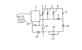
Fig. 1 is a layout diagram showing a gate power supply
circuit according to a first embodiment of this invention.
In this Figure, 1 is a self-turn-off device (hereinbelow
referred to as GTO 1) of the main circuit. A snubber
circuit consisting of the series circuit of a snubber diode
2 and snubber capacitor 3, fre~-wheeling diode S and DC
balance resistor 6 are connected in parallel with GTO 1.
One terminal of an inductor 12 is connected to the cathode
side of GTO 1, while a series circuit consisting of a first
diode 15 and a first capacitor 16 is connected between ~he
other terminal of inductor 12 and the series connection
point of snubber diode 2 and snubber capacitor 3, and a
resistor 17 is connected in parallel with capacitor 16.
Furthermore, a series circuit consisting of a power
supplying capacitor, such as a second capacitor 13, and a
second diode 14 is connected in parallel with inductor 12,
2~0~32~
so that the energy stored in second capacitor 13 is fed to
gate drive circuit 7.
The operation of this invention constructed as above
will now be described with reference to Fig. 2. In Fig. 2,
VAK is a voltage between an anode and a cathode of GTO 1,
VC13 is a voltage of second capacitor 13, ID14 is a current
flowing through second diode 14 and VL12 is a voltage of
inductor 12.
Whilst GTO 1 is OFF, snubber capacitor 3 is charged
through snubber diode 2 and inductor 12 practically up to
the DC apportioned voltage VAK of GTO 1.
At time point A in Fig. 2, GTO 1 is turned ON and
voltage VAK of GTO 1 drops. Simultaneously, first diode 15
conducts,.and the charge of snubber capacitor 3 is
discharged by the loop: GTO 1 - inductor 12 ~ first
capacitor 16 ~ first diode 15. Since the voltage VAK of GTO
1 rapidly approaches zero, voltage VL12 of inductor 12
becomes diractly that of snubber capacitor 3. Dischar~e of
snubber capacitor 3 terminates at time point B. After ti~e
point B, the current of inductor 12 flows in the first loop:
inductor 12 - first capacitor 16 - first diode 15 ~ snubber
diode 2 - inductor 12, and in the second loop: inductor 12
second diode 14 ~ second capacitor 13 - inductor 12.
Thereby, second capacitor 13 is charged, and the volta~e
VC13 of second capacitor 13 rises. At the time point C
where the current in inductor 12 that flows due to the
-- ~0 --
21~632~
snubber energy becomes zero, the snubber energy that has
been transferred to inductor 12 has all completed its
transfer to first capacitor 16 and second capacitor 13. The
_
energy stored in first capacitor 16 is dissipated by
resistor 17 and the energy stored in second capacitor 13 is
supplied to gate drive circuit 7.
If first capacitor 16 of sufficiently large capacity is
employed, the voltage of first capacitor 16 always maintains
a practically constant voltage level. Since the charged
voltage of second capacitor 13 is equal to the volta0e of
first capacitor 16, if the value of first capacitor 16 is
made sufficiently large, every time GTO 1 is turned ON, the
voltage of second capacitor 13 will be charged up to a fixed
voltage equal to the voltage of first capacitor 16. In this
case, the voltage of first capacitor 16 is determined by the
value of resistor 17 and the input power to first capacitor
16 that is determined by the switching frequency of GTO 1
and the energy stored in snubber capacitor 3 during the
period while GTO 1 is OFF.
In this embodiment, the energy stored in the power
supplying capacitor, such as second capacitor 13, is
supplied to gate drive circuit ~, so that an isolating
transformer of high withstand voltage that is necessary in
the prior art shown in Fig. 9 can ~e omitted.
Fig. 3 is a layout diagram showing a gate power supply
circuit according to a second embodiment of this invention.
-- 11 --
21~325
.
In ~his second e~bodiment, a single switching valve is
cons~ituted by connecting in series four GTOs la, lb, lc and
ld that are driven by the same ~ate si~nal. It is to be
noted that, in this specification, suffixs a, b, c and d are
attached to reference numerals indicating compone~ts in
valve units a, b, c and d constituting a single switching
valve, respectively. In the case of high volta~e
applications wherein a lar~e number of switching devices are
connected in series, the arm of a power converter is
constituted by further connecting a large number of the
switching valves thereby obtained in series. In the second
embodiment, the rate of current rise of the GTO is
suppressed by a single anode inductor 12 provided in a
single switching valve. Even in the case of the gate power
supply circuit of this invention, a single anode inductor 12
is used in common with four gate supply circuits.
What is important in the operation of the second
embodiment is series-connected second diodes 14a, 14b, 14c
and 14d and first diodes 15a, 15b, 15c and 15d. Whilst GTOs
la, lb, lc and ld are OFF, these diodes are reverse-biased,
and so do not conduct, with the result that the GTOs la to
ld are respectively isolated. When GTOs la to ld are turned
ON, these diodes conduct during the period in which the
current of inductor 12 flows in the respective diodes, and
snubber capacitors 3a, 3b, 3c and 3d are equivalently
connected in parallel; also, second capacitors 13a, 13b,
2106325
13c and 13d have a configuration in which they are
equivalently connected in parallel. The operation of this
second embodiment will now be described in detail with
reference to Fig. 4.
At time point A in Fig. 4, GTOs la to ld turn ON, and
the voltages VAK of GTOs la to ld drop. Simultaneously,
first diodes 15a to 15d conduct. The charge of snubber
capacitor 3d starts to be discharged by the loop: snubber
capacitor 3d - GTO ld - inductor 12 -- first capacitor 16 -
first diode 15d ~ snubber capacitor 3d. Also, the charge of
snubber capacitor 3c is discharged by the loop: snubber
capacitor 3c - GTO lc - GTO ld -~ inductor 12 ~ first
capacitor 16 - first diode 15d ~ first diode 15c - first
snubber capacitor 3c. The charge of snubber capacitor 3b is
discharged by the loop: snubber capacitor 3b - GTO lb - GTO
lc GTO ld - inductor 12 -- first capacitor 16 - first diode
15d first diode 15c - first diode 15b - snubber capacitor
3b. In the same way, the charge of snubber capacitor 3a is
discharged by the loop: snubber capacitor 3a ~ GTO la - GTO
lb - GTO lc GTO ld inductor 12 - first capacitor 16 -
first diode 15d - first diode 15c - first diode 15b first
diode 15a - snubber capacitor 3a. Since voltages VA~ of
GTOs la to ld rapidly approach zero, voltage'VL12 of
inductor 12 bebomes the same as the voltage of snubber
capacitors 3a to 3d which have becoms equivalently connected
in parallel. Discharge of snubber capacitor 3a to 3d ceases
- 13 -
2106325
at time point B. After time point B, the current of
inductor 12 flows in the loops: inductor 12 - first
capacitor 16 ~ first diode 15d - snubber diode 2d - inductor
12. The current of inductor 12 flows also in the loop d:
inductor 12 - second diode 14d ~ second capacitor 13d -
inductor 12; furthermore, it flows in the loop c: induc~or
12 ~ second diode 14d second diode 14c - second capacitor
13c ~ GTO ld - inductor 12, in the loop b: inductor 12 ~
second diode 14d - second diode 14c - second diode 14b -
second capacitor 13b ~ GTO lc ~ GTO ld - inductor 12, and in
the loop a: inductor 12 ~ second diode 14d - second diode
14c - second diode 14b - second disode 14a - second
capacitor 13a ~ GTO lb - GTO lc - GTO ld ~ inductor 12. In
this way, in second diode 14a, there flows the current that
charges second capacitor 13a and, in second diode 14b, in
addition to the current that charges second capacitor 13b,
there flows the current that charges second capacitor 13a.
In second diode 14c, there flows the currents that charge
second capacitors 13c, 13b and 13a, respectively, and in
second diode 14d, there flows the currents that charga
second capacitors 13d, 13c, 13b and 13a, respectively.
Consequently, as shown in Fi~. 4, as one goes down through
the four series-connected second diodes 14a to 14d, it will
be found that these are passing progressively more currents
ID14a to ID14d. Second capacitors 13a to 13d are thereby
charged, and the respective volta~es VC13a, VC13b, VC13c and
- 14 -
~10~325
VC13d of second capacitors 13a to 13d rise. At the time
point C when the current of inductor 12 that flows due to
the snubber energy has become zero, all of the energy of
inductor 12 has completed its transfer to second capacitors
13a to 13d. The energy stored in first capacitor 16 is
dissipated by resistor 17, and the energies stored in second
capacitors 13a to 13d are respectively fed to gate drive
circuits 7a to 7d.
The number of GTOs in Fig. 3 is four, but there is no
res~riction to four, and the arrangement can ~e put into
practice with any number of GTOs connected in series.
In the embodiments so far described, the energy stored
in first capacitor 16 was dissipated by resistor 17. This
layout involves only a small number of components, but in
particular in high voltage applications, results in
considerable losses, lowering efficiency as a power
converter.
In order to reduce this drop in efficiency, the third
embodiment of this invention, shown in Fig. 5 may be
employed. In this embodiment, instead of resistor 17, use
is made of a chopper or DC/DC converter or the like, so that
the energy stored in first capacitor 16 can be regenerated.
In the third embodiment of this inventi~n, shown in
Fig. 5, instead of resistor 1~ connected in parallel with
first capacitor 16 in the second embodiment of this
invention shown in Fig. 3, there is provided a snubber
- 15 -
2~63~5
energy regeneration circuit 18 constituted by a chopper or
DC/DC converter or the like. The construction of the
snubber energy regeneration circuit 18 is well known to
those skilled it the art, so that the detailed descrip~ion
thereof may by ~mitted. The rest of the layout is the same
as Fig. 3. The opera~ion of this third embodiment therefore
differs only in that the energy stored in first capacitor 16
is regenerated at the power source side of load side by
snubber energy regenerating circuits 18. With such a
layout, the voltage of first capa_itor 16 i5 controlled by
the action of snubber energy regenerating circuit 18 such as
to be a fixed voltage.
In this invention, the energy stored in the snubber
capacitor of the switching de~ice in the OFF period of the
switching device provides the source of the drive power of
the gate drive circuit. Therefore, after the power source
of the power converter is connected, gate drive power will
not be supplied until the switching device commences its
switchin~ action. Where there are many switching devices,
not much power is required to turn them ON. In particular,
in the case of an IGBT or MCT, which is an MOS gate ~ype
switching device, practically no gate power is required for
turn ON. Initial turn ON i.e. first turn ON after power
source connection, can therefore be arranged to be performed
by extracting only a slight gate power from an optical
signal using for example a photovoltaic elemen~, it bein~
- 16 -
2~06325
arranged for the gate power to be suppli~d subsequently from
the gate power supply circuit of this invention.
However, this method is difficult to apply in the case
of switching devices such as GTOs. This is because most
GTOs need a certain amount of gate power to provide negative
bias to the gate even when the GTO is OFF.
Fig. 6 is a layout diagram showing a gate power supply
circuit accordin~ to a fourth embodiment of this invention
adapted for such cases. In this embodiment, instead of DC
balance resistor 6 in the embodiment of Fig. 1, a voltage
dividing-circuit consisting of volta~e dividing resistors 6a
and 6b connected in series is connected in parallel with GTO
1, so that second capacitor 13 is charged during the OFF
period of GTO 1. In this way, gate power is supplied
through the voltage-dividing circuit before GTO 1 begins
switching. In Fig. 6, voltage-dividing resistors 6a and 6b
also perform the role of balance resistor of GTO 1. Of
course, there would be no problem in providing a balance
resistor apart from voltage-dividing resitors 6a and 6b,
but, from the point of view of space and cost, it is
advantageous to combine these functions. In Fig. 6, the
voltage obtained by the voltage division of voltag~ dividing-
resistors 6a and 6b is supplied to gate drive circuit I
be~ore GTO 1 starts switching. ~owever, if the dissipation
current of gate drive circuit 7 is considered, voltage
division may not necessarily be essential, and it may be
2~632~
possible to achieve the object simply by passing current
through the resistor.
Fig. 7 is a layout diagram showing a gate power supply
- _ .
circuit according to a fifth embodiment of this invention
for use in such a case.
The current that flows through resistor 6c before GTO 1
starts switching constitutes the power source of gate drive
circuit 7. In this case, a suitable voltage stabilizing
means must be incorporated on the side of the yate drive
circuit 7, but this can easily be implemented and need not
therefore be shown as a practical example.
If gate drive circuit 7 incorporates a voltage
stabilizing means, some fluctuation of the source voltage of
gate drive circuit 7 can be permitted. In this case, first
capacitor 16 of the embodiment of Fig. 1 is not necessarily
essential. The reason for this is that first capacitor 16
serves for receiving the energy stored in inductor 12; once
it has been received in first capacitor 16, it is dissipated
by resistor 17 or it should be regenerated by a DC/DC
converter or the like; there is therefore no problem in
allowing the energy to be directly dissipated by resistor 17
without passing through first capacitor 16.
Fig. 8 is a layout diagram showing a gate power supply
circuit according to a sixth embodiment of this invention
based on this concept. Thè embodiment of Fig. 8 is
characterized in that, compared with the embodiment of Fig.
- 18 -
21~6325
1, first capacitor 16 is not provided and the energy is
directly dissipated by resistor 1~. As already mentioned,
the larger first capacitor 16 i~ made, the more stable will
_,
its voltage be, so if on the other hand first capacitor 16
is absent, there will be considerable fluctuation of the
source voltage of gate drive circllit 7. However, this can
be allowed, due to the provision of voltage stabilizing
means within gate drive circuit 7.
The sixth embodiment is particularly beneficial where,
in the case of a low-snubber GTO with small capacity of
snubber capacitor 3, there is no energy worth returning for
regeneration, so first capacitor 16 is omitted and resistor
17 can be provided.
It should be noted that, although in the above
explanation, examples using GTOs as switching devices have
been described, this invention in not restricted to GTOs as
switching devices and could be employed with other self-turn-
off devices.
Furthermore, although in the above description the
switching device is taken as bein~ a GTO, so ~ is its gate
drive circuit, transistors or the like could also be
employed as switching devices. The gate drive circuit
therefore includes, the circuits to which this invention
could be applied, for example, fault detection circuits with
switching devices attached, or control and protection
circuits etc. for high potential units. In this invention,
- 19 -
210632~
these are designated by the general term "~ate drive circuit
or the like".
Yet further, although this invention is entitled "Gate
power supply circuit", as mentioned above, this invention
can also be applied to the case where transistors or the
like are employed as switching de~ices, so the term "gate
power supply circuit" is intended to include circuitry
whereby switchin0 devices such as transistors are
controlled.
As described above, with the ~ate power supply circuit
according to this invention, energy is obtained from the
main circuit side utilizing the switching action of
switching devices located in the main circuit, so the energy
stored in,the snubber capacitor during the off period of the
switching device is transferred to a power supplying
capacitor, such as a second capacitor, through an inductor
during the ON period of the switching device, thereby
enabling the energy stored in this second capacitor to be
utilized; the large number of isolating transformers of hi~h
withstand voltage that were necessary in the prior art are
thereby made unnecessary, enabling miniaturization and cost
reduction of a power converter constructed using self-turn-
off devices.
Obviously, numerous modifications and variations of the
present invention are possible in light of the above
- 20 -
2~ 0632~i
teachings. It is therefore to be understood that within the
scope of the appended claims, the invention may be practiced
otherwise than as specifically described herein.