Note: Descriptions are shown in the official language in which they were submitted.
21~?al~~
1
COMPUTER SYSTEM
BACKGROUND OF THE INVENTION
The present invention relates to a computer system,
and more particularly to a game computer system dealing with
both sound and image data.
Traditionally, in a computer system, sound is produced
from waveform data, which is generated by a computer program
based process; however, the quality of the sound has been low.
For that reason, sound data (analog signals) now are converted
into digital signals so that the sound waves may be synthesized
by an arithmetic operation.
In general, a game computer system uses a programmable
sound generator (PSG), which is small in size and capacity. In
the PSG, wave data supplied by a CPU are modulated in amplitude
or frequency in order to generate a sound wave. The PSG may
generate simple waves to intentionally produce noise. According
to the PSG, it is easy to control the output sound; however, it
is difficult to generate a variety of sounds.
In order to realize A/D conversion, a pulse code
modulation (PCM) method is used, by which an analog signal is
sampled at predetermined intervals, the sampled data are
quantized, and then, are transformed into binary data.
In another way, a difference PCM (DPCM) method, the
difference of the next two sampled data is quantized so that the
amount of output data to be transmitted i~ reduced. Further,
21~~'~'..~3.~
2
according to an adaptive difference PCM (ADPCM) method, the
quantizing process is performed at a short pitch when the next
two sampled data have a great difference, and on the other hand,
the process is performed at a long pitch when they have a small
difference. As a result, the output data may be mare
compressed.
The PCM and ADPCM data are compatible with each other
by compression and extension processing, the processing being
performed based on two kinds of conversion between scale value
and scale level, and among the ADPCM data, the changing amount
and changing level of the data.
In a game computer, ADPCM sound data stored in an
extra recording device are read by a CPU, and the data are
extended by an ADPCM decoder in accordance with scale value and
scale level to reproduce the original sound. The ADPCM decoder
contains a synchronizing signal generating circuit, which
generates a transmission rate, according to which the PCM data
are reproduced, by using a crystal resonator.
Recently, a game computer has not only sound sources
such as PSG and ADPCM controlled by the CPU, but also an
external audio device to realize high quality sound
reproduction. For example, in a game computer using a CD
(compact disk) as a recording medium, a CD player is directly
used as the PCM sound source.
In such a game computer system, it is desirable to
reproduce sound data in synchronization with each other to
~~~r~J~~
3
display image data. In a conventional system, the sound data
are reproduced in synchronization with their own synchronizing
signal generated in the ADPCM decoder, and the image data are
displayed in synchronization with vertical synchronizing
signals.
The CPU controls the outputs of the sound and image
data to be synchronized in accordance with the sound
synchronizing signal and vertical synchronizing signal. For
example, sound is reproduced in synchronization with an image
for each data set, that is, the image starts to be displayed
when the first data of the sound data set start being
reproduced. However, a time gap of outputs between the sound
and image data grows gradually with progression to the end of
the sound data set.
The CPU resets the ADPCM decoder to initialize the
scale level and PCM value. If the ADPCM data are not
transmitted accidentally or some tables occur in the
transmission, the scale level and PCM value may go out of order.
As a result, it becomes difficult to reproduce the sound
normally, unless the ADPCM data are reset to start reproducing
again. Even if the ADPCM data are reset, sound data may not be
reproduced in the middle, that is, the sound data must be
reproduced again from the start.
As another way, the ADPCM data are checked whether
they are transmitted normally, and when some tables occur in the
transmission, operation for reading ADPCM data is repeated until
CA 02107314 2000-10-13
4
normal data may be read. According to this processing, which is
called a "retry function," however, it takes long time to
restore to the normal condition.
Generally, image data occupy an area larger than that
of sound data in a memory. A variety of sound sources are used
in order to realize high quality sound reproduction with a small
amount of data. When a CD is employed as a sound storage
medium, the PSG, ADPCM or PCM decoder is used as a sound source.
The PSG decoder reproduces waveform sound, effect sound and the
like. The ADPCM decoder reproduces complicated natural sound,
human voice and the like. The PCM decoder reproduces sound that
is not necessary to be controlled in timing. According to the
ADPCM decoder, it is difficult to realize high quality sound
reproduction.
In the ADPCM decoder, ADPCM data are calculated by
omitting the figures after the decimal point in order to
reproduce the original sound. This omission causes an error in
the scale level and PCM value, which are used in the reproducing
process, and therefore, the original sound may not be reproduced
normally. The reproducing error is accumulated when a large
amount of ADPCM data are treated.
In the game computer system, it is required to change
the sampling frequency (reproducing rate) as needed.
SUMMARY OF THE INVENTION
Accordingly, it is an aspect of the present invention
CA 02107314 2000-10-13
to provide a computer system in which sound and image data may
be supplied in exact synchronization with each other.
In another aspect, the present invention provides a
computer system in which sound data may be well reproduced from
5 the middle.
In yet another aspect, the present invention provides
a computer system by which high quality sound reproduction may
be realized.
In a further aspect, the present invention provides a
computer system in which a reproducing rate (sampling
frequency) of ADPCM data may be changed easily.
According to a first feature of the present invention,
sound data are transmitted to an ADPCM decoder in
synchronization with a horizontal synchronizing signal,
according to which image data are transmitted.
According to a second feature of the present
invention, ADPCM (Adaptive Difference Pulse Code Modulation)
sound data are provided with control data which are not used in
normal condition. The control data are calculated in advance,
and used for calculating a proper decoding coefficient of an
ADPCM decoder. The ADPCM decoder uses the proper decoding
coefficient to reproduce the sound from the middle after
interruption.
According to a third feature of the present invention,
an ADPCM decoder reproduces original sound from ADPCM sound data
by arithmetic operation. The arithmetic operation is carried
2~.~J~131~
6
out using a rounding function.
According to a fourth feature of the present
invention, an ADPCM decoder holds the previous ADPCM data until
the following normal ADPCM data are transmitted thereto.
According to a fifth feature of the present invention,
a controller synchronizes the operations of ADPCM generator and
ADPCM decoder with each other. The same data are set in
registers contained in the ADPCM generator and ADPCM decoder to
specify a predetermined sampling frequency.
BRIEF DESCRIPTION OF THE DRAWINGS
Fig. 1 is a block diagram showing a computer system
according to the invention.
Fig. 2 is a timing chart showing a relation between
horizontal and vertical synchronizing signals.
Fig. 3 is a block diagram illustrating a sound data
output unit used in the computer system shown in Fig. 2.
Fig. 4 is an explanatory diagram showing a storage
configuration of ADPCM data in the memory, according to the
invention.
Fig. 5 is a table showing a relation among sampling
frequencies, adding amount in data transmission and adding
amount in a linear interpolation, according to the invention.
Fig. 6 is an explanatory diagram showing linear
interpolation in a 7. $7kHz sampling frequency mode, according to
the invention.
.~ ~ rl r~ .~
Fig. 7 is a flow chart showing a compressing process
for the ADPCM data, according to the invention.
Fig. 8 is a flow chart showing an extending process
for reproducing PCM data, according to the invention.
Fig. 9 is a table showing a relation among the ADPCM
data, variation values and level changing values, according to
the invention.
Fig. 10 is a table showing a relation between scale
levels and scale values, according to the invention.
Fig. 11 is a diagram showing the contents of an
operation register according to the invention.
Fig. 12 is a table showing the contents of a volume
control register according to the invention.
Fig. 13 is a timing chart showing operation of the
sound data output unit according to the invention.
Fig. 14 is a diagram showing the contents of ADPCM
decoder control registers according to the invention.
Fig. 15 is a timing chart showing operation of the
sound data output unit according to the invention.
Fig. 16 is a timing chart showing operation for
transmitting and reproducing sound data, according to the
invention.
Fig. 17 is a diagram showing the contents of a PSG
operation register according to the invention.
Fig. 18 is a diagram showing the contents of a volume
control register for the PCM data, according to the invention.
t) ~, ~~
Fig. 19 is a table showing interrelationships among
register values, amplifier and attenuation steps, and adjusting
speed, according to the invention.
Fig. 20 is an explanatory diagram showing arithmetic
operation for calculating a PCM value, according to the
invention.
Fig. 21 is a timing chart showing operation for
transmitting and reproducing sound data, according to the
invention.
Fig. 22 is a table showing level holding periods for
each sampling frequency, according to the invention.
Fig. 23 is a block diagram illustrating a control unit
used in the computer system shown in Fig. 2.
Fig. 24 is a block diagram illustrating the control
unit With other devices, according to the invention.
Fig. 25 is an explanatory diagram showing a storage
configuration of the ADPCM data in the memory, according to the
invention.
Fig. 26 is an explanatory diagram showing operation
for transmitting and reproducing the ADPCM data, according to
the invention.
Fig. 27 is a graph showing amplitudes of the sound
data, according to the invention.
Fig. 28 is a diagram showing registers used for
processing the sound data, according to the invention.
2.~~'~~1~~
9
DETAILED DESCRIPTION OF THE INVENTION
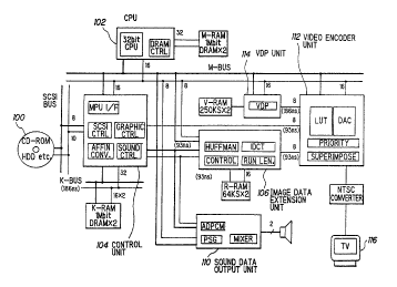
Fig. 1 shows a computer system, which includes a game-
software recording medium 100 such as a CD-ROM, a CPU 102 of the
32-bit type, a control unit 104 for mainly controlling
transmission of sound data and interfacing most devices to each
other, an image data extension unit 106, an image data output
unit, a sound data output unit 110, a video encoder unit 112, a
VDP unit 114 and a TV display 116.
CPU 102, control unit 104, image data extension unit
106 and VDP unit 114 are provided with their own memories M-RAM,
K-RAM, R-RAM and V-RAM, respectively.
In this system, sound data are transmitted from the
CD-ROM to the sound data output unit by the functions of the CPU
and control unit. Under control of the CPU, a sound controller
(SOUNDCTL) of the control unit controls transmission of sound
data to an ADPCM decoder of the sound data output unit . The
SOUNDCTL also controls transmission of compressed image data in
accordance with time-division multiplexing performed by a
priority circuit. An SCSICTRL in the control unit controls data
transmission from an external device through an SCSI interface
to the K-RAM. The control unit has a microprogram function for
processing image data, which are formed by superimposing
background and sprite images, and for transmitting compressed
image and sound data. In this system, the number of
instructions that the CPU must process is decreased, because
each unit has a large amount of memory and the control unit has
rl t~
the above mentioned function.
In this computer system, 525 raster lines, which are
composed of 263 odd fields and 262 even fields, are scanned in
synchronization with a horizontal synchronizing signal (HSYNC)
5 of 31.47kHz, as shown in Fig. 2. An image is displayed in
synchronization with a vertical synchronizing signal of 59.94kHz
field by field. In Fig. 2, "OD/-EV" represents which fields of
odd or even are currently displayed.
In this computer system, the ADPCM data are
10 transmitted and reproduced in accordance with horizontal
synchronizing signals (15.735kHz) and dot clocks (SMHz), which
are used for controlling a display cycle of image data for each
dot.
Fig. 3 shows sound data output unit 110, shown in Fig.
1. The sound data output unit includes a 6 channel programmable
sound generator (PSG) 300, right and left channels ADPCM
decoders (#1 and #2) 302 and 304, a sound data output circuit to
which sound data are supplied from the CD-ROM (external sound
source), and a volume control circuit 306 for controlling output
of the ADPCM decoder and PSG.
Sound data supplied from the ADPCM decoder are
buffered in the K-RAM and are transmitted to the next stage by
the control unit. The ADPCM sound data are defined by 4 bits,
in which the first bit represents a code, and are transmitted to
the next stage byte by byte.
Pig. 4 shows a memory configuration for the ADPCM data
rl !J .~
11
in the K-RAM, shown in Fig. 1. As shown in Fig. 4, sound data
to be transmitted to the ADPCM decoder are stored by 16 bits
boundary in the K-RAM, the sound data being composed of 4 bits
including one symbol bit. The sound data are written, read and
transmitted in the order of (1) to (8).
The sampling frequency of 31.47kHz is generated in
accordance with the synchronizing signal itself, and with a dot
timing at the intermediate point of the cycle of the horizontal
synchronizing signal (341.25 dots). Basically, the ADPCM
decoder uses the sampling frequency of 31.47kHz; however,
15,73kHz, 7.87kHz and 3.98kHz are available.
Figs. 5 and 6 show linear interpolation for the case
of sampling frequencies other than 31.47kHz. Fig. 6 is for the
sampling frequency of 7.87kHz, (0), (1), (2), (3) and (4)
indicating the order of transmission and "4" in squares
indicating that data are transmitted for each byte in four
horizontal period (4H). When the sampling frequency is 7.87kHz,
the amount to be added to the current data is one fourth of
difference between the previous data and the current data, as
shown in Fig. 6. Previous data (O) are reproduced during the
rise time of HSYNC immediately after transmitting data (1) and
(2). Data given by adding "(d(n) - d(n-i)) / 4" to the data (0)
at each step (1/2 horizontal synchronizing period) are
reproduced in a period between reproduction processing of the
data (0) and (1).
Pigs. 7 and 8 are flow charts showing compression
~.u ~:a.l~
12
processing of the PCM data to ADPCM data, and extension
processing of the ADPCM data to the PCM data by the ADPCM
decoders, respectively. In the compression and extension
processing, sound data are processed in accordance with two
tables shown in Figs . 9 and 10 . Fig . 9 is a correspondence
table showing relations among ADPCM data, variations and level
changing values. Fig. 10 is a conversion table showing a
relation between scale levels and scale values. For the
preferred embodiment, an initial scale value is set at the
minimum value 16, and the maximum value is set at 48. The
maximum and minimum values of the extension data are 4095.875
and 0.
How to compress the PCM data into ADPCM data are now
explained. The PCM data are indicated by a "12 bit offset
binary code" system. An extended PCM value P~~N_1~ at a time N-1
is calculated with three decimal places of significant figures,
and the difference between the PCM value and an input value P~~r,~
at a time N is calculated. ADPCM compression arithmetic is
performed in accordance with an equation "A(N) = dt' x 8/S~N_n"
with three decimal places, and then the value is rounded to a
whole number. The level changing value H~N~ is given by
referring to the table in Fig. 9. The difference dt' is
calculated with some decimal places to obtain the extension data
P~~~-ly ~ The ADPCM data is composed of 4 bits including a code
bit at the first bit thereof. At the time N, the code bit is
remorr~d frorn the ADPCM data A~N~ to form an ADPCM data A',N~, and
V rI J 1 '1
13
then +1 is added to ADPCM data A'~;~y to form a changing value to
be used for the following arithrnetic.
The level changing value H~N~ is given by referring to
the table shown in Fig. 9. The level changing value H«j~ is
added to a scale level S~N_1~ to provide a scale level S' ~Ny at the
time N. A scale level S~N~ given from a scale level S' ~H_l~ by
referring to the table, shown in Fig. 5, is held until the
difference "dt" is given at a time N+1. A difference dt' (_
(A~N~ + 1 ) x S~N_1~ / 8 ) with no code is calculated based on a
changing value "A~N~ +1" and the scale value S~N_1~ at the time N-
1, and then the code bit of the ADPCM data is supplied to the
value dt' to provide the difference value "dt". The difference
"dt" is added to a PCM value P~N_i~ to obtain extension data P~p~
at the time N.
In the computer system, sound volume and sampling
frequency of the ADPCM decoder, soft-reset, and operation of the
PSG are controlled by the CPU using registers.
The registers contained in the ADPCM decoder are now
explained in conjunction with Figs. 11 and 12.
Fig. 11 shows an operation register for specifying
operations of the ADPCM decoder. A sampling frequency of the
ADPCM decoder is specified using 2 bits of DIV1 and DIVO. In
the register, when DIV = 0, DIV = 1, DIV = 2 and DIV = 3 are
set, the sampling frequency becomes 31.74kHz, 15.73kHz, 7.87kHz
and 3.93, respectively. Interpolations #1 and #2 instruct the
ADPCM decoders #1 and #2 to perform interpolation, respectively,
~.~~r~J,~~~
14
when these decoder use a sampling frequency other than 31.47kHz.
RSTADPCMs #1 and #2 instruct the ADPCM decoder to perform a
soft-reset operation independently with the control unit.
Fig. 12 shows a volume register for specifying sound
volume of the ADPCM decoder. Each channel of the ADPCM decoder
is controlled in volume at the right and left. When each of the
registers D5 to DO is set at "3F (hexa)," the maximum volume is
obtained. One register value corresponds to an attenuation
amount of -l.SdB, and the register value "1C (hexa)" corresponds
i0 to the maximum attenuation amount -52.5dB. When the register
value is set at 1B to 00, no sound is obtained.
Operations for writing data by the CPU into the
registers, shown in Figs. 11 and 12, are now explained in
conjunction with Fig. 13.
Fig. 13 shows voltage levels at input terminals of the
sound data output unit. In this figure, -CS, AO to A4, -WR and
D7 to DO represent a chip select signal, a write address signal,
a write signal and a data input signal, respectively. Input
data are supplied from the CPU through the bus of D7 to DO to
the sound data output unit. In a write mode when the write
signal -WR is low, data are written through D7 to DO to the
registers specified by the chip select and address signals from
the CPU. Each time when the write signal -WR rises to a high
level recovery mode (shown by broken line), the data are
latched, and then the latched data become effective at the next
falling edge of a sampling clock pulse. When data are written
~~ r1 c~
more than two times in one sampling period, the follawing data,
which have been written just before the previous data, become
effective.
In this embodiment, transmission of sound data stored
5 in the K-RAM is controlled by an ADPCM decoder control register
contained in the control unit, the register being set by the
CPU.
Fig. 14 shows control registers contained in the
control unit for controlling the operation of the ADPCM decoder.
10 Fig. 14(1) shows a reproduction mode register for
holding data that specify a sampling frequency and a start
timing for data transmission. In this register, a sampling
frequency of the ADPCM decoder is specified using 2 bits of DIV1
and DIVO. In the same manner as the register shown in Fig. 11,
15 when DIV = 0, DIV = 1, DIV = 2 and DIV = 3 are set, the sampling
frequency becomes 31.74kHz, 15.73kHz, 7.87kHz and 3.93,
respectively. Registers READEN #1 and #2 instruct the ADPCM
decoders #1 and #2 to reproduce sound data, respectively.
Fig. 14(2) shows a data buffer control register for
holding data that specify an interrupt operation and a condition
of a memory storing sound data to be transmitted to the ADPCM
decoders #1 and #2. Registers RINGBUF #1 and #2 specify the
rnode of the memory, that is, the memory is used as a ring-buffer
(endless memory) when a high level bit is set at the register.
In this rnode, an addressing operation is performed continuously
for continuous transmission of data. Un the other hand, the
J
16
memory is used as a sequential buffer (general memory) when no
high level bit is set at the register. In this mode, the rnemory
is reset when the end address is pointed by a read pointer
contained in the control unit.
While high level bits are set at registers BUFEND #1
and #2, an interruption is performed when the read pointer
points the end address of the memory. While high level bits are
set at registers BUFHALF #1 and #2, an interruption is performed
when the read pointer points the half address of the memory.
Fig. 14(3) shows a start address register for holding
data that specify a start address of data to be read from the
memory. Addresses specified by the registers READEN #1 and #2
are loaded in the read pointer to start reading and transmitting
sound data. When the memory is used as the ring-buffer, the
start address of the register is renewed after the read pointer
transmits the end address data.
Fig. 14(4) shows an end address register for holding
data that specify an end address of data to be read from the
memory. While the memory functions as the sequential buffer,
the read pointer stops transmitting data when data at the end
address of the register is finished being transmitted, and then
the ADPCM reproducing enable regions (READEN #1 and #2) in the
ADPCM data buffer control register are reset.
Pig. 14(5) shows a half address register for holding
data that specify an address for an interrupt operation.
According to the register, read timing of data following the
17
interruption is controlled to realize continuous transmission of
ADPCM data.
Fig. 14(6) shows a status register for holding data
that specify conditions of the ADPCM. When the read pointer
transmits data at the end address of the memory, registers
SOUNDEND #1 and #2 are set. When the read pointer transmits
data at the half address of the memory, registers SOUNDHALF #1
and #2 are set. This register is reset when the ADPCM
reproducing enable is set or the register is finished being read
for monitoring the condition of ADPCM.
Fig. 15 shows voltage levels at terminals of the sound
data output unit, to which signals are supplied from the control
unit. In this figure, -CSO and -CS1, RH/-L, -WRR and SDO to SD7
represents terminals for receiving chip select signals, a select
signal for selecting upper or lower bytes of read data, a writs
signal and a data input signal, respectively. One of the ADPCM
decoders #1 and #2 is selected to receive data by adjusting
levels of the terminals -CSO and -CS1. The sound data are
transmitted in the order of first and second halves in
accordance with voltage level of the signal. When the write
signal at the terminal -WRR falls, predetermined data are
included in the signals to be supplied to the terminals SDO to
SD7.
In this embodiment, sound data transmission and
reproduction rates axe controlled to be synchronized with
horizontal synchronizing signals by the sound control unit
21U7314
18
(SOUNDTRL) and ADPCM decoder.
Fig. 16 shows a timing relation among the horizontal
synchronizing signal and data transmission and reproducing
cycles, in the case of a sampling frequency of 31.47kHz. The
output control unit transmits the write signal -WRR to the ADPCM
decoder in response to a horizontal synchronizing signal HSYNC1,
while data n-1 are being reproduced. Data "n" are transmitted
for each byte in the order of the last one byte and first one
byte in one horizontal flyback period, and the data are latched
during the flyback period. In response to a horizontal
synchronizing signal HSYNC2, the ADPCM decoder reproduces the
data "n". During this reproduction operation, the following
data n+1 are transmitted to the decoder in response to a
horizontal synchronizing signal HSYNC3.
As described above, according to this embodiment,
sound and image data are displayed in synchronization with each
other, because the ADPCM decoder reproduces sound data in
synchronization with the horizontal synchronizing signal, which
has the same cycle as a vertical synchronizing signal used for
controlling the image output. The CPU may monitor the operating
condition of the horizontal synchronizing signal, according to
which a data transmission rate of the ADPCM decoder is
determined, and therefore, the CPU may also monitor the sound
output condition. According to the invention, it is easy to
find the amount of sound data, because the reproduction rate of
the ADPCM decoder is controlled in accordance with the
21U'~~1~
19
horizontal synchronizing signal, and sound data to be reproduced
are fixed in size.
Next, halfway reproduction of sound data will be
explained. If a reproduction operation stops halfway, the scale
level and PCM value in the decoder are initialized to 0 and
200H, respectively. For example, when the scale level and PCM
value need to be 4 and 190H to reproduce the sound data again
from the middle, the following processes are carried out:
1. A scale value "S~N_1~ = 16" that corresponds to a
scale level "S'~~,_1~ = 0" is given by referring to the table in
Fig. 10.
2. A level changing value "H~,~~ - +4" is given in
accordance with an equation "S' ~N~ - S' ~N_1~ = 4 - 0" and the flow
chart shown in Fig. 7.
3. In the table of Fig. 9, when a level changing
value H~,~7 = +4, a variation value (A~N~ + 1 ) - 6 and an ADPCM
value A~N~ = 101 (binary). In order to change the scale level 0
to 4, the ADPCM value (101) is necessary.
4. A variation value "dt" of the PCM value is given
as follows reproducing the ADPCM value (101) using
by the
changing value (A~N~ + 1 and the scale level S~N_1~ =
) = 6 16:
dt' = dt = (A~N~ 1 S~N_1~ / 8 = 6 x 16 / 8
+ ) = 12
x
As a result, the PCM value P~N~ is given to be P~N~ = PAN-o + dt =
190H + OOCH = 19CH.
5. The PCM value changes by OOH to adjust the scale
level. The difference between the target and initial values of
21a'~3~4
the PCM value becomes 190H - 200H = 070, and becomes 070H - OOH
- 064H with consideration of value OOH.
6. In order to adjust the PCM value without changing
of the scale level, four ADPCM data 000, 001, 010 and 011 are
5 used. In this embodiment, the ADPCM data 000 is used. The
difference dt' which occurs when the data 000 is reproduced once
becomes dt' _ (A~N~ + 1 ) x S~N_1~ / 8 = 1 x 16 / 8 = 2. Therefore,
the data is required to be reproduced 50 times, as follows:
REQUIRED ADJUSTING VALUE / DIFFERENCE = 064H / 2 = 32H = 50
10 7. The target value is less than the initial value.
In order to adjust the scale level and the target value of the
PCM, 50 of 1000 (binary) and 1101 (binary) data are used.
These data are calculated in advance to be added to
the top of ADPCM data to be reproduced from the middle, and the
15 data are stored in a storage. These data are transmitted
through the memory to the sound data output unit by the output
control unit. The sound data may be calculated in a subroutine.
As described above, according to the invention, the
scale level and PCM value of the ADPCM decoder are adjusted
20 using virtual sound data (pre-calculated data), and therefore,
the ADPCM data may be reproduced smoothly from the middle.
Fig. 17 shows a register unit for specifying operating
conditions of the PSG. A register at an address R00 specifies
a channel to be used from among chl to ch6, using the last three
bits. The register R00 and an address register specify channel
addresses for registers R02 to R09.
21f~7a14
21
The register RO1 specifies an amplitude of sound
generated by mixing sounds in the channels chl to ch6. In this
register, output amplitude levels at the left and right sides
are adjusted in accordance with LMALO to LMAL3 and RMALO to
RMAL3, respectively. Each of the LMAL and RMAL has the maximum
volume when °F (hexa)" set thereat. A value 1 corresponds to an
attenuation width of 3dB.
The registers R02 and R03 specify data for adjusting
an output frequency "f OUT" using 12 bit frequency data f, that
is, the output frequency "f OUT" is given as follows, where "f
MASTER" = 7.16MHz:
f OUT = f MASTER / ( 2 x 32 x f )
The register R04 specifies data for controlling output
sound for each channel using the first bit. At the second bit,
data for controlling a direct D/A mode are held. When "1" is
set at the first bit of the register, sound output operation
(mixing) for the channel is performed. When "0" is set at the
first bit, no output sound is supplied, and data are able to be
written into the waveform register R06. When "1" is set at the
second bit of the register R04, an address counter of the
waveform register R06 is reset, and a data signal is directly
supplied to a D/A converter. When "1F (hexa)" is set at the
last 5 bits, the maximum volume is obtained. Each register
value corresponds to an attenuation width of -3dB.
The volume register R05 holds data for specifying the
volume balance between left and right channels. Each of the
~~~~J~.~
22
LMAL and RMAL has 4 bits, arid the maximum volume is provided
when "F (hexa)" is set thereat. A value 1 corresponds to an
attenuation width of 3dB.
The register R06 holds waveform data of 32 words
(Sbit/word) for each channel, the 32 word data being used for
one period waveform data.
The register R07 holds data for specifying whether
noise or music is selected to be used and a frequency of a clock
signal to be supplied to a noise generator. The noise enable
and noise frequency data are held at the first bit and the last
five bits, respectively. When "1" is set at the register, no
music is generated. In this register, (0)H and (1F)H represent
low and high-pitched sounds, respectively.
The register R08 holds data for specifying a frequency
of an LFO (Low Frequency Oscillator) for frequency modulation.
The registers at the addresses R08, R02 and R03 specify a
frequency of the LFO to control an address speed of waveform
data of the channel 2.
The register R09 holds data for specifying whether the
LFO is set or reset using the first bit, and a modulation degree
of the frequency modulation of the LFO using the last two bits.
When "1" and "0" are set at the first bit, the LFO is reset and
is restarted, respectively.
Fig. 18 shows registers which store data for
controlling volume of the PCM data supplied from the CD-ROM.
PCMVOLLO to PCMVOLLS arid PCMVOLRO to PCMVOLRS specify amount of
2~o7ai~
23
attenuation at left and right sides of a VCA (Voltage Controlled
Amplifier), respectively. In these registers, (O1)H
approximately corresponds to 16 steps of attenuation.
Fig. 19 shows the characteristics of the VCA, register
values, amplifier and attenuation steps, and adjusting speed.
The VCA contained in this system also controls another external
VCA.
When an internal VCA is employed in the system and
the volume register is rewritten "3F" to "00", the volume level
is changed by "20 log (0 / 1023) _ -~dB", and the necessary time
T is given by the following equation:
T = 1.49 x 512 + 2.98 x 256 + 5.96 x 128 + 11.92 x 64
+ 23.84 x 32 + 47,68 x. 16 + 2956.16 = 7.53ms
When the register is rewritten "3D" to "3F", the
volume level is changed by "20 log (1023 / 991) = 0.27dB", and
the necessary time T becomes 47.68~s = 49 x (1023 - 991).
When the internal VCA is used for controlling an
external VCA, a control voltage signal is supplied to the
external VCA. When an analog ground is applied with 1.OV and
the register is rewritten (3D)H to (3F)H, the control voltage V
and the necessary time T are given as follows:
V = -1 x 10²³ / 991 = -1.032V (analog ground)
T = 1.49 x (1023 - 991) = 47.68~es
As described above, according to the invention, the
ADPCM data, which need a memory capacity larger than other kinds
of sound data, are controlled to be transmitted by the output
lv.lilr( ).~.~
24
control unit having a processor function, so that the CPU may
operate effectively. The sampling frequency for the ADPCM data
may be changed easily. For example, when sound data are sampled
by a sampling frequency of 32kHz, the original sound may be
reproduced with high quality from the ADPCM data. On the other
hand, when the sound data are sampled by a large sampling
frequency, clock pulses generated by a device other than a
synchronizing signal generating circuit may be used as
synchronizing signals for the reproduction. Especially, this
system is useful for a game computer.
Next, an extending operation of the ADPCM data will be
explained in conjunction with Fig. 20. When the system is
reset, the PCM value, scale level and scale value become ( 200 )H,
0 and 16, respectively. The PCM data is defined by 12 bits
including a code bit at the start. The PCM data are determined
to have an initial value of (800)H, a minimum value of (000)H
and a maximum value of (FFF)H. The PCM data are calculated by
eighteen significant figures with three decimal places in the
middle. If a value, which is given by rounding up, has more
than 12 bits, the value is treated to be the maximum value
(FFF)H. In the PCM value, the first 8 bits of 12 bits become
D/A data to be transmitted to a D/A converter, as shown to be a
range "A" in this figure.
According to the invention, the PCM data may be
reproduced without error, because the ADPCM data are extended by
a calculation using rounding. Therefore, high quality sound
21~'~~1~
reproduction may be realized by the system.
Next, halfway reproduction operation of sound data
will be explained in conjunction with Figs. 21 and 22. It is
assumed that an accident has happened in the middle of the
5 reproducing operation shown in Fig. 16. If an accident has
happened after reproduction of data n+1, and the following data
n+2 have not been transmitted through 2H (two horizontal)
periods, four bits in the first one byte of the data n+1 are
held in level. In response to the level holding of bits, a
10 scale level and a PCM value in the ADPCM decoder are not
cleared, and a value calculated by extending the data n+1 is
held together with a volume adjusting value in the D/A
converter. The ADPCM decoder keeps this condition until the
data n+2 are transmitted thereto. The ADPCM decoder checks the
15 data n+2, when the data n+2 are transmitted thereto in response
to a horizontal synchronizing signal HSYNC7. After that, the
ADPCM decoder extends the data n+2 using the scale level and PCM
value in response to a horizontal synchronizing signal HSYNC8 to
reproduce the PCM data. Immediately before the reproduction, an
20 instruction is supplied to the CPU for setting the register
RSTADPCM shown in Fig. 11 high to perform a soft-reset operation
of the ADPCM decoder.
Fig. 22 shows holding periods in which output levels
of sound data are held. When the sampling frequency is low such
25 as 15.73kHz and 7.87kHz, it is judged that data transmission has
stopped when no data is transmitted to the ADPCM decoder through
2~.f~'~~.1~
2s
4H and 8H periods, respectively. According to the invention,
sound data may be reproduced again from the middle quickly.
Fig. 23 shows the control unit (sound box chip)
containing an SCSI controller, a graphic controller, a sound
controller, and the like. This sound box chip functions as PSG,
ADPCM, mixer and volume controller.
In this computer system, the sound controller controls
sound reproducing of the original sound as follows:
(1) Determining transfer timing in accordance with
the HSYNC signal.
(2) Adjusting the length of sound data to be
transmitted from the sound controller as being 16 bits.
(3) Determining the amplitude difference of the next
two sound signals.
The sound controller transfers sound data in
synchronization with HSYNC signal.
The sampling frequencies shown in Fig. 22 may be
changed by changing the transfer cycle.
Figs. 25 and 26 correspond to Fig. 4, which shows the
memory configuration for the ADPCM data in the K-RAM. In the
sound box, the upper or lower half of sound data is selected to
be processed in accordance with a level at the RH/-L terminal.
According to the ADPCM method, when amplitudes of the next two
sound signals are Wn and Wn~l, as shown in Fig. 27, ADPCM data
dWn~I are given as follows
dWnfl - Wn~i - Wn
2~~~aa~
27
Fig. 28 shows sound control, sound buffer control,
sound buffer start and sound buffer end registers, lahich are
used for reproducing sound stored in the K-RAM to obtain 32kHz
sound. In this case, the channel #1 only is used in a range of
"a" to "b," the range corresponding to the addresses in the K-
RAM. The sound reproducing operation is carried out by setting
the registers as follows:
SOUND CONTROL REGISTER
DIVO = 0
DIV1 = 0
READ EN#1 = 1
READ EN#2 = 0
SOUND BUFFER CONTROL REGISTER #1
RING BUF#1 = 1
BUF END#1 = 0
BUF HALF#1 = 0
SOUND START ADDRESS REGISTER #1
KA16 - KA8 (START ADDRESS) = a
Lower 8 bits (KAO to KA7) are fixed to be OOH
SOUND END ADDRESS REGISTER #1
KA16 - KAO (END ADDRESS) - b
ADPCM#1 RESET-SAMPLING FREQUENCY CHANGING REGISTER
~~~rl
28
DIVO = 0
DIV1 = 0
INTP#1 = 0
INTP#2 = 0
RST ADPCM#1 = 0
RST ADPCM#2 = 0
In these registers, "#1" added to the register number
represents the channel 1. The control register is set at READ
EN#2 = 0, so that the channel 2 is not used. In accordance with
"RING BUF'#1" in the sound buffer control register #1, a ring
buffer (endless buffer) mode is instructed to repeat reproducing
the same sound. When "BUF END#1 = 0" is set at the sound buffer
control register, no interruption operating is carried out at
the end address. As described above, sound data stored in the
K-RAM is reproduced easily by setting the registers.
According to the invention, the sampling frequency may
be changed only by changing the values DIVO and DIVl of the
sound control and ADPCM reset-sampling frequency changing
registers. In this system, sound data are transmitted from the
K-RAM to sound box for each 16 bits (8 bits x 2), and the data
size corresponds to each size of memory accessing and bus
transmiasion.