Note: Descriptions are shown in the official language in which they were submitted.
MATA-140 2
METHOD AND APPARATUS FOR IMPROVING TEMPORA~ VIDEO SIGNA~
PROCESSING USING MOTION VECTORS TRANSMITTED WITH THE
VIDEO SIGNA~
:: : . : ...:., ::
BACKGROUND OF THE INVENTION .
The pre~ent invention relates to apparatus and
a method for enhancing the temporal processing of video
signals which are recelved via a tran~mi~ion channel ~ ~
and, in particular, to a ~yctem whlch imperceptibly ;: .;
encodes motion vectors in the transmitted signal which
are then decoded at the receiver and u~ed to enhance :~
temporal processing of the received video signals.
,,, , ",,;, :;,
:: .~. .,, ~,. ...
., '. ~ `.. ''
,,, ~ .i.
'~:
~-39 n~t~140\for~pp .
:. : .'..':
: ~ ::.~ :: .~
''' ~'''''"''
~ r ~ ~ : ~,., . . ... . ~ ";
MATA-140 - 2 - 21a7
Television receivers which u~e frame or field
memorie~ to improve the quality of image~ reproduced from ~ ,
a televi~ion signal are well known. One example of a
system of thi~ type is described in U.S. Patent No.
4, 665, 437 entitled ADAPTIVE FIEhD OR FRAME STORE
PROCESSOR, which is hereby incorporated by reference for
ite teachings on video ~ignal proceeeing. The system
deecribed in this patent applies a frame comb filter or a ,~
line comb filter to separate the luminance and
chrominance components of a received video signal. The ~ , -
line comb filter i~ used whenever time-base errors are ,
detected in the received signal. Otherwise, the frame ~,~
comb filter is used. Thi~ patent also describe~ a
progressive scan system which ewitches between inter-
field and intra-field syetems responsive to time-base
errors.
Another televieion ~ystem which uee~ temporal , ~-
proce~sing to enhance the quality of reproduced image~ is
deecribed in a paper by S. Nai,mpally et al. entitled ,' ~'~
~Integrated Digital IDTV Receiver With Featuree~ IEEF
~ransactions on Con~umer Blectronic~, Vol. 34, No. 3,
August, 1988, pp 410-419, which is hereby incorpora~ed by
reference for its teachings on video signal proceeeing.
The ~yetem described in the referenced paper ' '~
employs a recursive temporal filter containing a frame ~-;',,
delay element to reduce the level of noi~e in the ' ;
MATA-140 ~ 3 ~ 2 ~ ~ 7 '~ ~ ~
reproduced image. An exemplary filter, of the type
employed in the referenced paper, i~ ~hown in Figure 1.
In thi~ Figure, the received luminance signal ic applied
to one input port of a cubtracter 110, the other input
port of which i8 coupled to receive a frame-delayed video
~ignal from a frame delay element 122. The cubtracter
110 ~ubtracts the received ~ignal from the delayed signal
and applie~ the result to a ~caling circuit 112. The
scaling circuit multiplie~ the difference cignal by a ~-
value K, which i8 changed in responee to the magnitude of `
the difference between the previous frame and the current
frame ~i.e. motion in the underlying images).
. .:
The ~caled difference cignal i8 added, by a
~umming circuit 114, to the frame delayed ~ignal provided
by the delay element 122. The output eignal of the
summing circuit ic the output cignal of the temporal
filtering syetem. This cignal i~ al~o ~tored in the
frame delay element 122 for uce in procec~ing video ;
~ignalc during the next cucceccive frame interval. '
.....
The value of K ic determined by applying the
difference ~ignal developed by the ~ubtracter 110 to a
low-pa~ filter 116 and then taking the ab~olute value of
the low-pasc filtered cignal in a rectifying circuit 118.
Thi~ filtered and rectified ~ignal i~ applied ac addrecc -~
value~ to a read-only memory (ROM) 120. The ROM 120
containc a look-up table (LUT) which cpecifiec the value ~ "
~ '
: .
.
~:~
2197~1~
MATA-140 - 4 -
of K as a function of the rectified difference between
the luminance ~ignals in the current and previou~ frames.
Figure 2 is a graphical depiction of an exemplary
function that may be ~tored in the ROM 120. ;~
As shown in Figure 2, K has a relatively small
value ~e.g. 1/8) when the difference between the current
and previous frames i~ cmall (i.e. no motion) and a
relatively large value (e.g. 1) when the difference
between the current and previou~ frames i9 large.
The level of noise reduction in decibel~ (dB),
NR, which may be achieved by the circuitry ~hown in
Figure 1 is given in the equation (1).
NR ~ 10 loglo ((2-K)/K) (1)
~ .
While the ~y~tem de~cribed above i8 a motion -
lS adaptive noi~e reduction filter, other types of motion
adaptive processor~, for example, frame/field/line comb
filterc for separating the luminance and chrominance
~ignal component~, and intra-field/lnter-field
progre~ive ~can ~yctemc, for reducing the vicibillty of
image artifacte cau~ed by the raster ecan, may aleo be
made motion-adaptive. In each of these systems, ~ignals -
representing relatively ~till areas of the image are
proce~sed in longer time frame~ while ~ignals
2 ~
MATA-140 - 5 -
representing moving areas of the image are processed in
shorter time frames.
The problem with all simple motion adaptive
proces~ors of the type described above, i~ that there is
a noticeable 109g of picture quality in moving areas of
the image while there is a significant improvement in
still areas. In the case of noise reduction, if the K
factor is not increased sufficiently for moving areas,
the picture appears ~meared in those areas and the edge~
of moving ob~ects may appear blurred. If, however, the K -
factor is increased to be close to its maximum value,
noise may appear in areas of moving detail, such a~ along ~ T
the edgec of moving objects. Motion artifacts of this ~ ~~
type are also apparent in motion-adaptive interlace to ~;;~
progre~ive scan converters and motion-adaptive comb
filters. ;
Significant improvement in performance can be
obtained by u~ing motion compeneated proce~sing inetead
of motion adaptive procea~ing. Exemplary motion-adaptive
eystem~ are described in a paper by E. Duboie et al.
entitled ~Noise Reduction in Image Sequences Using Motion
Compensated Temporal Filtering,~ IEEE Transactlons on
Communications, Vol. COM-32, No. 7, July 1984, pp ~26-831
and in a ~ection of a book by J.S. ~im entitled I~Q
Dimen~lonal Sianal and Imaae Proceesina Prentice-Hall ;~
Englewood Cliffs NJ, 1990, pp 497-498, 507-511, and 570-
.,~ ~ ,.
', '~:
--
~ . .
:
MATA-140 - 6 ~ 7
575. Theee references are hereby incorporated by
reference for their teaching~ on motion-adaptive video
signal processing. -~
In a typical motion-adapt$ve ey~tem, a received
video image i~ divided into blocke of, for example,
eight-by-eight pixel~ and each block i~ compared to the
previoue frame to find a ~imilar cet of pixel~ from that
frame which moet cloeely matches the block. A motion
vector ic a~sociated with the block, indicating the
dieplacement of the matching block from the previou~ ~
frame. -
During noiee reduction proceeeing, thie
matching block is provided by a frame memory in reeponee ~-~
to the block from the current image. With reference to
Figure 1, the motion block deeignated by the motion
vector for the current block of the input eignal ie read
from the frame memory 122 and applied to the cubtracter
110 and adder 114 ae the current block i~ proceeced.
Thie operation re~ulte in temporal proce~ing in the
direction of motion. Imagee produced from the~e motion-
compeneated temporally proceeeed eignale exhibit greatly
improved noiee reduction even on moving picturec.
While it i8 technically pos~ible to incorporate -~
motion-compeneated procee~ing of this type in a coneumer
televieion receiver, at preeent, the coct a6eociated with
MATA-140 - 7 - ~ L~
.. ~..: - -
such a system would be very high. Accurate motion
estimation requires a full ~earch over a relatively large
region of the previous frame. For real-time processing,
a relatively large number of fast proce~sor~ and a
relat~vely large memory would be needed to calculate
motion vectore of the type de~cribed in the above~
referenced paper and book.
SUMMARY OF THE INVENTION
The pre~ent invention is embodied in a ey~tem ~ ~-
which generates motion vectorc for video ~ignal~ while
proces~ing them for transmission. These motion vectors
are then imperceptibly encoded with the video signal
. . -. . ~ . . . - ,
which is transmitted through a channel. The motion
vectors are decoded from the received signal and u~ed to
implement a motion-compensated proces~
'; ' ` ''' ,. .:
According to one aspect of the invention, the
system includes apparatu~ for calculating and
tran~mitting, with the video cignals, motion vector~ for ~-
blocks of the image reprecented by the cignalc. The
recelverc include apparatuc whlch decode~ the motion
vectorc and applie~ them to a motion compencated image
processor.
According to another aspect of the invention, -~
the transmitted motion vectors are coarse motion vector~
.:
MATA-140 - 8 - ~7
and the receiver includes apparatu~ for ~earching
relatively small area~ from the previou~ frame to convert
each of the coar~e motion vector~ into a fine motion
vector.
According to yet another aspect of the
invention, the motion vector~ are encoded ucing Fukinuki-
type modulation and are trancmitted during the active
portion of the video signal.
~,
According to another aspect of the invention,
the motion vector~ are encoded by modulating a cignal
which i9 in a quadrature-phase relationship with the
picture carrier ~ignal.
BRIEF DESCRIPTION OF THF DRAWINGS
Figure 1 (prior art) i~ a block diagram of a
motion-adaptive video noice reduction proceeeor.
Figure 2 (prior art) ie a graph of attenuation
factor ver~u~ lnter-frame dlfference whlch 1~ uceful for
de~crlblng the operatlon of the proceccor ~hown ln Flgure
Figure 3 i~ a block diagram of a motion-
compen~ated video noi~e reductlon cyctem according to the
present invention.
~ 9 ~ 2 1 0 7 ~
Figure 4 is a block diagram of a general motion-
compensated processor according to the present
. ..5 invention.
Figure 5 is a block diagram of a video signal
processor and motion vector encoder which is suitable
for use wlth a first embodiment of the invention. `-~:
" ~,",
Figure 5a is a block diagram of an lnterframe
averager suitable for use with the video signal
- : .:: . .:
processor shown in Figure 5.
Flgure 5b is a block diagram of a constellation ~ :
encoder suitable for use with the motion vector encoder
shown in Figure 5.
Flgure 6 i5 a graph of amplitude versus frequency
which 1~ u~eful for de~criblng the operatlon of the
motlon vector encoder shown ln Flgure 5.
Figure 7 is a block diagram of a video signal :
processor and motion vector decoder which is suitable
for use with the first embodiment of the invention.
Figure 7a is a block diagram of a 16-quadrature -
amplitude modulation (QAM) demodulator suitable for use
with the motion vector decoder shown in Figure 7.
:: .
MATA-140 - 10 - 2 ~ 0 7 ~1~
Figures 8a, 8b and 8c are timing diagrams which
are useful for de~cribing the operation of the motion
vector encoder ~hown in Figure 5.
Figure 9 i~ a block diagram of a motion vector
encoder ~uitable for use with a second embodiment of the
invention.
Figuree 9a, 9b and 9c are timing diagrame which
are ueeful for describing the operation of the motion
vector encoder ~hown in Figure 9.
Figure 10 i~ a block diagram of a quadrature
modulator suitable for use with the eecond embodiment of
the invention.
Figure 11 and Figure~ 12a, 12b, 12c, 12d and
12e are graph~ of amplitude ver~ue frequency which are
ueeful for describing the operation of the cecond
embodiment of the i~vention.
Figure 13 ie a block diagram of a motion vector
decoder euitable for uee wlth the eecond embodiment o~
the invention.
., ", ...
.... ..
MATA-140 - 11 - 2 1 0 7 4 ~ ~
~ETAI~ED DESCRIPTION
In the drawings, line arrows may represent
bus~e~ carrying multiple-bit digital signals or
connections conveying analog ~ignals or ~ingle-bit
digital signal~. Depending on the proce~sing speed of
the devices, compensating delays may be required in
certain of the signal paths. One skllled in the art of
digital signal processlng circuit design will know where
such delays are needed in a particular ~ystem.
Figure 3 is a block diagram of an exemplary
motion compen~ated video noise reduction system in
accordance with the present invention. A system of thi~
type may be found, for example, in a consumer television
receiver (not shown). In the receiver, the ~eparated
video signal is applied to a block converter 310 while
either a baseband composite video ~ignal (for the
embodiment described with reference to Figures 6 and 7)
or a modulated video signal (for the embodiment described
wlth reference to Figures 10 through 13) le applied a
motion vector demodulator/decoder 324. In the exemplary
embodiment of the invention, the ceparated video eignal
may be a single separated luminance or color difference
signal component or a time-division multiplexed (TDM)
signal which includee groups of sequential samplee
representing the luminance signal and both color
difference signals.
~ "`
MATA-140 - 12 ~ '21 0 ~
Block converter 310 converts the received
separated video signal from a raster format to block
format. In the exemplary embodiments described below,
each block includes 64 pixels, eight ad~acent pixels from
adjacent portions of each of eight successive line~ in a
frame. Thus, in an exemplary television receiver, the
separated video input signal may be derived by apparatu~
(not shown) which demodulates a compo~ite video signal,
separates the luminance and color difference ~ignal
component~ and store~ the result in a frame memory (not
shown). In this exemplary ~yctem, the block converter
310 would extract blocks of pixel value~ from thie frame
memory.
The block converter 310 applies these blocks of
pixels to an averaging circuit which includes a
~ubtracter 312, low-pa~ filter 318, rectifier circuit
320, ROM 322, multiplier 314 and ~umming circuit 316.
These circuit elements operate in the came manner a~ the
~ubtracter 110, low-pa~s filter 116, rectifier circuit
118, ROM 120, multiplier 112 and ~umming circuit 114,
de~cribed above with reference to Figure 1.
.,
The frame memory 328, however, doec not provide
blocks at the same eample location as the frame memory ~ ! '
122. The frame memory 122 provide~ block~ of ~ample~ at
the eame locations a~ the incoming block~. Frame memory
328, on the other hand, provide~ ~ample~ at location~ ;~
.
. : :,,~ .'
....~. .
MATA-140 - 13 -
indicated by fine motion v~ctore which are generated, in
turn, by a motion vector interpolator 326.
The exemplary motion vector interpolator 326
receives coar~e motion vector~ (CMV~s) from the motion
vector demodulator/decoder 324, the current block from
the block converter 310 and pixele from the frame memory
328. Each coarse motion vector indicates the position of
a group of pixels ~i.e. a target block) from the frame
memory 328 which match the current block of pixelc, as
determined by interpolation circuitry (not shown) in the ~ -
transmitter. A~ described below, with reference to
Figures aa through 8c and 9a through 9c, these coarse
motion vectore are encoded in and tran~mitted with the
signal that represents the video image.
The exemplary interpolator 326 compares the
current block of samplec provided by the block converter
310 to blocks of virtual ~ample~ in the frame memory 328
which are off~et by fractional pixel locations from the
target block of pixel values indicated by the CMV. The~e
block~ of virtual camplee are generated, for example by
lnterpolatlng among the cample~ currounding the target
block.
In the two embodiments described below, the
motion vector demodulator and decoder extracts the ;~
encoded motion vectors from the baseband composite video
' :~,''.''''."'
MATA-140 - 14 - ~ I O ~
~lgnal and from the modulated video ~ignal, re~pectively.
It i8 contemplated that other methodq of ~ending the
motion vector data encoded in the video ~ignal may be
used instead of or in addition to the methods described
below.
As in the embodiment of the invention ~hown in
Figure 1, block~ of pixel~ from the current frame are
combined, in varying proportion~, with the block~ of
virtual pixel~ from the previou~ frame ba~ed on the
amount of relative motion which exi~ts between the
frame~. This motion ie meacured between the ~elected
block of the current frame and the block of virtual pixel
values provided by the frame memory 32~. Since these
block~ are more likely to match than blockc celected by
the ~ystem without motion compensation ~hown in Flgure 1,
the amount of noi~e reduction realized by the ~ystem
~hown in Figure 3 ~hould be greater than that realized by
the ~y~tem ~hown in Figure 1.
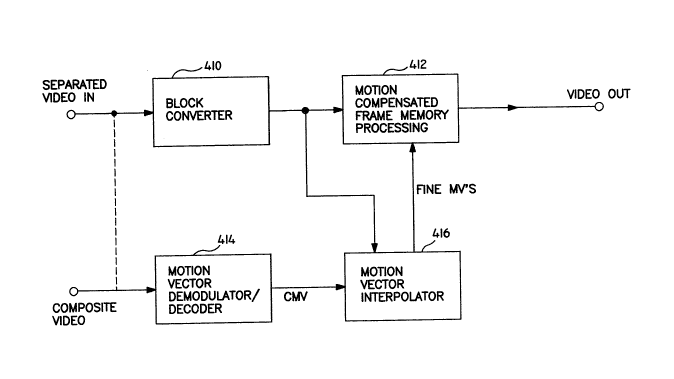
The sy8tem ~hown in Flgure 4 generallzec the
noi~e reduction cystem, de~cribed above, to other type~
of motion-compen~ated frame proce~lng sy~tem~. In thi~
sy~tem, the ~eparated video signal i~ applied to a block
converter 410 while an encoded video signal, for example,
a baseband or modulated compo~ite vldeo ~ignal, lc
applied to a motion vector demodulator and decoder 414.
As the pixels of the separated video cignal~ are being
MATA-140 - 15 ~
: : :
:~
formed into blocks of N by M pixel~, the coar~e motion
vectors which were determined for the block~ are decoded
by the circuitry 414. These coar~e motion vectore are
converted into fine motion vectors by the motion vector
interpolator 416. Finally, the fine motion vector~,
indicating the be~t local match to the current block of
pixels from the previou~ frame, are applied to the motion
compensated frame memory processing circuitry 412. As
set forth above, this circuitry may perform nolee
10 reduction or interlace to progressive ~can conversion.
In addition, if the input ~ignals to both the block
converter 410 and the motion vector decoder and
demodulator 414 are composite video ~ignal~, as indicated
by the broken line, the circuitry 412 may include a
15 motion-compensated luminance/chrominance separation
filter.
The materials presented above with reference to
Figures 3 and 4 de~cribe how the coarse motion vectors
are u~ed once they are received. The circuitry de~cribed
20 below with reference to ~lgure~ 5 through 13 deccribes
two method~ by which the coar~e motion vectors are "' ~';`'!
generated, encoded with the transmitted video ~ignal and
then decoded in a televi~ion receiver.
The first of the~e systems is de~crlbed with
25 reference to Figures 5 through 8c. This sy~tem -~
calculates motion vector~ for blocks of pixels generated,
~' .
MATA-140 - 16 - 210 7 ~
for example, by a video camera, and encodes the3e motion
vector~ with the video ~ignal u~ing Fukinuki-type
modulation.
The transmis~ion of auxiliary information in a
television ~ignal u~ing a Fukinuki carrier i9 de3cribed
in a paper by T. Fukinuki et al. entitled "Extended
Definition TV Fully Compatible With Existing Standard~",
IEE8 Transaction~ on Communications, Vol. COM-32, No. 8,
August l9B4, pp. 948-953, which is hereby incorporated by
reference for its teachings on Fukinuki-type modulation.
Thi~ paper de~cribes an area in the apatio-temporal
frequency spectrum of an interlaced color televislon
signal which contains only a relatively ~mall amount of
information that can be perceived by the human eye. Thi~
region is commonly called the Fukinuki hole.
Fukinuki modulation differs from the standard
NTSC chrominance modulation by requiring the Fukinuki
Hubcarrier ~ignal~ to be 1~0 out of pha~e from field to
flsld a~ well a~ from frame to frame and llne to llne.
For conventional chromlnance cignal guadrature
modulation, the ~ubcarrier signals are out of phace by
lBO from line to line and from frame to frame but not
from field to field.
In order to effectively separate the Fukinuki
modulated information from the compo~ite video cignal, it
MArrA-l4o - 17 - ~ 7 ~
is desirable for the information on both fields of a
given frame to be identical. This i~ true both for the
Fukinuki modulated information and for the chrominance
and high-frequency luminance information which occupies
the same band of frequencies.
An NTSC video signal image frame is made up of
525 horizontal line intervals. Thus, each field ha~
262.5 line intervals. Two type~ of field delays are
commonly used in NTSC video ~ignal processing apparatus:
a 262 H delay and a 263 H delay. Composite video ~ignals
which are delayed by 262 H have the same chrominance
subcarrier phase while signals delayed by 263 H have
oppo~ite chrominance subcarrier phase~
The Fukinuki modulated information i~
perceptually hidden in the reproduced television image
since it appears a~ flashes of complementary colors
occurring at the frame rate (i.e. 30 Hz for NTSC). These `~
fla~hes are not correlated with the image and, at wor~t,
appear to be random noi~e. Psychometric studies have
shown that the human eye i~ relatlvely in~en~itive to
image di~tortion of thi~ type since the rapldly fla~hing
complementary colorc are integrated into their
corresponding ba~e color. ~-
-.
An exemplary embodiment of the invention as
would be realized in a television studio is shown in
MATA-140 - 18 ~ 7 ~ ~ ~
Figure 5. In this Figure, a luminance signal Y i~
applied to a low-pass filter 510. The exemplary filter
510 passes luminance information having frequencie~ le~s
than 2.96 MHz to produce the output signal YL. This
signal i8 subtracted from the input luminance ~ignal Y by
the subtracter 512 to produce a high-pass filtered
luminance signal YH. The signal YH and the signal~ I and
Q are proces~ed by respective intraframe averaging
circuits 514, 516 and 518. Each of these circuits
averages corresponding pixel information from both field~
of each frame of the video signal to produce pixel values
representing the average of the pixele in each of the two
field~
. ' ,~ :,~
An exemplary intraframe averager is shown in
Figure 5a. In thi~ Figure, input camples are applied to
a delay element 550 which delays the samplec by 262
horizontal line intervals (262 H - i.e. one field
interval). The output samples provided by the delay
element 550 are summed with the input samples by an adder
552. The ~amples produced by the adder 552 are then
applied to a lH delay element 554. The output ~amples of
the lH delay element 554 are applied to one clgnal input
port of a multiplexer 556 and to a 262 H delay element
558. The other signal input port of the multiplexer 556
i~ coupled to receive the output samples provided by the ;~
262 H delay element 558. The multiplexer 556 is
re~ponsive to a control signal, FIBLD 2, to provide the
MATA-140 - 19 - 2 1~7 ~
output signal of the 1 H delay element 554 when field 2
of the input ~ignal i~ being applied to the intra-frame
averaging circuitry and to provide the output ~ignal of
the delay element 558 when field 1 i~ being applied. The
output samples produced by the multiplexer 556 are
divided by 2 (i.e. ~hifted to le~s ~ignificant bit
po~itions by 1 bit) by a divider 560. In addition to
averaging the 2 fields of each frame of video
information, the intraframe averager ~hown in Figure 5a
delays the video ~ignal~ by 263 horizontal line lnterval~
(i.e. 263 H).
Re$erring to Figure 5, the intraframe averaged
I and Q color difference signal~ provided by the circuit~
516 and 518 are next applied to a quadrature modulator ;~
525. The exemplary modulator 525 includes two digital
multiplier~ 52~ and 522, a source 524 of color ~ubcarrier
~ignal (F~c) and a circuit 521 which shifts the pha~e of
the color subcarrier signal by -90. Multiplier 520
multiplie~ the in-pha~e carrier ~ignal F~c by the Gignal
I' provided by the intraframe averaging circuit 516 to `
produce an amplitude modulated output ~ignal. 81milarly,
multiplier 522 multipliec the quadrature phace related
carrier provided by the phace-~hift circuit 521 by the Q'
color difference ~ignal, provided by the intraframe ` `
averaging circuit 518, to produce an amplitude modulated
quadrature carrier ~ignal. The output cignal~ of the
MATA-140 - 20 - 2 ~ ~7 ~ ~
multipliers 520 and 522 are combined by an adder 526 to
produce the modulated chromlnance signal C.
~'
The ~ignal C is combined with the luminance
high-freguency signal YH~ provided by the intraframe
averaging circuit 514 and with the Pukinuki modulated
-~ignal F provided, a~ described below, by the band-pass
filter 548. This combined signal repre~ents the high-
frequency components of the composite vldeo signal. It
is combined with the low-frequency components of the
luminance ~ignal provided by low-pas~ filter 510 via
compen~ating delay element 529 in an adder 530. As shown
in Figure 5, the timing signals, i.e. the horizontal and
vertical synchronization signals, the horizontal and
vertical blanking intervals and the color reference burst
signal are added to the composite video eignal by the
adder 530. The signal produced by the adder 530 is a
baseband composite video signal.
In a television studio, signals from many
different source~ are available for transmission. Since
it i9 desirable to combine the~e signals without abrupt
transitions, a common set of timing signals and a common
color ~ubcarrier signal are readily available. The
signal produced by the adder 530 is synchronized to the
other signals to be transmitted using these common
signals and the resultlng signal is applied to an RF
MATA-140 - 21 ~ 7~
modulator (not ~hown) and RF amplifiere (not shown~ to
generate a signal for broadca~t.
:.
The circuitry de~cribed above generate~ the
video ~ignal information which i~ normally sent in an
NTSC broadcast television signal. In addition, in thi~
embodiment of the invention, digital information
describlng motion vector~ for blo~k~ of pixel~ in each
frame of the video ~ignals is tran~mitted with the ;
televl~ion signal via Fukinuki-type modulation.
Briefly, this added digital information, in the
form of bit-~erial digital data, i~ converted into four- ~ ~ -
bit nibble~ which are then encoded using a 16 QAM
modulation ~cheme. Thic QAM signal is generated u~ing
Fukinuki type modulation rather than conventional ;~
quadrature amplitude modulation. The Pukinuki modulated
~ignal i~ then combined with the high-frequency luminance
and chrominance component8 of the composite video signal
a~ described above to generate a compo~ite video eignal
for tran~mi~sion.
Figure 6 ~how8 the 16 QAM ~pectrum occupied by
the motion vector data which modulates quadrature phase ~ ;
related Fukinuki carriers having a frequency Of f8c~ The ;~
bit rate selected for the data i8 al~o f~c 80 the symbol
rate, that i8 to say, the rate at which four-bit ~ymbols
are generated, i~ f~c/4~ The Fukinuki modulated data i8
MATA-140 - 22 -
transmitted only during the active video interval to
prevent any interference with synchronization ~ignal3 or
infonmation bearing ~ignals ~uch a~ teletext or gho~t
cancellation training ~ignal~ which may be ~ent during
the horizontal and vertical blanking intervale.
.~
In one video field of an NTSC signal there are ~;
240 active line~ each containing 768 pixel~, a~euming a
~ampling clock frequency Of 4f~c~ Thu~, as~uming a bit
rate Of f8c~ in the active portion of each line there are
768/4 ~ 192 bit~. Therefore, in one field interval, we
may ~end 240 * 192 = 46 080 bit~ of digital data.
Since, as de~cribed above, both field~ of the
Fukinuki modulated information within a frame are
de~irably the id0ntical, thi~ ie al~o the amount of
information that can be sent in a frame. If we ac~ume a
forward error correction overhead of approximately 25~,
the actual data bandwidth that i~ available for ~ending
motion vector information ic 46 080/1.25 - 36 e64 bit~
per frame.
Becau~e NTSC i~ transmltted on a fleld basls,
it i8 desirable to ~end motion vector~ on a field ba~
Thu~, 36 864/2 . 18 432 bitc of motion vector data may be
as~igned to each field in the NTSC image.
MATA-140 - 23 - 21~7~
Each field contains 76~ * 240 active pixels.
If the field i8 partitioned into non-overlaping motion
block~ having N pixels per line on each of M lines, then
the number of motion block~ in a field, NMB, i~ given by
equation ~2).
NMB = (768 * 240) / (N ~ M) (2)
Each motion block can, therefore, be as81gned
18 432 / NMB bits for its motion vector. If M and N are
both 12, then there are 14.4 bit~ for each motion vector. ~-
One method is to a~sign 14 bits per motion vector, seven
bit values each for horizontal and vertical, each value
having a six-bit magnitude and a one-bit ~ign. U~ing
thi~ ccheme, motion vector~ can be tran~mitted covering a
range of i64 pixel~ with 1 pixel (i.e. 70 ns) accuracy or
i32 pixelc with 0.5 pixel (35 n~) accuracy.
Figure8 8a, 8b and 8c show exemplary timing for
generating motion vector8 which are modulated onto a 16
QAM Fukinuki carrier.
Referring Figure 5, a motlon e8timator 529
provides motion vectors (Figure 8b) for each field of the
input video signal ~Figure 8a) with a delay of one field.
The~e motion vectore are provided u~ing conventional
means. For example, the motion estimator 529 may cearch
a stored frame in pixel locations defined by the celected
M~TA-140 - 24 - ~1 07~
search range (e.g. ~64 pixele) for a block of 12 by 12
pixels which exhibits the cloeest match to the current
block of pixele from the current field. The
determination of which block in the stored frame ie
- -
closest to the current frame may be made, for example,
ueing a sum of equared differencee algorithm over the
current 12 by 12 pixel block and each of the trial 12 by
12 pixel blocke from the stored frame. To preserve
spatial accuracy, it may be deeirable to ~kip alternate
lines in the blocke retrieved from the etored frame.
These motion vectors are buffered ~Figure 8c)
in a motion vector frame buffer 531 with enough storage
for motion vectore for two field~. Then, during the next
frame period, the motion vectore for both fielde are read
out twice, once during the first field period and once
during the eecond field period. Forward error correction
overhead bite are then added by circuitry 633 and the
motion vector data i~ converted into four-bit nibbles and
paeeed to the conetellation encoder 532.
In the exemplary embodiment of the inventlon,
the con~tellation encoder 532 may be a read-only memory
(ROM) whlch holde 16 four-blt value~, two blts of each
value repre~entlng an ln-phaee eignal value and two bit~
repreeenting a quadrature phase eignal value. The four-
bit signal provided by the forward error correction
coding circuitry 533 ie converted into eeparate data
MATA-140 - 25 - ~0~
values for the in-phase and guadrature signals IF and QF
which are to be u~ed to modulate ~he Fukinuki carrier.
The programming of the ROM 566 is illustrated
in Figure 5b. Thi~ Figure i~ a graphical depiction of a '~ -~
conventional 16 QAM con~tellation. Each of the X'~ in
the Figure represents a combination of two signal values,
one I and one Q, which are used to encode the 16 digital
values that may be represented by the four-bit symbols
provided by the forward error correction coding circuitry '
533. The points in the constellation may be associated
in many ways with the digital values. One exemplary
association would be to assign the points in the
constellation from the upper left corner to the lower
right corner to the successive values zero through 15.
Whatever allocation scheme is selected, it is desirably
implemented both in the transmitter and the receiver.
Thus, the con~tellation encoder 532 provides a
pair of two-bit value~, one representlng the I coordinate
of the constellation point and the other representing the
Q coordinate. As shown in Flgure,5b, each o~ the~e
values may be -1, -3, +1 or +3.
, ' ~,:,''..'~'
Returning to Figure 5, the two-bit signals IF
and QF produced by the demultiplexing and serial to
parallel converter circuitry ~32 are applied to ,~
respective pulse shaping filters 534 and 536. In the
MATA-140 - 26 2 ~ ~ 7 ~
. . ~.. .
exemplary embodiment of the invention, these filter~ are
finite impulse respon~e (FIR) filters having a raised
square root cosine frequency respon~e characteristic with
a 3 dB point at fsc/~
A combination of these filters and a similar
palr of filter~ in the receiver, described below with
reference to Figure 7, sub~ect the in-phase and
quadrature components of the 16 QAM signal to a net
raised cosine frequency response characteristic having a
6 dB point at f8C/8 and a rolloff parameter of 0.387.
This type of frequency response characteristic is
especially advantageous for 16 QAM digital modulation
systems as described in a section of a textbook by J. G.
Proakis entitled Digital Communications, McGraw/Hill,
1989, pp. 532-536, which is hereby incorporated by
reference. Using this 16 QAM modulation technique, data
values at a symbol rate of f8C/4 (8g4.9 KHz) can be
encoded with negligible inter-symbol interference.
The filtered elgnals IF' and QFI provlded by
the respective pulse shaplng fllters 534 and 536 are
applied to respective multlpliers 539 and 540.
Multiplier 538 receives the color subcarrier signal, F8C~
from source 524 via a selective phase inversion circuit
544. The circuit 544 passe~ the signal F8C during the
first field of each frame and passes an inverted (shifted
MATA-l~O - 27 - 2107~
,
.,
in phase by 180) ver~ion of the signal F~c during the
~econd field of each frame.
The modulating carrier signal applied to the
multiplier 540 ie the output signal of the selective
phase inversion circuit 544 shifted in phace by -90 by
the phase shi$ter circuit 542. Since the ~ubcarrler
signals u~ed in this embodiment of the inventlon are
digital signals having a sample rate of 4f9c~ this phase
shift operation may be implemented as a three-sample
delay element. The multipliers 538 and 540 produce the
in-phase and quadrature phase components of a Fukinuki
modulated signal. These components are combined by an
adder 546 and applied to a bandpass filter 548. The
filter 548 limits the range of frequencie~ occupied by
the Fukinuki modulated signal to 620 KHz on either side
of the color sub-carrier frequency, f~c~ As set forth
above, the Fukinuki modulated ~ignal is combined with the
other high-frequency components of the composite video
signal by the adder 528.
As described above, all o~ these high-frequency
components are identical between the two fields of each
frame. In the exemplary embodiment of the invention, the
information content of all of the high-frequency
components, i.e. the high-frequency luminance signal, YH,
the chrominance eignal comoonent C and the ~uklnuki
~'
.:
~:
MATA-140 - 28 ~ t~
modulated signal F are identical on field one and field
two of each frame.
While the information on the~e line~ i~
identical, the ~ignals are not neces~arily identical.
For the high-frequency luminance and chrominance
information, the ~ignal~ are identical between the two
fleld~. For the hlgh-frequency Fukinuki modulated
information, however, the signals on the two flelds are
oppo~ite in ~ign. Thus, when the high frequency
component~ of field one are added to the high frequency
components of field two, the Fukinuki component i9
eliminated and all that remain~ are the high-frequency
luminance and chrominance information. If one of the~e
component~ i~ subtracted from the other, the high-
frequency lumlnance and chrominance information iB lo~tand all that remaine i~ the Fukinuki modulated
information.
Thi~ is the basic function performed in the
receiver to recover both the televicion image and the
accompanying dlgital data. Figure 7 i~ a block dlagram
of exemplary circultry Yuitable for u~e ln a television
receiver. In thi~ circuitry, a digital demodulated
composite video ~ignal CV i~ applied to a low-pac~ filter
702 and to a subtracter 704. The low-pa~ filter 702
attenuate~ all csmponents of the composite video cignalc
having ~requencie~ greater than 2.96 MHz. The output - ~
.~ ~ . ,'.. ::.
, ," ~" '
,' .,:.:
:
MATA-140 - 29 - 21~7 ~ ~ ~
signal provided by the low-pas~ filter 702 i~ subtracted
from signal CV by the ~ubtracter 704 to produce an output
signal which represent~ the high-frequency components of :
the composite video ~ignal (i.e. those component~ having
frequencies greater than 2.96 MHz). Thi~ output ~ignal :~
is applied to a 262 H delay element 706 which delaye the
signal by one field interval.
The high-pase filtered ~ignal from the
subtracter 704 is added to the field delayed signal
provided by the delay element 706 in an adder 708. The
output signal produced by this adder is a combination of
the chrominance signal and high-pa~ filtered luminance
signal; the Fukinuki component has been sub~tantially
eliminated by the adder 70~. This signal is applied to a
lH delay element 712, the output signal of which is
applied in parallel to one signal input port of the
multiplexer 716 and to a 262 H delay element 714. The
output signal of delay element 714 is applied to the
other input port of the multiplexer 716. Multiplexer 716 :
is controlled by the eignal FIELD 2 to paee the output
e~gnal of the lH delay element 712 when the eecond ~ield
of each frame ie being received and the output ~lgnal of
the delay element 714 when the first field of the frame
is being received.
As described above, the high-frequency
luminance and chrominance information ie identical for
MATA-140 - 30 - ~ 9 7~
the two field~ of each frame. Thu~, the output ~ignal
produced by the adder 70~ i~ the ~um of two copies of the
identical information. Thi~ i~ the signal provided by
the multiplexer 716. Accordingly, the output terminal of
the multiplexer 716 i~ coupled to a divide-by-two circuit
71~. The signal provided by the divide-by-two c~rcuit
718 i~ the combined high-frequency luminance and
chrominance signal component~ of the input compocite
video ~ignal.
This ~ignal i8 applied to a conventional color
separation filter/color demodulator 720. Thi~ filter
which may, for example, include a ~tandard lH comb filter
separates the high freguency luminance signal component
YH and the two color-difference ~ignal component~ I and Q
from the mixed ~ignal applied to its input port u~ing
conventional techniques.
The luminance signal YH is applied to one input
port of an adder 722. The other input port of the adder
722 is coupled to receive the low-~requency luminance
~ignal Y~ provided by the low-pa~ ~ilter 702. Thl~
~ignal i~ delayed by 263 H by the delay element 723 to
compen~ate the ~ignal YL for processing delays incurred
by the ~ignal YH through the 262 H delay element 706 and
lH delay element 712.
~" , ': '
.~:
.~ ~,. .. ~.
MATA-140 - 31 - 2~ ~L~
The output signal of the adder 722, Y, is the
combined high-frequency and low-frequency lumlnance
signal~. Thi~ ~ignal and the I and Q color-difference
~ignals provided by the filter and demodulator 720 are
the separated video ~ignal which is applied to the block
converter~ 310 and 410 in the respective Figures 3 and 4,
described above.
To recover the coar~e motion vector signal,
CMV, the high-pass filtered ~ignal provided by the
subtracter 704 and its field-delayed counterpart provided
by the 262 H delay element 706 are applied to a
~ubtracter 710. This subtracter generates the difference
between the field-delayed signal and the high-pass
filtered signal provided by the subtracter 704. A~ set
forth above, when the input signal~ are the first and
second field~ of an NTSC video frame, this signal is two
time~ the 16 QAM signal which is used to modulate the
Fukinuki carrier. Thls signal is applied to a lH delay . : :
element 726 the output port of whlch 18 coupled to one
signal input port of a multlplexer 730. The other slgnal
lnput port of the multiplexer 730 is coupled to receive
the same slgnal, delayed one field interval by a 262 H
delay element 728.
The multiplexer 730 is conditioned by the
control signal FIELD 2 to pass the output ~ignal of the
lH delay 726 while the second field of a frame is being
,
M~TA-140 - 32 - 2 ~ ~ ~ 4 ~ ~
received and the output ~ignal of the 262 H delay element
728 during the next subsequent field (i.e. the fir~t
field of the next frame). Thus, the output ~ignal of the
multiplexer 730 i8 delayed by at lea~t 263 H relative to
the ~ignal CV. The output ~ignal provided by the
multiplexer i~ divided in amplitude by two by a divide-
by-two circuit 732 to generate a ~ignal, P', which i~
applied to a 16 QAMidemodulator 734. Thls demodulator,
which is described below with reference to Figure 7a,
recovers the four-bit digital data from the 16 QAMi~lgnal
provided the d~vide-by-two circuit 732.
As described above, the digital information
encoded in the two field~ of each frame i9 identical.
Thus, circuit 736 proce~es the digital data to eliminate
lS the redundant data in the second field of each frame and
to reformat the data from the four-bit nlbbles which were
decoded from the 16 QAM ~ignal into 14-bit coarae motion
vectors.
~.
Since only the dlgltal data from the firct
field is pa~8ed as valld data, it le contemplated that
the 262 H delay element and multiplexer 730 may be
eliminated without affecting the performance of the
digital receiver. In this instance, the data decoded by
the 16 QAM demodulator 736 during the ~econd field of
each frame is not merely redundant but erroneou~ 6ince it ; ~ -
MATA- 14 0 - 3 3 - 2 3L ~3 7 ~
represent~ pixel difference value~ taken between fielda
of different frames.
Figure 7A i8 a block diagram of an exemplary 16 `~
QAM demodulator ~uitable for u~e as the circuit 734,
~hown in Figure 7. In this circuit, the ~ignal F~
provided by the divide-by-two circui~. 732 is applied to
two multiplier~ 740 and 742. The other input port of the
multiplier 740 is coupled to receive the color subcarrier
signal FBC'- Multiplier 742 receives a 90 phase-shifted
version of this signal from a phase shifter 741. The
multipliers 740 and 742 demodulate the quadrature-
modulated information to provide the s~gnal~ If~' and ;~
Qf~ which are substantially the same as the signals I
and Qf' of Figure 5. These signals are applied to
respective pulse-shaping filters 744 and 746.
: .
As de~cribed above, the filters 744 and 746
apply raised square root cosine frequency response
characteristics to the respective signals If" and Qf" .
The two-bit output 8ignal~ provided by the ~ilter8 744
and 746 are applied to the addre~s lnput port o~ a ROM
748. The ROM 748 is responslve to a clock signal having
a frequency fBC to load the combined address value at an
appropriate time and to reproduce the encoded digital
data. While the pulse-shaping filters 744 and 746 may be ~-
2s identical to the filters 534 and 536 of Figure 5, the ROM
748 is programmed as the inverse of the constellation
MATA-140 - 34 - 21~741~
encoder 532 ~hown in Figure 5. Thu~, the ROM 748
produces four-bit output signals in respon~e to input
value~ representing point~ in the 16 QAM constellation
shown in Figure 5b. As described above, these four-bit
values are converted into 14 bit motion vector~ by the
circuitry 736. This circuitry may include, error
correction decoding circuitry (not shown) which removes
the forward error correction bits that were inserted by
the circuitry 533 of Figure 5, and reformatting circuitry
(not shown) which combines successive bits provided by
the error correction decoding circuitry to regenerate the
14-bit motion vectors.
An alternative method of conveying motion ;~
vector information from a studio to a consumer television
receiver i8 shown in Figures 9 through 13. This method
encodes the motion vector data using 16 QAM modulation
onto a 8uppressed subcarrier which, in turn, modulates a
a carrier which i9 in quadrature with the picture carrier ;~
of the modulated televl~lon slgnal.
Referrlng to Flgure 9, the component video
signal (Figure 9a) in the televi~ion studio is applied to
a motion e~timator 910. Thi~ estimator may be identical
to the motion estimator 529, described above with ;~
reference to Figure 5. As shown in Figure 9b, the motion
estimator 910 produces motion vectors with a delay of one
field interval. The~e motion vectors are applied to
M~TA-140 - 35 - ~
forward error correction coding circuitry 914, which may
be identical to the circuitry 533, de~cribed above. The
output signal of the error correction circuitry 914
(Figure 9c) i~ applied to a 16 QAM modulator 916. This
modulator includes a constellation encoder (not shown)
which may be identical to the encoder 532, de~cribed
above, two pulse shaping filters (not shown), two
multipliers (not ~hown), a 90 phase shift clrcuit ~not
shown) and a summing circuit (not shown) which may be
similar to the respective pulse shaping circuits 534 and
536, multipliers 538 and 540 and adder 546, described
above. Since, in this second embodiment of the
invention, ordinary quadrature modulation i8 u~ed instead -~
of Fukinuki-type modulation, there i8 no circuitry that
is analogous to the phase invert circuit 544.
The only other differences between the 16 QAM
modulators shown in Figures 5 and 9 are the frequency
response characteristic of the pulse shaping filters and
the frequency of the QAM carriere. These differences are
both illustrated in Figure 11. A~ ~hown in Figure 11,
the 16 QAM carrier~ have a freguency f f8C/5 and the
pulse chaping filters in both the studio and the consumer
receiver control the frequency spectrum of each of the
in-phase and quadrature phase signals to occupy a band of
frequencies f8C/8 on either side of the f8c/5 carrier.
The pulse shaping filters used in this QAM modulator and
in the corresponding QAM demodulator in the receiver are
MATA-140 - 36 - 21~7~1~
square-root rai~ed cosine filter~ which, when combined
have a 3dB point at f8C/8 and a roll off factor of 10~.
The output eignal of the 16 QAM modulator 916,
ehown in Figure 9, i~ the signal Sub Signal, which i~
applied to a multiplier 1012, shown in Figure 10. The
main video ~ignal, lncluding the conventlonal luminance
and chrominance componentc, in ba~eband form i~ applied
to another multiplier 1010. The multiplier~ 1010 and
1012 are coupled to receive recpective quadrature-phase
related ~ignal~ at the frequency of the radio frequency
(RF) carrier signal which i~ modulated by the video `
~ignal. In Figure 10, the RF carrier i~ provided by a
signal ~ource 1014 and the quadrature phase carrier ie
provided by a 90 pha~e ~hift circuit 1016. -
: ~ .
The output ~ignal of the multiplier 1010 iB
applied to a veetigal ~ide band (VSB) filter 1018. The
filter 1018 limit~ the lower ~ideband of the modulated
vldeo ~ignal to 1.25 MHz below the RF carrler ~requency
whlle allowlng the upper ~ldeband to occupy a range of
frequencie~ 6 MHz above the RF carrler frequency. The
range of frequencies which may be occupied by thic signal
i~ illustrated in Figure 12a where the RF carrier
frequency i~ repre~ented a~ PC. ~ ~ -
.-, ~., .
The output ~ignal of the multiplier 1012 i~
applied to an inver~e Nyquict filter. Figure 12b
~.-,~- . '-
.. .~..
MATA-140 - 37 - 2107~1~
illustrate~ the range of frequencie~ which may be
occupied by the ~ignal provided by the multiplier 1012.
This i~ a double ~ideband ~ignal centered about the
frequency, PC, of the RF carrier. Figure 12c illu~trate~
the effect of applying the ~ignal to the Inver~e Nyqui~t
filter frequency re~pon3e characteri~tic 1210. In thi~
frequency ~pectrum, the upper cideband MCMV+ i~ reduced
in amplitude relative to the lower ~ideband ~ignal MCMV-.
The output eignal~ of the vectigal sideband -
filter 1018 and the inver~e Nyqui~t filter 1020 are
combined in a ~umming circuit 1022 to produce a ~ignal
having the compo~ite frequency ~pectrum ~hown in Figure
12d. Thi~ i~ the ~ignal which i~ tran~mitted from the
studio and received at the con~umer receiver.
Figure 13 1~ a block diagram of a con~umer
televi~ion receiver which ic adapted to receive thic
television ~ignal. In this receiver, the video ~ignal ic
~upplied by antenna 1300 to an RP amplifier 1310 which
ampllfles the received clgnal and pa~ec lt to a mixer
1312. The mlxer 1312 heterodynec the RF ~ignal with an
internally generated o~cillatory ~ignal (not ehown) to
generate a modulated video ~ignal having an intermediate
frequency (IF) carrier. This cignal i~ applied to an IF
amplifier 1314 which typically include~ a Nyquiet filter
1316.
MATA-140 - 38 - 2~7~4
Figure 12e shows the band of frequencies that
may be occupied by the signal produced by the Nyqui~t
filter 1316. The frequency axis in this Figure is
oppo~ite from the other Figures, increasing to the left,
to simplify comparison of the frequency spectra of the
transmitted and received signals. As is well known, the
heterodyning process performed by the mixer 1312 reflects
the frequency components about the IF carrier frequency ~;
relative to the RF carrier frequency.
As shown in Figure 12e, the band of frequencies `~
occupied by the 16 QAM modulated video signale i~
substantially symmetric about the IF carrier frequency
and greatly reduced in amplitude with respect to the
information-bearing video ~ignals. This reduction in the
amplitude o$ the quadrature IF carrier reduces the
visibility of the modulated digital data in television
receivers which do not synchronously demodulate the video
signal.
In the televlslon receiver lllustrated in
Flgure 13, however, the vldeo signal is synchronously ;~
demodulated. This is accomplished by applying the signal
provided by the Nyquist filter 1316 to an IF carrier - ;
phase-locked loop (PLL) 1318 and to two multipliers 1320
and 1322. The PLL 1318 generates a signal at the IF
frequency which is locked in phase to the RF carrier that
wa~ used to modulate the slgnal at the studio. Thls IF
...~ ~ . ,. .~ .
~'.'
MATA-140 - 39 - 2~7~
carrier ~ignal is applied to the multiplier 1320 directly
and to the multiplier 1322 through a 90 pha~e ~hift
circuit 1324. The output signal of the multiplier 1320 : :
is the in-phase component of the video signal while the
output signal of the multiplier 1322 is the quadrature- : ~:
pha~e component. These signals are then pae~ed through a
gho~t cancellation filter 1326, which may, for example,
operate in the ~ame manner at the filter descrlbed in
U.S. Patent No. 4,864,403 entitled ADAPTIVE TELEVISION
GHOST CANCELhATION SYSTEM INCLUDING FILTER CIRCUITRY WITH - ;
NON-INTEGER SAMP~E DE~AY, which i~ hereby incorporated by ~ .
reference for its teaching on the elimination of
multipath di~tortion.
The in-pha~e component of the gho~t
cancellation filter 1326 i~ applied to eynchronization
~ignal separation circuitry 1328 which generate~
horizontal and vertical synchronization cignals H9 and VS
and a bur~t gate signal, BG, which i~ applied to an f8c/5
P~ 1330. The PLL 1330, which ic also coupled to receive
the in-phase ~ignal provided by the ~ilter 1326, may be
implemented ac a 4~9c P~ having a frequency divide-by-
twenty circuit to generate the f~c/5 cignal from the 4f~c
~ignal.
The output ~ignal of the PLL 1330 and the
quadrature output signal of the ghost cancellation filter
1326 are applied to a 16 QAM demodulator 1332. The
MATA-140 - 40 - ~ ~ 7 ~ ~ ~
demodulator 1332 operates in the ~ame manner a~ the 16
QAM demodulator ~hown Figure 7a except that the carrier
signal applied to the multipliers (not ~hown) which
correspond to the multiplier~ 740 and 742 has a frequency
of f~c/5 in~tead f f8C and the pulse ~hape filters (not
shown) which correspond to the filters 744 and 746 have a : .
square-root raised co~ine frequency response
characteri~tic which matches the frequency response ~ .
characteri~tic of the pulse ~haping filtere (not ~hown) ~ :
u~ed in the 16 QAM modulator 916, described above with
reference to Figure 9.
. ,,:: -:,;
.: ;:
The output signal of the 16 QAM demodulator
1332 i~ the coar~e motion vector signal, CMV, shown in
Figure~ 3 and 4. The separated video signal shown in
Figures 3 and 4 may be generated by applying the in-phase ~ ;
output signal of the gho~t cancellation filter 1326 to a ~.
conventional luminance/chrominance separation circuit
1334, as shown in Figure 13.
:,.
Whlle the precent lnventlon hac been described
in terms of two exemplary embodiments, it 1~ contemplated
that it may be practiced a~ outlined above within the
spirit and scope of the appended claims. :.
: ~- ~, .