Note: Descriptions are shown in the official language in which they were submitted.
WO 92/18980 PCT/US92/02194
-1-
A SINGLE TRANSISTOR NON-VOLATILE ELECTRICALLY
ALTERABLE SEMICONDUCTOR MEMORY DEVICE
This application is a continuation-in-part
application of a co-pending application 07/467,907
filed on January 22, 1990.
Technical Field
The present invention relates to a single
transistor electrically programmable and erasable
memory device.
Background Of The Invention
Non-volatile electrically alterable
semiconductor memory devices are well-known in the
art. See, for example, U.S. Patent No. 4,203,158.
In such a device, electrical alterability is achieved
by Fowler-Nordheim tunneling of charges between a
floating gate and the silicon substrate through a
very thin dielectric. Typically, the thin dielectric
is an oxide layer with a thickness of less than 100
angstroms. However, such a device requires a
floating gate transistor and a separate select
transistor. for each storage site. Thus, necessarily,
each storage site or cell is large due to the number
of transistors required for each cell. Further,
another disadvantage is the reliability and
manufacturability problem associated with the thin
oxide tunnel element between the substrate and the
' f loating gate .
U.S. Patent Nos. 4,274,012 and 4,599,706 seek to
overcome the problem of reliability and manufac-
turability of the thin oxide tunnel element by
storing charges on a floating gate through the
mechanism of Fowler-Nordheim tunneling of charges
WO 92/18980 PCT/US92/02194
-2-
between the floating gate and other polysilicon
gates. The tunneling of charges would be through a
relatively thick inter-polyoxide. Tunneling through
thick oxide (thicker than the oxide layer disclosed
in U.S. Patent No. 4,203,158) is made possible by the
locally enhanced field from the asperities on the
surface of the polycrystalline silicon floating gate.
Since the tunnel oxide is much thicker than that of
the tunnel oxide between the floating gate and the
substrate, the oxide layer is allegedly more reliable
and manufacturable. However, this type of device
normally requires three layers of polysilicon gates
which makes manufacturing difficult. In addition,
voltage during programming is quite high and demands
stringent control on the oxide integrity.
Electrically programmable devices which are
alterable by application of ultraviolet light
treatment, typically known as EPROM devices, are
well-known in the art. However, erasure requires
erasure of the entire memory device by application of
UV light.
Hot electron injection has been proposed by Dill
and Toombs in 1969 on an MNOS structure (Vol. 12,
Solid State Electronics) to improve switching speed
and to reduce the need for a separate select
transistor for each cell in a memory array.
Recently, U.S. Patent No. 4,698,787 discloses a
device that is programmable as if it were an EPROM
and erasable like an EEPROM. Although such a device
~ requires the use of only a single transistor for each
cell, it is believed that it suffers from the
requirement of high programming current which makes
it difficult to utilize on-chip high voltage
generation for programming and erasing. Further, it
is believed that such a device requires tight
-3- 2~o~s~s
distribution program/erase thresholds during device operation,
which results in low manufacturability yield.
Summary Of The Invention
In accordance with the present disclosure, an
electrically programmable and erasable memory device is
disclosed. The memory device has a plurality of storage
sites. A plurality of row address lines, a plurality of
column address lines, and a common line is supplied to the
plurality of storage sites. Each combination of one of the
plurality of row address lines and one of the plurality of
column address lines defines a different one of the plurality
of storage sites. Each of the storage sites comprises a
single transistor that has a source coupled to the common
line, a drain coupled to an associated one of the plurality of
column address lines and a control gate coupled to an
associated one of the plurality of row address lines. A
floating gate is positioned between the control gate, the
source and the drain and is capacitively coupled to the
source. Means for injecting hot electrons generated by abrupt
potential drop onto the floating gate is provided. The
associated ones of the row address lines and the common line
are raised to a first predetermined potential above that of
the associated column address line, with the potential applied
to said common line being above the potential applied to said
associated one of the row address lines. Finally, means for
inducing Fowler-Nordheim tunneling of charges from the
floating gate to the control gate is also provided. The
associated row address line is raised to a second
66810-736
r'
w_. 21 p767fi
- 3a -
predetermined potential above the associated column address
line.
In accordance with the present invention there is
provided an electrically programmable and erasable memory
array device comprising: a substrate of semiconductor
material of a first conductivity type; a plurality of storage
sites, each being a single asymmetrical transistor and
comprising: first and second spaced-apart regions in said
substrate with a channel region therebetween, said first and
second regions are of a second conductivity type; a first
insulating layer disposed over said substrate including over
said first, second and channel regions; an electrically
conductive floating gate disposed over said first insulating
layer and extending over a portion of said channel region and
over a portion of said second region to maximize a capacitive
coupling therewith; a second insulating layer disposed over
and adjacent said floating gate and having a thickness
permitting Fowler-Nordheim tunneling of charges therethrough;
an electrically conductive control gate having two
electrically connected sections, a first section disposed over
said first insulating layer, spaced apart from said floating
gate and adjacent to said second insulating layer, extending
over a portion of said first region; said second section
disposed over said second insulating layer to minimize
capacitive coupling with said floating gate; a plurality of
row address lines; a plurality of column address lines; a
single common line; and said plurality of storage sites
arranged in an array of rows and columns with said first
66810-736
21p7fi76
- 3b -
region of each storage site in the same column electrically
connected to the same one of said plurality of column address
lines; and with said second region of all the plurality of
storage sites electrically connected to said common line; and
with said control gate of each storage site in the same row
electrically connected to the same one of said plurality of
row address lines.
In accordance with the present invention there is
further provided a method of reading a select storage site
from an electrically programmable and erasable memory array
device having a plurality of storage sites, said device having
a substrate of semiconductor material of a first conductivity
type, with each storage site including a single asymmetrical
transistor, with each transistor having first and second
spaced-apart regions in said substrate with a channel region
therebetween, said first and second regions are of a second
conductivity type; a first insulating layer disposed over said
substrate including over said first, second and channel
regions; an electrically conductive floating gate disposed
over said first insulating layer and extending over a portion
of said channel region and over a portion of said second
region to maximize a capacitive coupling therewith; a second
insulating layer disposed over and adjacent said floating gate
and having a thickness permitting Fowler-Nordheim tunneling of
charges therethrough; an electrically conductive control gate
having two electrically connected sections, a first section
disposed over said first insulating layer, spaced apart from
said floating gate and adjacent to said second insulating
66810-736
~,,,~~=
21 p7fi76
- 3c -
layer, extending over a portion of said first region; said
second section disposed over said second insulating layer to
minimize capacitive coupling with said floating gate; said
method comprising: applying a ground potential to the second
region of each transistor of all the storage sites; applying a
first positive potential to the first region of each
transistor of a first plurality of the storage sites, said
first plurality being less than all of the storage sites but
including at least said select storage site; applying a second
positive potential to the control gate of each transistor of a
second plurality of storage sites, said second plurality being
less than all of the storage sites and having at least said
select storage site in common with said first plurality; and
sensing the current passing through the transistor at the
select storage site in said first plurality in common with
said second plurality.
In accordance with the present invention there is
further provided a method of programming a select storage site
from an electrically programmable and erasable memory array
device having a plurality of storage sites, said device having
a substrate of semiconductor material of a first conductivity
type, with each storage site including a single asymmetrical
transistor, with each transistor having first and second
spaced-apart regions in said substrate with a channel region
therebetween, said first and second regions are of a second
conductivity type; a first insulating layer disposed over said
substrate including over said first, second and channel
regions; an electrically conductive floating gate disposed
66810-736
21 p7fi7fi
- 3d -
over said first insulating layer and extending over a portion
of said channel region and over a portion of said second
region to maximize a capacitive coupling therewith; a second
insulating layer disposed over and adjacent said floating gate
and having a thickness permitting Fowler-Nordheim tunneling of
charges therethrough; an electrically conductive control gate
having two electrically connected sections, a first section
disposed over said first insulating layer, spaced apart from
said floating gate and adjacent to said second insulating
layer, extending over a portion of said first region; said
second section disposed over said second insulating layer to
minimize capacitive coupling with said floating gate; said
method comprising: applying a first positive potential to the
second region of each transistor of all the storage sites
including a plurality of transistors from storage sites not
selected for programming; applying a ground potential to the
first region of each transistor of a first plurality of the
storage sites, said first plurality being less than all of the
storage sites but including at least said select storage site;
and applying a second positive potential, less than the first
positive potential, to the control gate of each transistor of
a second plurality of storage sites, said second plurality
being less than all of the storage sites and having at least
said select storage site in common with said first plurality;
whereby the transistor at the select storage site in said
first plurality in common with said second plurality is
programmed.
In accordance with the present invention there is
66810-736
21 p7676
- 3e -
further provided a method of programming and reading a select
storage site from an electrically programmable and erasable
memory array device having a plurality of storage sites, said
device having a substrate of semiconductor material of a first
conductivity type, with each storage site including a single
asymmetrical transistor, with each transistor having first and
second spaced-apart regions in said substrate with a channel
region therebetween, said first and second regions are of a
second conductivity type; a first insulating layer disposed
over said substrate including over said first, second and
channel regions; an electrically conductive floating gate
disposed over said first insulating layer and extending over a
portion of said channel region and over a portion of said
second region to maximize a capacitive coupling therewith; a
second insulating layer disposed over and adjacent said
floating gate and having a thickness permitting Fowler-
Nordheim tunneling of charges therethrough; an electrically
conductive control gate having two electrically connected
sections, a first section disposed over said first insulating
layer, spaced apart from said floating gate and adjacent to
said second insulating layer, extending over a portion of said
first region; said second section disposed over said second
insulating layer to minimize capacitive coupling with said
floating gate; said method comprising: programming said
select storage site by: applying a first positive potential
to the second region of each transistor of all the storage
sites including a plurality of transistors from storage sites
not selected for programming; applying a ground potential to
66810-736
21 p7676
- 3f -
the first region of each transistor of a first plurality of
the storage sites, said first plurality being less than all of
the storage sites but including at least said select storage
site; applying a second positive potential, less than the
first positive potential, to the control gate of each
transistor of a second plurality of storage sites, said second
plurality being less than all of the storage sites and having
at least said select storage site in common with said first
plurality; whereby the transistor at the select storage site
in said first plurality in common with said second plurality
is programmed; and reading said select storage site by:
applying a ground potential to the second region of each
transistor of all the storage sites; applying a first positive
potential to the first region of each transistor of a first
plurality of the storage sites, said first plurality being
less than all of the storage sites but including at least said
select storage site; applying a second positive potential, to
the control gate of each transistor of a second plurality of
storage sites, said second plurality being less than all of
the storage sites and having at least said select storage site
in common with said first plurality; and sensing the current
passing through the transistor at the select storage site in
said first plurality in common with said second plurality.
,.~' ,< 66810-736
WO 92/18980 PCT/US92/02194
-4-
Rr;ef Description Of The Drawinas
Fig. 1 is a cross-sectional side view of a
single transistor non-volatile electrically alterable
memory cell.
Fig. 2 is a schematic diagram of a memory device
using an array of the memory cells shown in Fig. 1.
Fig. 3(a-i) are cross-sectional side views of
the memory cell of Fig. 1, showing the steps in a
method of making a recrystallized floating gate of
the memory cell.
Fig. 4(a-l...s-1), 4(a-2...s-2), and 4(a-3...
s-3) are cross sectional side views in the cell
height direction, through the stack-gate region, and
through the source region, respectively, of the
memory cell of Fig. 1, showing the steps in a method
of making the memory cell.
Detailed Description Of The Drawings
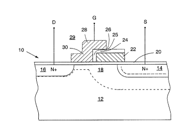
Referring to Fig. 1, there is shown a single
transistor non-volatile electrically alterable
semiconductor memory cell 10. The cell 10 comprises
a semiconductor substrate 12, such as silicon. The
substrate 12, in one embodiment, can be a P-type
silicon substrate with a typical doping level range
from 5 to 50 ohm-cm, depending on the level of
scaling. (A more detailed description of the method
of manufacturing the cell 10 will be discussed
hereinafter.)
Within the substrate 12 are defined drain region
16 and source region 14 with a channel region 18
therebetween. Disposed over the drain region 16,
channel region 18, and source region 14 is a first
layer 20 of insulating material, on the order of 70-
200 angstrom of thickness. The first layer 20 can be
WO 92/18980 PCT/US92/02194
-5-
an insulating material made from silicon dioxide,
silicon nitride or silicon oxynitride. Disposed over
the first layer 20 is a floating gate 22. The
floating gate 22 is positioned over a portion of the
channel region 18 and over a portion of the source
region 14. The floating gate 22 can be a polysilicon
gate and in one embodiment is a re-crystallized
polysilicon gate. A second insulating layer 25 has a
first portion 24 disposed over the floating gate 22
and a second portion 26 disposed adjacent to the
floating gate 22. The first portion 24 (top wall 24)
of the second layer 25 is an insulating material and
can be silicon dioxide, silicon nitride or silicon
oxynitride and is on the order of 1000-3000 angstrom
in thickness. The second portion 26 (side wall 26)
of the second layer 25 is also of an insulating
material and can be silicon dioxide, silicon nitride
or silicon oxynitride and is on the order of 150-
1200 angstrom in thickness. A control gate 29 has
two portions: A first portion 28 is disposed over
the top wall 24 of the second layer 25; a second
portion 30 is disposed over the first layer 20 and is
immediately adjacent to the side wall 26 of the
second layer 25. The second portion 30 of the
control gate 29 extends over a portion of the drain
region 16 and over a portion of the channel region
18.
The dimensions of the cell 10 depend upon the
process used. Thus, the foregoing dimensions for the
~ first layer 20, side wall 26, and top wall 24 are
only illustrative examples. Further, the material
for the first layer 20 and the second layer 25 are
also illustrative examples only. In general,
however, the dimensions of the cell 10 must be such
that electrons emanating from the drain region 16 are
WO 92/18980 PCT/US92/02194
-6-
injected onto the floating gate 22 by sensing an
abrupt potential drop. (The specific mechanism of
the theory of operation of the cell 10 will be
explained in greater detail hereinafter.) Further,
the dimensions of cell 10 must be such that charges
from the floating gate 22 are removed by tunneling
through the Fowler-Nordheim mechanism through the
second layer 25 onto the control gate 29. The
particular manner of operating the cell 10 is as
follows:
Initially, when it is desired to erase cell 10,
a ground potential is applied to the source 14 and to
the drain 16. A high-positive voltage, on the order
of +15 volts, is applied to the control gate 29.
Charges on the floating gate 22 are induced through
the Fowler-Nordheim tunneling mechanism to tunnel
through the second layer 25 to the control gate 29,
leaving the floating gate 22 positively charged.
When selective cells 10 are desired to be
programmed, a ground potential is applied to the
drain region 16. A positive voltage level in the
vicinity of the threshold voltage of the MOS
structure defined by the control gate 29, (on the
order of approximately of +1 volt), is applied to the
control gate 29. A positive high voltage, on the
order of +12 volts, is applied to the source region
14. Electrons generated by the drain region 16 will
flow from the drain region 16 towards the source
region 14 through a weakly-inverted channel region
~ 18. When the electrons reach the region where the
control gate 29 meets the side wall 26, the electrons
see a steep potential drop approximately equal to the
source voltage, across the surface region defined by
the gap of the side wall 26. The electrons will
accelerate and become heated and some of them will be
WO 92/18980 PCT/US92/02194
~Z ~_ ~i ~,
_, _
injected into and through the first insulating layer
20 onto the floating gate 22.
The injection of electrons onto the floating
gate 22 will continue until the charged floating gate
22 can no longer sustain a high surface potential
beneath, to generate hot electrons. At that point,
the electrons or the negative charges in the floating
gate 22 will decrease the electron flow from the
drain region 16 onto the floating gate 22.
Finally, in a read cycle, ground potential is
applied to the source region 14. Conventional
transistor read voltage, such as +2 volts and +5
volts, are applied to the drain region 16 and to the
control gate 29, respectively. If the floating gate
22 is positively charged (i.e., the floating gate is
discharged), then the channel region 18 directly
beneath the floating gate 22 is turned on. When the
control gate 29 is raised to the read potential, the
region of the channel region 18 directly beneath the
second portion 30 is also turned on. Thus, the
entire channel region 18 will be turned on, causing
electrical current to flow from the source region 14
to the drain region 16. This would be the "1" state.
On the other hand, if the floating gate 22 is
negatively charged, the channel region 18 directly
beneath the floating gate 22 is either weakly turned
on or is entirely shut off. Even when the control
gate 29 and the drain region 16 are raised to the
read potential, little or no current will flow
' through the portion of the channel region 18 directly
beneath the floating gate 22. In this case, either
the current is very small compared to that of the "1"
state or there is no current at all. In this manner,
the cell 10 is sensed to be programmed at the "0"
state.
WO 92/18980 PCT/US92/02194
_g_
Referring to Fig. 2, there is shown a memory
device 40. The memory device 40 has an array 50 of
memory cells. The peripheral circuitry on the
device 40 includes conventional row address decoding
circuitry 52, column address decoding circuitry 42,
sense amplifier circuitry 44, output buffer circuitry
46 and input buffer circuitry 48. These conventional
circuits correspond to the peripheral devices of the
prior art.
The interconnection of the source, drain and
gate of each of the cell 10 to the memory array 50 is
as follows: All of the source 14 of each of the
memory cell 10 are connected to the other through a
common source line. The drain 16 of each of the cell
10 in the same column are connected together. Thus,
column 18a has connected thereto the drain from each
of the cell 10 in the leftmost column. The plurality
of columns 18(a...z) are connected to the column
address decode 42. The gate 29 of each of the memory
cells 10 in the same row are connected together.
Thus, the row signal line 62a connects to the gate 29
of each of the memory cells 10 in the uppermost row.
The plurality of rows 62(a...z) are supplied to the
row address decode 52.
In the operation of the memory array 50, in the
event an erased mode is desired, the plurality of
column address lines 18(a...z) are all brought to a
ground potential. The common source line 14 is also
brought to a ground potential. The plurality of row
' address lines 62(a...z) are all brought to a high
positive potential, such as +15 volts. In this
manner, all of the memory cells 10 in the memory
array 50 are erased. When only a selected row of the
memory array 50 is to be erased, the particular row
address line, e.g., 62m, is raised to a high positive
WO 92/18980 PCT/US92/02194
r, rs
2~.~
_g_
potential, such as +15 volts with the rest of the row
addresses at ground potential. In this manner only
the memory cells in row 62m are erased.
Thereafter, for selective programming of
selected memory cells 10, programming is accomplished
as follows: The column address line 18a is brought
to ground potential or a low potential between, for
example, ground and 1.0 volt. The particular row
address line 62m, which is connected to the gate 28
of the particular memory cell 10 to be programmed is
brought to a +1 volt, or higher depending upon the
voltage of the column address line 18a. The
unselected row address lines 62(a...l,n...z) are
brought to a ground potential. The common source
line 14 of the memory array 50 is brought to a high
positive potential, such as +12 volts. The
unselected column lines 18(a...l, n...z) are brought
to a high potential, such as +5 volts.
The voltage supplied to the various contacts of
the selected memory cell 10 are as follows: Source
14 is brought to a +12 volts, drain 16 is brought to
a potential, between ground and +1.0 volt, and gate
28 is brought to +1 to +2 volt. This causes
programming of the selected memory cell 10, as
previously discussed.
The voltage supplied to the unselected memory
cell 10 can have the following possible voltage
potentials supplied thereto: For all of the memory
cells in the selected row 62m, the drain 16 is at +5
' volts, the source 14 is at +12 volts, and the gate is
at +1 to +2 volts. In this condition, since the gate
28 is at a potential much less than the potential of
the drain 16 and the source 14, electrons will not
migrate from the drain 16 through the channel region
WO 92/18980 PCT/US92/02194
-10-
18, beneath the control gate 29, onto the floating
gate 22.
For all of the memory cells 10 in the same
column 18m as the selected memory cell 10., the
voltage potential applied to the various regions are
as follows: Drain 16 is at a potential between
ground and +1 volt, source 14 is at +12 volts, the
control gate 28 is at ground potential. In this
configuration, although the source 14 is at a higher
positive potential than the drain 16, there is no
induced channel beneath the control gate 28. Thus,
there is no flow of electrons from the drain 16 to
the control gate 28 and through the first insulating
layer 20 to the floating gate 22.
Finally, with respect to the memory cells that
are not in the_same row 62m or in the same column 18m
as the selected memory cell 10, the voltage potential
applied to the various regions of the memory cell 10
are as follows: +12 volts to the source 14, ground
potential to the gate 28 and +5 volts to the drain
16. In this configuration, of course, no electron
flow occurs at all.
Finally, when a read operation is desired, the
common source line 14 is brought to a ground
potential. The selected column address line 18m,
supplied to the selected memory cell 10, is brought
to a +2 volts. The selected row address line 62m,
connected to the selected memory cell 10, is brought
to a +5 volts. The selected memory cell 10 can thus
~ be read out.
Theory Of Operation
If we assume the substrate 12 is to be of P-
type conductivity and the source region 14 and the
WO 92/18980 PCT/US92/02194
-11-
drain region 16 to be N-type conductivity, then the
following occurs.
Erase
The source region 14 and the drain region 16 are
supplied with equal potential and at a reference
potential, for example, ground potential. The
control gate 29 is raised to a predetermined
potential V, above the reference potential supplied to
the source 14 and the drain 16. The strong coupling
from the floating gate 22 to the body 12 and source
14 will cause a high voltage drop between the
floating gate 22 and the control gate 29. This
voltage drop will, in turn, cause electrons to tunnel
from the floating gate 22 to the control gate 29 by
the mechanism of Fowler-Nordheim tunneling. This
tunneling occurs due to the locally-enhanced field on
the surface of the floating gate 22. The local
enhancement of the electric field can be due to the
unsmoothed grain size of the floating gate 22, or
asperity on the floating gate 22, which is typically
made of polysilicon. It can also be due to a
purposely created sharp edge on the floating gate 22
through properly designed process. Once the positive
charges are gradually built up on the floating gate
22; i.e., electrons are tunneled away from the
floating gate 22 onto the control gate 29, the
voltage potential drop between the floating gate 22
and the control gate 29 will continue to decrease
' until the potential drop can no longer sustain a
significant amount of Fowler-Nordheim tunneling. At
this final voltage drop between the control gate 29
and the floating gate 22, which is labelled VX, the
total positive charge +Q=8 on the floating gate 22 can
WO 92/18980 PCT/US92/02194
-12-
be estimated to a first order by the following
equation:
+Qfg - ( Ve - V: Via ) * ( Cfc + Cfb + Cfs )
where
Cfc is the capacitance between the floating gate
22 and the control gate 29;
C~ is the capacitance between the floating gate
22 and the body 12;
Cfs is the capacitance between the floating gate
22 and the source 14; and
Vie - Ve*Cfc~ (Cfe + Cfb + Cfs)
is the initial floating gate potential when it is
free from charge .
Va is the erase voltage.
If Cfc is much smaller than the total floating
gate capacitance (Cfc + Cn, + Cfa) , then Via is quite
small compared to V, and Vx. Thus, the positive
floating charge can be approximated by
+~fs - ( Ve - Vx ) * ( Cfc + Cfb + Cfs )
In fact, in a preferred embodiment, it is desired to
minimize Cfc and maximize Cfs. Thus, the amount of the
second portion 28 of the control gate 29 over the
second insulating layer 25 should be minimized.
Similarly, the amount of the floating gate 22
directly over the source 14 is maximized.
Program
After the cell 10 is erased and the floating
gate 22 is positively charged, the drain region 16
' and the control gate 29 are maintained at the ground
potential, or slightly above, such as +1.5 volts.
The voltage potential supplied to the source 14 of
the selected memory cell 10 is raised to a
predetermined potential VP above ground potential.
The induced surface charge underneath the floating
WO 92/18980 PCT/US92/02194
-13-
gate 22 will propagate the source potential along the
induced channel under the floating gate 22 to the
region where the floating gate 22 meets the side wall
26. The floating gate 22 is nearly at a potential
given by the following equation:
Vfa = (Qta + Cfs*Vp + Cn,*Vp) / (C=~ + C~ + Cts)
where Vp is the programming voltage.
If the control gate 29 is raised to a potential
VL, slightly above the drain potential and is near the
threshold voltage, such that the channel region 18
directly beneath the control gate 29 is slightly on,
the sub-threshold electron current will begin to flow
from drain 16 towards source 14. The current will
flow through the weakly-inverted channel. When the
electron reaches the region where the first portion
30 of the control gate 29 meets the side wall 26 of
the second insulating layer 25, the electrons see a
steep potential drop, approximately equal to the
source voltage, across the surface region defined by
the gap between the control gate 29 and the floating
gate 22. The electrons will be accelerated and
become heated. Some of them will be injected through
the first insulating layer 20 and into the floating
gate 22, because of the attractive electrostatic
force from the floating gate 22. This process
continues until the positive charges on the floating
gate 22 are neutralized by the injected electrons and
the voltage potential on the floating gate 22 will
continue to drop until it can no longer sustain an
~ induced surface channel immediately beneath the
floating gate 22.
The charge carriers under the floating gate 22
are now depleted by the source voltage and a deep
depletion region is formed under the floating gate 22
(shown by the dotted lines in Fig. 1). This charge
WO 92/18980 PCT/US92/02194
~.~ t b~ ~
-14-
depletion region will make the capacitance Cn, become
negligible compared to Cfs and Cf~. Thus, the floating
gate potential can be approximated by
Vig - ~Qfg + Cfs*Vp~ ~ ~Cfe + Cfa
As long as the surface potential under the
floating gate 22 can sustain a high enough voltage
drop across the surface region defined by the gap
between the floating gate 22 and the control gate 29
to induce hot electrons, the electron injection will
continue and negative charges will gradually build up
on the floating gate 22. The potential on the
floating gate 22 will decrease until it reaches a
lower value VY, such that the electron injection
current becomes negligible. This then completes a
programming cycle.
The total negative charges on the floating gate
after programming can be approximated, to the first
order, by the following equation:
~f8 ~VY Vip~ * ~Cfc + CLa
where
Vip - ~Cfc*VL + Cfs*Vp~ ~ ~Cfc+ Cfa
is the floating gate potential when it is free from
any charge.
Because of the high electric field induced
across the surface region defined by the gap between
the floating gate 22 and the control gate 29, the
efficiency of hot electron generation is very high.
Furthermore, because there is attractive vertical
field from the floating gate, the injection
~ efficiency of hot electron onto the floating gate is
also very high. As a consequence, the programming
current can be maintained at a very low level. This
is much smaller than the drain current used in the
programming of a conventional EPROM cell, which
requires both the drain and the control gate at high
WO 92/18980 PCT/US92/02194
~'~.~tr~'~:a
-15-
voltage and operates the MOS transistor in the
current saturation mode. Thus, it is possible to
supply the high voltage for a memory array 50 with an
on-chip charge pump. .
Read
The sensing of the state of the memory cell 10
or the memory array 50 can be accomplished by
conventional scheme. The source 14 is maintained at
a ground potential. The drain 16 is maintained at a
read voltage, which is typically +2 volts and is much
smaller than the programming potential.
In one case, if the floating gate 22 is
positively charged, then the channel region 18
directly beneath the floating gate 22 is normally
turned on. When the control gate 29 is raised to a
read potential, e.g., +5 volts, which is smaller than
the potential during erase, to turn on the channel
region 18 under the first portion 30 of the control
gate 29, electrical current will flow from the drain
16 to the source 14. In this manner, the memory cell
10 can be sensed at a erased state or "1" state.
On the other hand, if the floating gate 22 is
negatively charged, the region of the channel 18
directly beneath the floating gate 22 is either
weakly turned on or is entirely shut off. Thus, even
when the control gate 29 and the drain region 16 are
raised to a read potential, turning on the region of
the channel 18 directly underneath the first portion
of the control gate 29, the region of the channel
30 ~ 18 underneath the floating gate 22 is not on and
thus, the current through the channel 18 is either
very small compared to the erased "1" state or is no
current at all. In this condition, the cell 10 is
sensed to be a programmed state of "0".
WO 92/18980 PCT/US92/02194
_ .
-16-
Disturb Analysis
In a memory array 50 composed of EEPROM memory
cells 10, there are undesirable high voltage stress
conditions, either during read or write, that causes
the charges on the floating gate 22 to leak. This
read disturb and write disturb phenomena can be
minimized with the present memory cell 10.
Since the memory cell 10 is operated under the
condition that the capacitive coupling between the
floating gate 22 and the source region 14 is very
strong, the floating gate potential is always very
close to the potential of the source region 14. In
both positively- or negatively-charged conditions,
the voltage drop between the floating gate 22 and the
source region 14 is small enough that the leakage
current is negligible. Thus, for the following
analysis, the leakage path from the floating gate 22
to the source node 14 can be effectively ignored.
During the read disturb condition, if the
floating gate 22 is in an erased state, i.e., the
floating gate is positively charged, the potential
drop between the floating gate 22 and the control
gate 29 is small. This results in a negligible
leakage current. On the other hand, if the floating
gate 22 is in the programmed state, i.e., negatively-
charged, the voltage drop between the floating gate
22 and the control gate 29 can be as high as four to
five volts. Further, the voltage drop would have the
same voltage bias direction as that of the erase
- condition. However, the nature of Fowler-Nordheim
tunneling is that, at lower voltage, the I-V relation
is characterized by a very steep curve. This is
especially true for Fowler-Nordheim tunneling current
injected from a textured polysilicon surface. The
cell operation condition can be designed such that
WO 92/18980 PCT/US92/02194
2~.~~lsa ~'ir
-m-
the total charge leaked during the useful lifetime of
the memory device is not high enough to flip the
memory state from programmed "0" state to erased "1"
state.
In write disturb condition, during erase, the
unselected cell is always in the condition that all
three nodes, i.e., drain 16, control gate 29 and
source 14, are at ground potential. Therefore, there
is no disturbance in this condition.
During programming, however, the worst case
disturb condition on an unselected cell is developed
when the floating gate 22 is positively-charged, and
the source node 14 is raised to the programming
potential. In such a condition, the floating gate
potential is defined by the following equation:
Vf8 - ~Qfg + Cfs*~p + C~*Vp~ ~ ~Cfc ~' Cfb + Cfs
Thus, the voltage dropped across the floating
gate 22 and the control gate 29 which is at a ground
potential for an unselected cell 10 can be several
volts higher than the programming voltage Vp.
However, the polarity of the voltage bias is opposite
to that during erase operation. The asperities on
the polysilicon surface exhibits a reversed-biased
Fowler-Nordheim tunneling current which is many
orders of magnitude weaker than that of a forward
bias condition. Because of this asymmetrical nature
of Fowler-Nordheim I-V characteristics for the
electron current emitted from the polysilicon
asperity, the operation condition of the cell 10 can
~ be designed in such way that the total charge loss in
the useful life of the memory cell 10 due to this
disturbed current can be minimized and ignored.
WO 92/18980 PCT/US92/02194
-18-
Method Of Manufacturinct
As previously discussed, in a preferred
embodiment, the floating gate 22 is a recrystallized
silicon gate. The recrystallized silicon gate 22 can
be formed as follows:
Referring to Fig. 3a, there is shown a cross-
sectional view of a first step in a method of making
a memory cell 10 having a recrystallized floating
gate 22. A first insulating layer 20 or the gate
oxide layer 20 is grown on a silicon substrate 12.
Thereafter, polysilicon 22 or amorphous silicon 22 is
deposited on the first insulating layer 20. The
polysilicon 22 or amorphous silicon 22 is then capped
with a silicon nitride layer 70. The silicon nitride
layer 70 can be deposited by conventional CVD
(Chemical Vapor Deposition) process. The structure
of Fig. 3a is then subject to long-term thermal
cycle, e.g., 1100 to 1200°C. The thermal cycle
causes annealing of the polysilicon or amorphous
silicon 22 forming recrystallized silicon or nearly
single crystalline silicon 22. The annealing process
need not proceed until a single crystal silicon is
produced. So long as the grain dimensions of the
silicon 22 that results from the recrystallization
process is relatively much larger than the size of
the charge injection element, the charge injection
element itself becomes, in essence, a single
crystalline silicon. In other words, if the
recrystallization process results in layer 22 being
~ composed of many connected single crystalline
silicon, the recrystallization is acceptable so long
as each of the single crystal silicon is large
compared to the dimensions of the charge injection
element. Since this annealing process is done at the
beginning of the manufacturing of the memory cell 10,
WO 92/18980 PCT/US92/0219~
-19-
it can be treated at a relatively high temperature
for relatively long period of time. Of course, if
the annealing process is long enough, then a single
crystalline silicon floating gate 22 is produced.
To define the charge injection region along the
edge of the recrystallized silicon layer 22, one of
the two following methods may be employed.
The first method is to selectively open up the
silicon nitride layer 70 in places where the final
floating gate 22 will be defined (see Fig. 3b).
The exposed silicon nitride region 70 is
then removed (see Fig. 3c).
The resist mask is then removed (see Fig.
3d).
This leaves the recrystallized silicon 22
exposed. The exposed recrystallized silicon 22
is then oxidized to a certain thickness; e.g.,
2000 angstroms (see Fig. 3e). This causes the
formation of an oxide layer 72 resembling a
bird's beak at the border of the silicon nitride
layer 70. The formation of the "bird's beak" is
causes by the same reason as that for the
formation of the "bird's beak" after a LOCOS
Field Oxidation Process (a well-known
conventional process). The unoxidized,
recrystallized silicon layer 22 beneath the
oxide layer 72 exhibits a "curved-up shape". At
a point where the unoxidized, recrystallized
silicon 22 reaches a peak, the charge injection
~ area will be defined.
The silicon nitride layer 70 is then etched
away, leaving the oxide portion of the
recrystallized silicon layer 22 unchanged (see
Fig. 3f) .
WQ 92/18980 PCT/US92/02194
.= E~°~~ 5~
-20-
Anisotropic silicon etch process; e.g.,
reactive ion etch, is then applied to
selectively etch the exposed, recrystallized
silicon layer 22 which is not directly beneath
the oxide layer 72 (see Fig. 3g). This leaves
the final recrystallized silicon floating gate
22 defined under the oxide layer 72.
The sharp curved-up portion at the
recrystallized silicon edge of the
recrystallized silicon layer 22 forms the charge
injection region. In Fig. 3g, this is an edge
which is aligned along the recrystallized
silicon edge. With a sharply defined charge
injection edge, the tunneling probability of
electrons is at the highest. This results in a
floating gate 22 having a well-defined charge
injection edge to cause tunneling of charges
from the floating gate 22 to control gate 29.
A second method to define the charge injection
region along an edge of the recrystallized silicon
layer 22 can be done as follows:
The recrystallized silicon layer 22 is
selectively etched to define the floating gate
22 with straight sidewalls.
The recrystallized floating gate 22 is then
oxidized to a certain thickness and then the
oxide layer is isotropically etched away.
The recrystallized floating gate 22 is once
again re-oxidized to a desired oxide thickness.
~ The steps of oxidizing the recrystallized
silicon to a certain thickness and then
isotropically etching away the oxide layer is
repeated until a desired shape is formed at the
corner for use as an efficient electron
injector. The formation of a sharp corner which
WO 92/18980 PCT/US92/02194
-21-
is defined by the crystalline edge (100) and
(110) surface through prolonged single oxidation
step on a single crystalline silicon has been
previously reported in the Journal of the
Electrochemical Society, page 1278, June 19,
1982.
To grow high endurance tunneling dielectric on
the recrystallized floating gate 22 and to reduce the
charge trapping and dielectric defects, the method
continues as follows:
A thermal oxide layer 74 is grown to a certain
thickness over the floating gate 22 (see Fig. 3h).
Nitridization of the oxide layer 74 is performed
by thermally annealing the oxide layer 74 with dilute
NIi3 using N2 or Ar as a carrier gas at an elevated
temperature; e.g., greater than 800°C.. This will
result in the formation of an oxynitride film. The
oxynitride film has less trapping than thermal oxide
in a crystalline substrate.
Finally, as an optional step, an additional
oxidation step may be applied to the oxynitride film.
This would help to reduce the defect density by
sealing off pin holes, with the rest of the surface
oxynitride layer serving as an oxidation-retarding
layer. By properly adjusting the nitridation and the
final oxidation conditions, the film can be made very
trap-free, exhibiting extremely good dielectric
integrity; i.e., low-charge trapping, low defect
density, high breakdown field, tight distribution in
~ tunneling voltage and breakdown voltage.
Finally, a second polysilicon layer 76 is
deposited over the oxynitride layer 74 which is the
second insulating layer 25. The second polysilicon
layer 76 is defined to fona the control gate 29.
WO 92/18980 PCT/US92/0219.~
~"~ b~ ~~
-22-
A complete, more detailed method of
manufacturing the memory cell 10 will now be
described.
The starting material is assuming to be P-type
silicon substrate with a typical doping level ranging
from 5 to 50 Ohm-cm, depending on the level of
scaling.
First, a first layer of dielectric material is
thermally grown on the substrate. This layer is
eventually going to be the insulating dielectric
underneath the floating gate. The material can be
silicon oxide, silicon nitride, or silicon
oxynitride. The thickness of this layer ranges from
50 to 200 angstroms, depending upon the level of
scaling.
Thereafter, a layer of amorphous silicon
material is deposited by LPCVD (Low-Pressure Chemical
Vapor Deposition) Process. The thickness ranges from
1000 to 2500 angstroms, depending on the level of
scaling.
Further, a layer of silicon nitride material is
deposited by LPCVD Process. The thickness of the
silicon nitride layer is such that it can act as an
oxygen diffusion barrier at high temperature and yet
to be thin enough, such that the stress induced is
negligible. A typical thickness range is from 400 to
1800 angstroms. The combined structure is then
annealed in a diffusion furnace with temperature
ranging from 1150°C to 1350°C. The annealing time is
~ such that the amorphous silicon is converted nearly
into single crystalline silicon having a grain size
of a few microns at least. The typical annealing
time is a couple of hours to ten hours, depending on
the annealing temperature. The result of this can be
seen in Fig. 4a.
WO 92/18980 PCT/US92/02194
-23-
Photoresist is spun on the structure and slots
are opened to expose the top of the silicon nitride
material by conventional, photolithographic technique
to define the isolation region between cells (see
Fig. 4b).
Using the photoresist as a mask, the silicon
nitride and the recrystallized silicon layer is
removed by dry etch technique, such as RIE (Reactive
Ion Etch) Process. The photoresist mask is stripped
by conventional means (see Fig. 4c).
The following steps are optional steps to reduce
the bird's beak in the field oxide and the
encroachment of boron-doping during field oxidation
and subsequent thermal steps:
Thermally growing a layer of 100 to 400
angstroms of silicon oxide on the side wall of
the recrystallized silicon layer; then
A layer of 200 to 400 silicon nitride is
deposited by LPCVD Process. A layer of
approximately 1500 to 2500 angstroms of
polysilicon is deposited also by LPCVD Process
on the silicon nitride (see Fig. 4c).
The polysilicon sidewall spacers are formed
by anisotropically removing the polysilicon on
the horizontal portion of the structure using
RIE Process (see Fig. 4e).
The polysilicon spacer is converted into
oxide by thermal oxidation process (see Fig.
4f) .
' The method continues by channel-stop implant of
BF2. The implantation energy is chosen, such that the
implanted ions will not penetrate through the silicon
nitride/silicon/silicon oxide layers and will only
implant into the silicon substrate in the regions
opened by the first mask and not protected by the
WO 92/18980 PCT/US92/02194
-24-
oxide spacer (see Fig. 4g). These following two
steps are, again, optional:
The last-deposited nitride layer is removed
from areas where they are not protected by the
oxide spacer.
The oxide spacer is removed With dilute HF
dip (see Fig. 4h).
Field oxide is then grown to a thickness ranging
from 3000 to 7000 angstroms, depending on the level
of scaling (see Fig. 4i).
Photoresist is then spun on and stripes of
openings perpendicular to the isolation slots are
made by conventional photolithographic technique to
define the floating gate area. Phosphorous
implantation is then performed to dope the floating
gate. The implantation energy is such that the
implanting ions will mostly reside within the
recrystallized silicon layer and will not penetrate
into the silicon substrate. The typical dose ranges
from 1 x 10¹⁴ to 1 x 10¹⁵ ions per cm2. With the
photoresist as a mask, the silicon nitride layer is
selectively removed on the silicon
nitride/silicon/silicon oxide stack using RIE Process
(see Fig. 4j).
The photoresist mask is then removed using
conventional means. Using the remaining nitride as
an oxidation resistant mask, thermal oxide is grown
and part of the recrystallized silicon layer is
converted into oxide. The oxide thickness ranges
~ typically from 1000 to 2500 angstroms, depending on
the thickness of the original amorphous silicon layer
and the level of scaling. In so doing, a mini-bird's
beak is formed on the silicon along the nitride
boundaries defined by the second mask (see Fig. 4k).
WO 92/18980 PCT/US92/02194
-25-
The remaining silicon nitride layer is removed
by wet chemical etch in a hot phosphoric acid bath
(see Fig. 41).
Using the oxide as a mask, the exposed
recrystallized silicon region is selectively etched
by RIE Process. The etching selectivity between
silicon and oxide should be large enough; e.g.,
greater than 20, to ensure a sharp-edge profile. A
silicon etch process with selectivity greater than 25
is readily available using conventional RIE silicon
etch process with chlorine-based chemistry (see Fig.
4m).
A sacrificial oxide layer is thermally grown on
the exposed sidewall of the recrystallized silicon
layer. At the same time, the oxide thickness on the
substrate that was originally covered by the silicon
nitride/silicon stack is increased to a desired
thickness. The typical thickness ranges from 400 to
500 angstroms (see Fig. 4n).
With the floating gate as a mask, a self-aligned
boron implant is performed to adjust the threshold in
the region where select transistor is going to be
formed. The oxide layer is partially removed by
dipping in a dilute HF solution. The oxide is then
grown again to reach a final desired thickness on the
silicon substrate and on the recrystallized silicon
sidewall. These two thicknesses may be different as
a result of doping level and crystal orientation.
The typical thickness ranges from 300 to 500
~ angstroms on the silicon substrate and 400 to 600
angstroms on the recrystallized silicon sidewall.
Nitridation of the oxide by thermally annealing
the oxide in dilute NH3, using NZ or Ar as the carrier
gas and an elevated temperature is performed. The
temperature range is typically from 800°C to 1000°C.
WO 92/18980 PCT/US92/02194
n
~3~ ~~ >~3
-26-
An optional, short oxidation and temperature range
from 850°C to 950°C is performed. The time is made
short enough such that it does not increase the oxide
thickness significantly and is yet long enough to
grow oxide to seal off any pin hole defects. A layer
of polysilicon is then deposited and is doped by
conventional means (see Fig. 40).
The polysilicon is patterned to form the control
gate using conventional photolithographic and dry-
etching techniques (see Fig. 4p).
Photoresist is spun and strips of openings
perpendicular to the isolation stripes is performed
by conventional photolithographic techniques to
expose parts of the floating gate and the drain area.
Using photoresist and the exposed portion of the
floating gate as a mask, phosphorus implantation is
performed. The dosage is adjusted such that in
subsequent thermal steps, the phosphorus N+ junction
will diffuse and overlap underneath the floating
gate. The amount of overlap is determined by the
desired degree of drain coupling and can range from
.2 to .6 micron, depending on the level of scaling
(see Fig. 4q).
The photoresist mask is stripped using
conventional means. The source and drain regions are
formed (see Fig. 4r).
A first passivation glass layer, contact holes,
metallization, top passivation and bonding pad layers
are performed by conventional means to complete the
~ process (see Fig. 4s).