Note: Descriptions are shown in the official language in which they were submitted.
21D7636
Hanau, Dec. 18, 1992
ZPL/Sta/ks/1539F
Patent Application
W. C. Heraeus GmbH
"Electric Contact Element"
The present invention relates to an electric contact element
having a succession of layers comprising a base material, a
contact layer and a thin galvanically deposited gold-
containing surface layer.
Contact elements of this type are used, for example, in the
fields of communications technology and data processing.
With electric plug-in connections, they are configured, for
example, as contact blade and contact clip. They distinguish
themselves by the fact that their contact resistance is as
low as possible and remains as constant as possible over an
extended service life. Contact elements of the type comprising
a base material, for example brass, and an overlying contact
layer of palladium or palladium-nickel, upon which a surface
layer of hard gold or soft gold is galvanically deposited,
are being widely used. Contact elements of this type are
known, for example, from the paper by E.J. Kudrak et al.
- 2 ~ 2 107696
published in "Plating and Surface Finishing", February 1992,
pp. 49 to 54. The contact elements described by this publica-
tion comprise a contact layer of palladium or palladium-nickel
of a thickness of between 0.25and 2.5 ~m and galvanically
deposited surface layers of cobalt-hard gold or pure hard
gold, respectively. The gold-containing surface layers,
known as "flash", usually have a thickness of less than
0.5 ~m.
A contact element of the kind from which-this application
starts out has been known also from DE-O-S 25 40 944. The
contact element of this publication, which is intended for
electric plug-in contacts, consists for example of a support
comprising an easily soldering and welding intermediate layer,
with an overlying contact layer of a silver-palladium alloy
containing 30 % by weight of palladium, on which a porous
gold layer of a thickness of 0.2 ~m is galvanically
deposited.
The gold-containing surface layer has proven its value,
under aspects of their non-tarnishing properties, optimum
maintenance of a constant contact resistance and maximum
wear resistance, in connection with contact elements having
contact surfaces of different materials, especially of
alloys containing palladium. On the other hand, however, the
gold-containing surface is a cost factor of considerable
weight, especially for applications using a plurality of
electric contact surfaces. However, due to the mechanical
stresses acting on the contact element, and especially on
the surface layers, during making and breaking of the
electric contact, a certain minimum thickness is required
for the surface layers of the known contact elements.
Usually, a minimum thickness of approximately 0.20 ~m is
observed.
_ 3 - 2107696
Now, it is the object of the present invention to provide a
contact element which, compared with the before-mentioned
type of contact elements, can be produced at lower cost with
at least equivalent properties regarding corrosion and
wear-resistance.
The invention achieves this object by the fact that the
surface layer is backed by a support layer containing a
palladium alloy and having a thickness in the order of
between 0.05 ~m and 0.5 ~m.
The succession of layers comprising the support layer and
the surface layer will be described hereafter as "double-
flash". Electric contact elements comprising such a double-
flash offer good corrosion and wear-resistance behavior. In
fact, it has been found that contact elements with double-
flash may offer a notably increased frictional-wear
resistance as compared with prior-àrt contact elements,
assuming identical thicknesses for the surface layer and the
double-flash. This surprising effect is possibly due to the
fact that the support layer provides a smooth and relatively
hard base that allows relative movement of the gold-
containing surface layer. This makes it possible for the
surface layer to yield to forces of the kind that may act on
it for example during contact-making and breaking, without
the layer being damaged. Providing the contact element with
a double-flash, therefore, enables the thickness of the
gold-containing surface layer to be reduced, without the need
to accept a deterioration of the element, for example as
regards its frictional-wear resistance properties. In
addition, the use of the cheaper precious metals silver and
palladium, as compared with gold, enables the "double-flash"
according to the invention to be produced at lower cost.
Apart from this effect, the possibility to use a thinner
gold-containing surface layer, as compared with the layer
- 4 - 2 1 0769 6
-
thicknesses of known contact elements, has also proven to be
an advantage with respect to the wear-resistance of the
gold-containing surface layer as such. This effect is also
believed to result from the fact that a thinner gold-
containing surface layer can yield to forces acting on it
more easily, as compared with a thicker layer, so that fewer
particles are worn off (reed formation), which abrasion may
in turn contribute to accelerated frictional wear.
The electric contact element according to the invention
comprises a support layer having a thickness in the range of
between 0.05 ~m and 0.5 ~m. Support layers which are con-
siderably thinner than 0.05 ~m have been found to be
ineffective as regards the corrosion and frictional-wear
behavior of the contact element, whereas in the case of
layer thicknesses of much more than 0.5 ~m the possible
savings in gold for the surface layer are balanced out by
the higher consumption of the precious metals palladium and
silver for the support layer.
Good results have been achieved especially with galvanically
deposited support layers. These distinguish themselves not
only by high homogeneity, high density and - as a result
thereof - good corrosion and frictional-wear resistance, but
also by the fact that they can be produced more easily and
at lower cost, compared with sputtered layers.
Especially under the aspect of optimizing the production,
preference is given to contact elements where the support
layer has a thickness of less than 0.2 ~m and the surface
layer and the support layer together have a thickness in the
range of between 0.1 ~m and 1 ~m, preferably less than 0.5
~m. The layer thickness of the gold-containing surface layer
is preferably adjusted in this case to values of between
0.05 ~m and 0.2 ~m.
_ 5 _ 2 1076 9 6
Especially good wear-resisting properties have been
established for an embodiment of the electric contact
element which comprises a support layer consisting of a
palladium-silver alloy. Support layers of this type
distinguish themselves by their hardness and smoothness.
Preferred palladium-silver alloys are such where the silver
content is in the range of between 20 and 70 % by weight and
the palladium content is in the range of between 30 and 80 %
by weight. Such precious metal alloys offer high corrosion-
resistance and good frictional-wear behavior. They can be
produced by galvanic processes. With respect to good
tribological and chemical properties, and at the same time
the least possible content of precious metals, a support
layer of an alloy containing 50 % silver and for the rest
palladium is preferred.
In addition, contact elements comprising a support layer
consisting of a palladium-nickel alloy, with a nickel
content in the range of between 5 and 60 % by weight, or of
palladium-tin alloy with a tin content in the range of
between 5 and 60 % by weight, have also been found to be
suitable.
According to a preferred embodiment of the contact element
of the invention, the latter comprises a contact layer of
palladium, a palladium-nickel alloy, a silver-tin alloy or
of nickel-phosphorus. In the case of contact elements
comprising contact layers of this kind, the double-flash
structure has been found to be of particular advantage
especially as regards the frictional-wear behavior of the
contact element. It can be expected that similar improvements
of the frictional-wear resistance will be observed for other
contact elements with other contact surfaces, too, when a
double-flash is used.
~ - 6 _ 21 07 696
Advantageously, the contact layer and the support layer are
arranged adjacent one to the other, it being however
necessary in this case, in order to make use of the
advantages provided by the double-flash, to use different
materials for the contact layer and the support layer,
respectively.
Certain embodiments of the invention will be described
hereafter in more detail by reference to the drawings in
which
Figure 1
shows a succession of layers of an electric contact element
of the prior art;
Figure 2
shows a succession of layers of an electric contact element
according to the invention;
Figure 3
shows the results of frictional-wear measurements conducted
on a contact element having the succession of layers as
represented in Figure 1; and
Figure 4
shows the results of frictional-wear measurements conducted
on a contact element having the succession of layers as
represented in Figure 2.
Regarding the succession of layers represented in Figure 1,
the base material has been assigned the reference numeral 1.
The base material 1, consisting of brass, is covered by an
intermediate layer 2 of nickel that can easily be soldered
or welded. On the intermediate layer 2, which has a thick-
ness of 1.5 ~m, a layer 3, being the contact layer, has been
deposited. In the illustrated embodiment, it consists of
- 7 _ 210769 6
palladium and has a thickness of 1 ~m. On the contact layer
3, a surface layer 4 consisting of a cobalt-gold alloy of
0.2 ~m has been galvanically deposited.
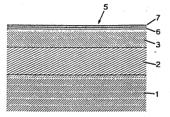
Referring to the succession of layers illustrated in Figure
2, materials and layer thicknesses identical to those
described with reference to Figure 1 are identified by the
same reference numerals. The succession of layers
illustrated in Figure 2 differs from that of Figure 1 only
by the fact that the contact layer 3 is covered by a double-
flash 2 instead of the surface layer 4 tFigure 1). The layer
6 of the double-flash 5, which faces the contact layer 3, is
a galvanically deposited PdAg layer with a palladium and
silver content of 50 % by weight each. The PdAg layer 6 has
a thickness of 0.1 ~m. It is covered by a galvanically
deposited surface layer 7 of a gold-cobalt alloy having a
thickness of likewise 0.1 ~m. Thus, the combined thickness
of the double-flash 5 is 0.2 ~m.
Hereafter, results obtained by frictional-wear measurements
will be described by reference to Figures 3 and 4. For the
purpose of determining the frictional wear, use was made of
brass parts in the form of wafers and in the form of spherical
caps of 3 mm radius. Both the wafers and the spherical caps
had the very succession of layers that was to be measured as
to its frictional-wear behavior. For purposes of these
measurements, the spherical caps were moved to and fro on
the wafers over a travel of 5 mm and at a frequency of
0.5 Hz until the coefficient of friction notably increased,
which indicates that irreversible, abrasive and/or adhesive
frictional wear has occurred.
The "coefficient of friction", measured as a function of the
friction cycles performed, is a measure of the friction
occurring when making or breaking an electric connection,
for example by means of a plug-in connection. It is the
- 8 - 21 07 6 9 6
result of the relation between the pushing and/or pulling
forces occurring during making and breaking of the plug-in
connection, and the contact pressure at which the two
contact layers are pressed into face-to-face contact. A
constantly low coefficient of friction is an indication of
low frictional wear.
In the case of the curve shown in Figure 3, the coefficient
of friction of the succession of layers described by
reference to Figure 1 was measured as a function of the
number of frictional cycles performed. The curve shows that
the coefficient of friction, starting at an initial value of
approximately 0.5, rises slightly after approximately 10
friction cycles performed, and then notably after
approximately 80 friction cycles, reaching values of over
0.6. This indicates that particles have formed between the
sliding surfaces, which then contribute to a rapidly in-
creasing frictional wear.
In the case of the curve shown in Figure 4, the coefficient
of friction of a contact element whose succession of layers
includes the double-flash, as illustrated in Figure 2, was
measured as a function of the number of frictional cycles
performed. The curve shows that the coefficient of friction,
starting at an initial value of approximately 0.3, remains
almost constant at a low level for more than 2000 friction
cycles and commences to rise only thereafter.
It is especially noted that the contact elements for which
the measuring results represented in Figures 3 and 4 were
obtained, differ only by the fact that in the case of the
prior-art contact element illustrated in Figure 3 the
surface layer consists of a gold layer of 0.2 ~m thickness,
while in the case of the contact element according to the
210769 6
invention, as illustrated in Figure 4, the surface layer is
a double-flash consisting of a PdAg layer of 0.1 ~m thick-
ness and a gold layer of 0.1 ~m thickness. The comparison of
the measuring results clearly shows the positive effect
which the PdAg layer, being only 0.1 ~m thick, has on the
frictional-wear behavior of the electric contact element
according to the invention.
Similar measuring results were also obtained for contact
elements with contact layers of palladium-nickel and silver-
tin alloys, and of nickel-phosphorus, covered by a double-
flash. It is to be expected that similar positive aspects of
the double-flash will be obtained also when applied in
combination with other contact layers.