Note: Descriptions are shown in the official language in which they were submitted.
-~ 2108~19
- l - Docket: 0618-26
i
RovFn FQUA~ ~7r~G A~P~ r
Field of ~hP InvPnti-~n
This ;nvention relates to eq~qli7~ e.~ and. in particular, to
such a~ ;el~ that are used to restore a subs~qntis1ly flat, for example,
overall frequency ,e~0ll3c with respect to signals that have been
l,a~ d through î~ u~n~;y de~n~le~l n~,twol~ incl~ ng ~are~;cC;~n
lines, etc.
R-~ 1 of thP InvPntion
Al~hough the present invention is h~.~t.. des~ d with respect to
video eq~s~ nE rmrlifiçrs for compensating losses qe50c~ 1 with coaxi. l
cable used by the profess;onql tele.;i,;on indu~hy, it is to be ul~d~ ood
that the invention can be applied to any situation involving the ~.~n~ ;on
of any type of signal over any type of Ç~,qucll.;y ~epe~e ~ n~,tw~J.L where
it is desired to restore a co~ ,t~d (typically flat) overall fle~luell~iy
.~onse.
Analogue TV signals are disl.;l.ut~,d in a system via coaxial cables.
Such cables have a signal loss cl,~.~ h . ;~I;c which is L~lu~ e~-depel.de .-.
with the loss at the higher video L~ u~ :es (e.g. S MHz) being much
greater than the loss at low r.~ s (e.g. below 100 K~). When the
length of such cables exceeds 30 feet, the effect of relatively greater
attenuation of the higher fre4~ .. rs may become objecti- - ~bl- because of
the loss of picture detail and color saturation. The loss of color occurs
. . ~ --
1 9
- 2 - Docket: 0618-26
because the NTSC color system employs the e ncod~ of color info.llldlion
onto a 3.58 MHz subcarrier (4.43 MHz in the PAL system) and saturation
is in propollion to mod~ tion ~...l l;l~.d~.
It is common practice to employ eql~qli7in~ ~mrlifiers to co,--~ nrht~,
for such cable losses. The adju~llllc.ll of such prior-art ~ ,a to match
a particular cable length is a co-~, '~~c procedule. It normally involves
several adj..sl~ ~e .l~, each of which apply primarily to a di~r~ ,nl part of the
rl~iquellC,y 9pCCI~ul~l but which typically interact. To aGcQ- .l~ h precise
eqll~li7~tion ~ uil~s the availability and use of fi~quc~lc~ sweep g~,ne.~.tola
and ~cso~ ed me~Curir~E cq~ I This pl~celul~i is further
complicated by the dict~nce b~ n the ends of the cable, which l~,pl~,se.ll
the ge.lc.ator and l..eas~;ng c~lu;l....e.~ loc~tione. In general, the
proce.lu,e is quite ~l;f icult and only the largest and best inet~ t;ons have
the ~. ce~C~ y e~u;r....~.~l to do this plope.ly.
An ~mrlifiPr which can eq~ i7ç a given fixed length of cable is
shown in Fig. 1. In this ~ , the eqU~li7ing nelwol~ 2 provides high
frequency slope adjusllllc.lt and co...r.;ces a comrle~ multi-section design
with a s~zlate adjuallllc.~l of the higher fre~,e~lr:es and perhaps
midfrequency adju~ t~i as well. The ~ S has a flat lei.~ol sc and
adjuak~le gain (the gain may be set to zero). The resultant correction
signal, which is oblained by al)pl~.;~t~,ly setting the gain of ~...pl;l;~.r 3,
is added to the incolllillg signal via ~ ...ng circuit 4 to provide an output
with co-rc~ d (flat) frequency l~i~onse.
At first, it may seem that, once the e~ A~ g n~,lw~l~ 2 is
calibrated, various lengths of cable may be nGco.. od.. ~ed by ay~opl;~t.,lysetting the variable gain ~mrlifier 3, but this is not so. Consider the case
where ~mrlifier 3 and n~,LwulL 2 have been calibrated for 500 feet of
cable. If the cable length is in.,l~ased to lQ00 feet, it might seem that if
-' 2108319
- 3 - Docket: 0618-26
the gain of ,mplifiP.r 3 were doubled, the cable co...i~n~-l;on would be
correct. In fact, the high-Çle~luellcy colu~llsation would not be suffini~P.nt
If, for example, for 500 feet of cable, the amount of 100 KHz signsl
passed is 95% snd the amount of l0 MHz signsl is 70%, then it follows
that for the 1000 feet cable, the output would at 100 KHz be 90.25% (.95
x .95) and at l0 MHz would be 49% (.7 x .7). Thus, as the cable length
is increased, the input to the filter n~,two,L 3 beco~ s defi~ P~lt in high
L~ en~:Ps; lhe~fo~e~ the filter shape must change in order to meet the
lsrger demand for high L~t~ucr~cy correction. Obviously, a COI1~ filter
,~spù~lse will not work for both cases. There is a cqe~ ~ effect which
lt~lUil'~,S a dirr~,ul equAAli7i~ ~ wulL for the longer cable. This is the
reason for the mllltirlP. adju~ ; in the prior-art ~...pl;l~
S~ of thP. InvP.ntir)ll
It is thus a ~;lllal y object of this invention to provide an equ~li7.ing
s~l-plirlcr which exhibits ~u~ ;-l improv~,l.e.l~ in ease of use and
accuracy of equ-Ali7~tion
It is a further object to provide such an ~ for use in the
eqU-li7A~tion of losses a~oc;-~t~,d with the coaxial cable used by the
profescionql television ill.lu~
It is a further object of this invention to provide a single-control
equ-Ali7er having a n~lwulL design~d to exhibit a colu~oullding effect versus
the amount of correction l~.luil.,d.
The Çol~ ~oing objects may be rl~m~.nted by an aul~ ing and
equAAli7.ing means in which the setting of only a single control is able to
co...~ c~le for the frequency~ep~.n.l~ ~ loss of the t.~n~...;cciQn cable.
A further object of this invention is to provide an improved
2108319
4- Docket: 0618-26
equAli7ing ~mrlifi~r wh~reill the correction of the cable loss at any one
rle.lue~ will cause the entire frequency l~s~n~nse to be flat, for example.
This is readily accomrlieh~ d without special test e4u;r....~ ~ (the sweep
~enerato,~ of the prior art, for e~A~ le) by feeding the cable with a correct
normal color signal and observing the ~mrlifiPr output at the cable
receiving end. For example, if the color burst ~I..pl;l~de (or some other
indi~Ptor of high frequency loss, for example) has been diminished by the
cable loss, the equAI;7çr can be ~ ~: sb~ to restore it. At this point, not
only will the signal be correct, but the L~iquen~iy lwponse over the entire
pecllunl will also be flat.
These and other objects will become a~p~e.ll after a reading of the
specifi~tion and claims taken together with the drawing.
Rrjef nescri~rtioll of thP. Ola~
Figure 1 is a block diagram an eq~ i7ing ~mrlifiPr which iil~ at~,s
problems ~eSociAtrd with prior art equ~li7p~rs~
Figure 2 is a block diaglalll of an illus~ative eq~sli7i~ amrlifip~r in
accoldance with the invention.
Figure 3 is a block diagram of a further illu~ àliYe eql.~1i7ing
amrlifier in accordance with the invention.
Figure 4 is a mr~ifi~d block diagram of the eq~lAli7ing ~mplifi~r of
Figure 3 i~rl~ g further ~.;uil.~ aeeo~ L~ ..illh
Figures SA and ~B, taken together, corS~ "~ a scl- - ~.A1;r di~.u,
of the cilcuilly of Figure 4.
~ " 2108319
Docket: 06l8-26
n~t~ii~ Descr~ption of F~ef~,..ed F....l~o~
of thP InvPntinl~
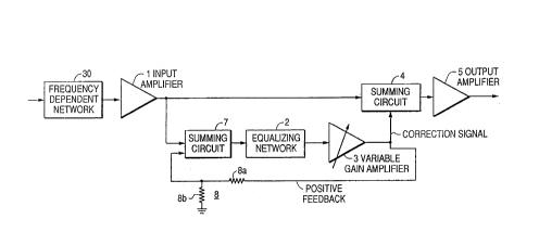
Referring to Figure 2, an eqi~q1i7ing ~mp1ifiPr in acco.~ance with a
first embodim~nt of the imention is illustrated wL~ in the input signal
from a frequency d~ndf, ~1 r.~,lwol~ 30 such as cable to be eqrq1i7ed is
applied to an input a ~p1;1~sr l. The output of the a~ sr is applied to
a su---~i~ circuit or node 4 in a first branch and a s.~ node 7 in a
second branch. The output of ~ e node 7 is applied to an e~ g
circuit means or n~twolL 2 where equalizing l..,lwol~ is frequency
depen~lP-n~ such that the i..,l~,..~ e thereof typically de~ ses with
in~ g f~ uclic~. The output of the e~ ;~ ~Iw~.L is applied to
a variable gain ~mr1ifiPr 3. The output of the v~;able gain ~mr1ifier is
applied to ~.~....i~ node 4 and, as positive C.e '~a-lr to ~ g node 7
via an ~ ~. B, CQ~ ;n~ pot-ntigl dividing .~;sl~.~ 8a and 8b,
where the employment of the positive f~ed~a-1~ is an iLIpolt~ll
chara~ g feature of the invendon. The correcdon signal applied to
s"....ni~e node 4 from the output of variable gain ~ 1;r;e~ 3 is ~ ed
with the output from n~p~ e~ 1 in ~ ng node 4, the output of the
....... ;~ node being applied to ~ p1;1;~.~ 5 which preferably has a flat
,ponse and adjustable gain where the gain may be set to zero.
In operation, as the gain of ~...p1;r;. ~ 3 is inc~ased, ~'iti~n~1 high
frequency energy is applied to n~lwol~ 2 due to the positive ~e~ll,a.~L
This results in a highfi~ ~n~;y boost at the input of n~p1;1~ 3, thus
effectively ~ g the shape of the lcsponse curve of r.~lwu.h 2. The
amount of a1~ ;on introduced by ~ tol 8 is such lo~ r with the
design of eq~ 7in~ n~lwulL 2 as to give a flat .~spoase for the type of
cable and range of cable length desired, for example, O ft. to lO00 ft. of
21 08319
- 6 - Docket: 0618-26
type 8281 (~mph~nnl, Inc.) cable. Too much a~t~....A1;on and there will
not be enough HF boost, too little and there will be excessive HF boost or
oscill~tion~
Hence, it can be seen that with the employment of the positive
~edl~c~ from the input of ~mplifiP~r 3 to sl.. il-~ node 7, a s~
in~p. o~e.llcnl in ease of use and accuracy of equ~li7Ation is achieved where
the equ~li7~t;oll can be simply effected by adjusting the gain of variable
gain ~mplifier 3 to thereby adjust the amount of positive feedbac~ this
a~ljus~n Pn~ being effected by a single control conn~ct~d either locally or
remotely to the variable gain AmplifiP,r.
Figure 3 is a block diagram of a further illu;~llalive e..,bo l; ...P ~-~ of
the invention ~ ;n the input signal from the cable is applied to Amrlifier
1 and the output of the ~...pl;l~P~r is applied to s, ...~ node 4 and
equ~li7~tiQn filter n~,lwolL 2. The output of equalization n~lwo.L 2 is
applied to the neg~Live terminal of an operational A...~ 3 having a
Ç~edl,~L resistor 10 also connected to the negative input thereof. The
output of the amrlifier 3 is co~ p~l~d to a potentiometer 11, the output of
the potentiorn~ter being connP!~;t~d to an A ll;fPr 9. The output of
A.n~l;r;P,~ 9 iS co.~ t~ as a correction signal to s ~ node 4 and as
a positive ~eJl~art signal to the positive input tenninal of Amrlifier 3 via
hi _ ~or 8. The output of the ~u.. ;n~ node 4 is applied to an ~mrlifier
5.
In operation, when potentiometpr 10 is set near ~in;~ .... output
very little energy is feed back to Amrlifi~r 3 Thus, the ~...p1;1~ fimctinn~
as a nonnal op-amp with gain at aparticular frequency prim~rily dep~ P.n~
on ratio of the value of resistor 10 to the value of the series i~ n~e of
n~lwol~ 2 wLer~y the gain of the op-amp incl~ases with increasil1g
frequency since the i.~ ed~ e of r~clwo-L 2 decl~ases with increasillg
2108319
7 Docket: 0618-26
frequency. When potentiometer 11 is set toward lllaX.illlUln output, the
feedback caused by resistor 10 causes the sarne signal to appear at the
negative terminal. This in turn causes the current through network 2 to
increase, especi~lly at higher fre4uel-c:es and thus the output of ~...pl;l;er
3 similarly incleascs. In essence, the filter n~,lwo,L 2 is being used twice,
once in response to the cable signal from ~mplifier 1 and once in lesponse
to the positive fc~ signal.
It should be noted with respect to the Figure 2 embo 1;,..f .~ that
filter n~,lw~lL 3 is also erR~ L~ly used twice, once in l~i~ol se ta the cable
~ signal and once in ,~sponse to the positive fee~har~ signal applied to
~u~ ..in,~ node 7.
As will be dese ;1 ed in further detail with respect to Figures 4 and
5A and SB, the equali7ir~ ~mrlifi~r of the present invention is preferably
remotely controlled ~lthough it is to be und~.alood that the equ~li7i~
amrlifier may also be locally controlled. It should be noted that remote
control of the equ~ tion run.,lion would not be prac~cal if more than one
frequency .~onse function were controlled. The ~rnrlifier is typically
used in co~ ec~ion with a remote l),~o~dcas~ truck (football, b~ce~?ll games,
etc.) to receive external signals over various lengths of cable (remote
Cd~ laS, feeds from other trucks, etc.) where every brc ad -~ct citU~tiOn wi]l
be dirrt.~ L. Hence, the easily adapted ~mrlifi~r in accollldllce with the
present invention is particularly adv~nt~ouc in that there is not time to
use e'-'~o,~e me~h~s to co~ Lly flatten the frequency l~ollse.
~ 2~ferring now to Figures 4, 5A and 5B, there is ill~ tcd in
further detail an equ~li7ing ~mplifi~r in acco~ ce with the present
invention where the CilCUi~ inf l~ es circuits conce,llled with sync
separation, video cl~...pil~ and remote control of gain and equ~li7~~ion
,~lthough some of the fo.~g~ing circuits are not required for the
.
210831~
- 8 - Docket: 0618-26
equ~li7~tion of signals in general, they will be generally described
he.~ ~. in col-n~cl;on with a ~ e~l,bodil-lent for the e~ on
of coaxial cable typically used by the professional television in-lu,l. ;es in
applications such as tho~e desçrihed above where for eY~rnrle the
amplifiers are used in connection with a remote broadcast truck. In
particular, the circuitry of Figs. 4, SA, and SB is de~i~n~d for use with
8182 (~mphçnol) type cable, the length of which may vary from 0 ft. to
1000 ft.
The following desc~irtion cim~ n~ously refers to both Figure 4 and
Figures SA and SB where the re1~tio~chir bel~ the c~ desc ;l-ed
hc.cinbefole with respect to Figure 3 are generally in~ir~tçd in Figures 4,
5A, and SB and are listed below togel]le. with equivalent el~..ç..l~; in
Figures 5A and SB. Moreover, in Figure 4 the ~u~ . l;ally equivalent
ek ..~ of Figures 3, SA and SB are generally in-lir~lt~o~l thereon.
FIG 3 FIGS. 5A ~n SR
Network 2 R76,52,61,78,79
CV2, C26,33,42,49
,~mplifilo.r 3 U6 (EL2030)
Pot 11, Amp 9 U7 (XT4122-20)
Remote Controlled ~mplifiçr
Su.. ;l-~ Node 4 R70,64 and U8
;r~. ~ S U8 (EL2030)
tor 10 R93 (below U6)
r 8 R100,101
The block diagram of Figure 4 in.tiratPs the i.~t~,.cn~ ction of the
3 1 ~
- 9 - Docket: 0618-26
main funrtion~l areas. Figure 4 may be referred to along with the
schem~tiC diagram of Figures SA and SB which provides further details
when read with the following desc~ ion.
Illl.;,LlaLve values of valious c~ are given in Figs. SA and
SB, it being understood these values are for pul~oses of illustration, there
being no intent to be limited to these values. Moreover, the elements U3;
U2; Ul; (U8, U6) (EL2030 ~ r~ ); US; U9; and U7 are co.l.l.lc~;ially
available from and l~s~cli~ly co.l~spond to Part Numbers 5Q0 103; 500-
020; 500-034; 500-102; S01-001; 501-023; and 504-064 of Ross Video
~imihCl, Iroquois, Ontario, Canada.
The video input signal is capacitively coupled to input stage emitter
followers Q3 and Q4 of input ~ 1. These feed â dirr~,.~,.~lial
a..~ er (Ql and Q2) which p~vides good rejection of commrln mode
hum. The push-pull signal from the coll~ctnrs of Q3 and Q4 is applied to
the inputs of U4, a remote controlled gain stage. UlB buffers the control
voltage for U4, as will be further ~es~ ed below. The push-pull outputs
of U4 are in current form and pl~luce small signals across R32 and R66.
These signals are amrlifi~d by Q7 and Q8 and drive emitter follower Q9.
The signal at the Q9 emitter should p.~Ç.,.~ly have its back porch
set to ground level for the a~pl;l~,~ circuits to function pro~.ly. To
achieve this, a sync sepalalo~ clamp pulse former and fee~baclr clamp are
used, the foregoing elernent~ being generally decign~ted at 16. The signal
from Q9 emitter is applied over line 17 and ~mrlified with a gain of about
5 and inverted by U5B. It is then coupled to pin 2 of USA, wbich
fun~ tion~ as a slicer as generally inr~ir~tf~d at 18 to sep~dte the sync. The
sync ~.aveÇc.l.,l appears at pin 6 of U5A. Cl, R35 and USD, as indicated
at 19, ~,ne~at~ a clamp pulse timed to sample the baclc porch. This pulse
turns ~mplifi~r U9 on, causing it to make a COIII~A~ ;COII between the signal
2108319
- lO- Docket: 0618-26
and ground level during the back porch. A correction signal is fed via Ql l
to Q7 of input amp1ifiçr l, thus stabilizing the back porch level.
The signal from Q9 of input ~".p1;~çr 1 also passes through
equA1i7Ation n~,lwolL 2 and then to ~IQ~p~ . U6, which cGlle~ponds to
~mp1ifi.or 3 of Fig. 3. As ~ cu~sed above, the output signal from U6 has
a frequency response characteristic desigr~d to replace the cable a~t~ n..~ion
of the video signal. In this regard, rer~;e.lce may also be made to U.S.
Patent No. 4,996,497 which is inCGl~o.,~te~ herein by lel;.,re~ce. The
output signal from U6 is applied to remote control gain stage U7, where
the correct amount of cable eq11~1i7-Ation may be set. As will be further
dcsc~;bed below, potentiQm~ter ll and ~ 9 of Fig. 3 are ~ nd
with mp1ifiçr U7 of Fig. SB and an equalization control signal is provided
via either local potpntiom~tel ~ or remote pot~ntiompte~ 21 (Fig. 4). A
portion of the output signal is pGi~ ly fed back via p l- ntiAl divider 8 to
the po~ , input of U6 as des~- i1 ed hc.~;nl~efo~c; to provide the requisite
eqU~li7Ation in acco~ance with the invention.
A further feature of the invention is that the setting of potentiom~ter
22 (or potentiomet~r 21) required to eqllAli7e a given leng~ of cable varies
S~.l9~ ;A11Y linearly with respect to the length of cable to be equalized
where with the potçntiom~ter set toward ..-;.-;...u--- output, the length of
cable is small. With the potentiom~t~r set at ~ output, lO00 feet
of cable is equ~1i7çd and with the potentiomet~ set half-way, sul.,~ y
500 feet of cable is eq lAli7çd, etc.
UlA stabilizes equAA1i7Ati~n control span by providing te.~ alul~
co...l~n~A~;on of U7 over the ~lO00 feet cable range. UlC buffers a
control .~iÇtl~ilce voltage which is ~ulL ;,IA..I;~A11Y equal to about ~e one-half
setting of potP.nt;omPtçr ~ (or 21). UlD buffers the control signal from
potentinm~r 21 (or 22). Potentiom~t~r RV6 sets the sensili~ily of the
~-" 210~3~
Docket: 0618-26
control signal applied from UID. Circuits U2 and U3 generally in~
at 20 in Fig. SB provide power regulation for the ~mrlifier.
The direct signal from Q9 of input ~mr1ifi~ r 1 and the equ~li7~til~n
correction signal from U7 are co.llbincd in output driving ~mrlifier U8,
which feeds six, for e~-a.l.i)le, outputs.
To further illustrate the co.l~,s~ dence between Fig. 3 and Figs. SA
and 5B, note the output from input ~mplifi~r 1 of Figure 3 occurs at point
A in Figure SA; the output of eq~li7~tinn n~,lwolL 2 occurs at point B; the
output of op-amp 3 occurs at point C; the output of remote controlled
~ pl;l~P~ U7 at point D; the output of attenuator 8 at point E; and the
output of summir~ node 4 and ~ 5 at point F. Thus, the video
signal oc~iu~ .;ng on line 12 of Fig. 5B, which is .~cei~,d from the cable to
be eq~qli7e~, is applied to emitter followers Q3 and Q4 of ~mplifier 1 as
in~ ted in Figure SA. The output of a~ ; ~ \ 1 oc~;u ~ e at point A is
applied to equ~li7~ti-.n n~,lwo~L generally in~ieqt~d at 2 in Figure 5A. The
output of the eqU~li7~ti~n n~.lwu.L oC~;u~;ng at point B is applied to the
negdliv~ input terminal of operational ~ pl;l~er 3 where the output of the
~n.l lir.cr is also applied to the negative input terminal via resistor 10. The
output of a...pl;l~" 3 is applied to remote controlled ~mplifier U7. A
portion of the output signal from ~mrlifier U7 is applied as positive
reeJb~ to the ~ositive terminal of ~mplifi~r 3 via the i.l~ O~
d~ n~ted at 8 and co...~ ing resistors 8a and 8b. Pct~ntiometer ~
provides local equ~li7~tisn control, the output of potPntir~mpter 22 being
applied through buffer UlD to ~mp1ifier U7 to control the amount of
positive fçedbac~ to ~mplifier 3. Remote control of the e4u~ ;on is
available from line 13 (Figs. 4 and 5B) and potenti~mPt~r 21 (Fig. 4) and
is also applied to ~...1~1;1;. ~ U7 via buffer UlD. A switch 38 is illu~ aled
in Fig. 4 to select the local or remote equqli7~tion although any hlown
~ ~1083~ 9
-12- Docket: 0618-26
means may be employed to effect this selPction The correction signal
obtained from ~e output of AmrlifiPr U7 is applied over line 14 to the
negative terminal of amrlifi~r S while the output from Amrlifiçr 1 is
applied to the positive terminal thereof via line lS.
Referring to Figure SA, addition-Al co..~ro~ CV3, R9S and CS0
are p.ere~ d to trim the .e.,~onse at longer cable lengths to thus effectively
remove what may be second-order effects.
It has been ac~u~ed throughout that the loss ~,h~..cte ;~I;c of all
s~. ~17s of a given type of cable are s~ffic;~ntly similar for a
pled~te.lllilled signal type and this in practice for ~lofc,s~:onql grades of
cable has been found to be the case.
Thus, in accol.ldllce with the present invention, an equqli7ing
a--~ er has been described whe~in the correction of cable loss at any
one frequency will cause the entire fi~luc.lcy ~9t~0n5e to be flat, for
~r? ~. In particul"r, with the Amrlifisr of Figs. SA and SB, a
su~alA ~ lly flat l~s~ollse from ~12 MHZ is obtaiAed. This is readily
a~comrliqh~d without special test e~ e~ by feeding the cable with a
correct normal color signal from a ler~..,.lc~ signal source 25 as in~i~qtP,~
in Fig. 3 where, for ~A~ le, the a...~ ,de of the back porch will be at
the correct level. (Note that if it is known that the ;...~p~ de of the back
porch, for çYAmp~, is not at the correct level as ~ ed from source
25, the gain of U4 (Fig. SA~ may be a~ .c~ed by a control signal applied
from line 30 via buffer 29 to thus set the back porch at the correct level.)
The output from ~mrlifie~ S at the cable l~.,eiving end can then be
obs~,. ved with a signal observation device 26 such as an osçilloscope where
the peak-to-peak voltage of the back porch can accordill~ly be observed.
Hence, for eY~mrle, if the color burst a...pl;~ ç (or some other indic~tor
of high frequency loss, (for ,~ ) has been dimit~;~h~d by the cable
~ ~108319
-13 - Docket: 0618-26
loss, the eq~ i7er ~an be ~ljust~ by a~ljust;ng the gain of ~ gain
amplifier 3 of Fig. 2 or ~ r U7 of Fig. 5A to restore the loss. At
this point, not only will the signal output at ~ . 5 be correct, but ~e
frequency l~,s~onse over the entire a~,llulll will also be flat.