Note: Descriptions are shown in the official language in which they were submitted.
CA 02108434 2002-11-25
i . _ . _
D-90-3-884 -1- PATENT APPLICATION
CAPACITIVELY COUPLED RF FLUORESCENT LAMP
WITH RF MAGNETIC ENHANCEMENT
~10~i~3~
-2- PATENT APPLICATION
FIELD QF THE INVENTION
This invention relates to fluorescent light
sources and, more particularly, to compact fluorescent
light sources wherein a fluorescent lamp is energized
by capacitively coupling RF electrical energy to a low
gressure discharge within the fluorescent lamp.
Improved operation is obtained by providing an RF
magnetic field in the region of the capacitive
coupling electrodes.
BACKGROUND OF THE INVENTION
Compact fluorescent lamps have been developed as
replacements for incandescent lamps because
fluorescent lamps are considerably more efficient and
have longer operating lives than incandescent lamps.
A compact fluorescent lamp has roughly the shape of an
incandescent lamp and can be installed in a
a0 conventional lamp socket. Prior art compact
fluorescent lamps have had one or more disadvantages.
A lamp ballast circuit is required, since fluorescent
lamps cannot be operated directly from line voltage.
The ballast circuit adds to the cost of the lamp and
ZS must be packaged in the base of the lamp.
Furthermore, the form factor of the fluorescent lamp
tube is less than ideal for use as an incandescent
lamp replacement because the light emitted per unit
volume is maximized in a long, small diameter
30 fluorescent lamp tube.
Current compact fluorescent lamps use a twin tube
or double twin tube architecture. Twin tube
1.i)~~3!1
-3- PATENT APPLICATION
fluorescent lamps typically include a pair of streight
tubes that are interconnected at or near one end to
form a generally U-shaped tube. Conventional twin
tube fluorescent lamps have filament cathodes at
opposite ends, and a continuous discharge extends
between the cathode filaments. A compact fluorescent
lamp using a frev_uency converting ballast to convert
60 Hz line voltage to a frequency in the range of 20-
30 kHz is disclosed in U.S. Patent No. 4,857,806
issued August 15, 1989 to Nilssen. The high frequency
output of the ballast is applied to the lamp
filaments.
Compact fluorescent lamps utilizing electrodeless
fluorescent lamps have been disclosed in the prior
art. A closed loop magnetic core transformer,
contained in a reentrant cavity in the lamp envelope,
induces a discharge in an electrodeless fluorescent
lamp in U.S. Patent No. 4,005,330 issued January 25,
1977 to Glascock et al. Discharge is induced by a
magnetic core coil within the envelope of an
electrodeless fluorescent lamp in the light source
disclosed in U.S. Patent No. 4,017,764 issued April
12, 197? to Anderson. In both of the above-mentioned
patents, the operating frequency is limited to about
Z5 50 kHz because of the lossy nature of magnetic
materials at high frequency. An electrodeless
fluorescent light source utilizing an air core coil
for inductive coupling at a frequency of about 4 MHz
is disclosed in U.S. Patent No. 4,010,400 fssued March
l, 1977 to Hollister. However, such a light source
has a tendency to radiate at the power of operation
and exhibits nonuniform plasma excitation.
~,10a~3~1
-4- PATENT APPLICATION
An electrodeless fluorescent light source,
utilizing frequencies in the 100 MHz to 300 GHz range,
is disclosed by Haugsjaa et al in U.S. Patent
4,189,661 issued February 19, 1980 High frequency
power, typically at 915 MHz, is coupled to an
ultraviolet producing low pressure discharge in a
phosphor coated electrodeless lamp which acts as a
termination within a termination fixture.
A compact fluorescent light source wherein high
frequency power is capacitively coupled to a low
pressure discharge is disclosed in U.S. Patent No.
4,266,167 issued May 5, 1981 to Proud et al. The lamp
envelope has an outer shape similar to that of an
incandescent lamp. An outer conductor, typically a
conductive mesh, is disposed on the outer surface of
the lamp envelope, and an inner conductor is disposed
in a reentrant cavity in the lamp envelope.
Frequencies in the range of 10 MHz to 10 GHz are
suggested. An electrodeless discharge tube wherein
high frequency energy is coupled to a discharge
through external electrodes is disclosed in U.S.
Patent No. 4,798,997 issued January 17, 1989 to Egami
et al. Another electrodeless fluorescent light source
which is energized by a high frequency power source is
disclosed in U.S. Patent No. 4,427,923 issued January
24, 1984 to Proud et al. In all of the lamps that
operate at high frequency, it is important to minimize
radiation of the high frequency energy.
It !s a general object of the present invention to
provide improved fluorescent light sources.
210~~:~%~
-5- PATENT APPLICATION
It is another object of the present invention to
provide a compact fluorescent lamp that is suitable
for replacement of an incandescent lamp.
It is a further object of the present invention to
provide a fluorescent light source wherein a
fluorescent lamp is capacitively driven by RF
electrical energy.
It is yet another object of the present invention
to provide an RF driven compact fluorescent lamp which
produces very little RF radiation.
It is another object of the present invention to
provide a highly efficient fluorescent light source
wherein a fluorescent lamp is capacitively driven by
RF electrical energy.
It is still another object of the present
invention to grovide fluorescent light sources which
are low in cost and easy to manufacture.
SUt~tARY OF THE INVENTION
According to the present invention, these and
other objects and advantages are achieved in a
fluorescent light source comprising a fluorescent lamp
having first and second electrodes disposed at or near
the ends thereof for capacitive coupling of RF
electrical energy to a low pressure discharge within
the fluorescent lamp, and tan RF source having a first
output lead electrically coupled to the first
electrode and a second output lead electrically
coupled to the second electrode. The electrodes
include means for inducing an RF magnetic field within
the fluorescent lamp near the electrodes. The RF
21U~~~3~
-6- PATENT APPLICATION
magnetic field locally increases the plasma density
and the sheath capacitance and reduces the RF voltage
across the fluorescent lamp and the sheath losses. As
a result, the RF magnetic field increases the
efficiency and the life expectancy of the fluorescent
light source.
The first and second electrodes can comprise
conductive coils wound on the outside surface of the
fluorescent lamp at or near the ends thereof for
inducing an axial magnetic field within the
fluorescent lamp. In a preferred embodiment, the
conductive coils comprise flat ribbon conductors on
the outside surface of the fluorescent lamp for
increased capacitive coupling. In another embodiment,
the first and second electrodes each comprise a
conductive layer on the outside surface of the
fluorescent lamp and a conductive coil disposed around
the conductive layer for inducing an axial magnetic
field within the fluorescent lamp. Each conductive
layer is preferably provided with an axial gap to
prevent circumferential current flow. In a preferred
embodiment, the conductive coils for magnetic
enhancement are part of a resonant tank circuit of the
RF source.
The fluorescent lamp can comprise a twin tube
fluorescent lamp having two straight tube sections and
an interconnection between the straight tube sections.
When a twin tube fluorescent lamp is used, the
magnetic field within the fluorescent lamp can be
increased by providing a ferromagnetic element between
the straight tube sections at one or both ends of the
t~~-~~~
-7- PATENT APPLICATION
conductive coils. Alternatively, the fluorescent lamp
can comprise a straight, tubular fluorescent lamp.
When necessary, the light source includes starting
means for initiating a low pressure discharge within
the fluorescent lamp. The RF source preferably
operates on a frequency range of about 3 MHz to 300
MHz and. most preferably operates in a frequency range
of about 10 MHz to 100 MHz.
In accordance with another feature of the
invention, the fluorescent light source includes a
lamp base for supporting the twin tube fluorescent
lamp. The RF source is mounted within the lamp base
such that the light source can be installed in a
conventional lamp socket.
BRIEF DESCRIPTION OF THE DRAWINGS
For a better understanding of the present
invention, together with other and further objects,
advantages and capabilities thereof, reference is made
to the accompanying drawings, which are incorporated
herein by reference and in which:
FIG. 1 is an elevational view of a twin tube
fluorescent light source that is capacitively driven
by RF electrical energy;
FIG. 2 is a schematic diagram of one example of an
RF source that is suitable for the fluorescent light
source;
FIG. 3 is a graph of fluorescent lamp discharge
power as a function of RF voltage;
FIG. 4 is a graph of relative light output as a
function of discharge power;
2108~3~
-8- PATENT APPLICATION
FIG. 5 is a partial schematic view of the twin
tube fluorescent lamp in the light source of FIG. 1,
showing external capacitive coupling electrodes and a
starting device;
FIG. 6 is a partial schematic view of an alternate
embodiment of the fluorescent light source, showing a
twin tube fluorescent lamp having cold cathode
electrodes and a high permittivity dielectric material
to enhance starting;
FIG. 7 is a schematic diagram of a twin tube
fluorescent lamp which utilizes RF magnetic
enhancement of capacitive coupling;
FIG. 8 is a schematic diagram of a twin tube
fluorescent lamp which utilizes RF magnetic
IS enhancement of capacitive coupling and includes
ferromagnetic material to increase the magnetic field
within the fluorescent lamp; and
FIG. 9 is a schematic diagram of a twin tube
fluorescent lamp which utilizes RF magnetic
enhancement of capacitive coupling and includes
conductive layers to increase electrode area.
DETAILED DESCRIPTION OF THE INVENTION
A fluorescent light source that is capacitively
driven by RF electrical energy is illustrated in FIG.
1. A twin tube fluorescent lamp 10 is driven by an RF
source 12. The RF source 12 is preferably mounted in
a base 14 of the light source. The base 14 supports
twin tube fluorescent lamp 10 and includes a plug 16
for installation in a conventional lamp socket. The
z~c~~~~3~~
-9- PATENT APPLICATION
RF source 12 is powered by conventional line voltage
received through plug 16.
In twin tube fluorescent lamp 10, a glass lamp
envelope contains a fill material, such as argon and
mercury, for sustaining a low gressure discharge and
has a phosphor coating on its inside surface. The
term "twin tube fluorescent lamp" is intended to
include any fluorescent lamp having two generally
straight tube sections that are interconnected at or
near one end. Examples include U-shaped lamp tubes as
shown in FIG. 1 and parallel tube sections that are
joined together by a "kiss joint".
The fluorescent lamp tube 10 has capacitive
coupling electrodes 20 and 22 at or near the ends
thereof for capacitive coupling of RF electrical
energy from source 12 to a low pressure discharge
within lamp 10. An output lead 24 of RF source 12 is
connected to electrode 20, and an output lead 26 is
connected to electrode 22. In the embodiment of FIG.
1, the electrodes 20 and 22 are formed on an external
surface of the lamp envelope. The low pressure
discharge within fluorescent lamp 10 emits radiation,
typically in the ultraviolet, which stimulates
emission of visible light by the phosphor coating.
Suitable phosphor coatings are well known in the art.
The RF source 12 preferably has an output
frequency in the range of about 3 MHz to 300 MHz.
Most preferably, the operating frequency is in the
range of about 10 MAz to 100 MHz. The use of RF
frequencies rather than microwave frequencies (1 GHz
or more) permits the fluorescent lamp 10 to be driven
with a relatively inexpensive, efficient and easily-
~, ~ ~ ~ ~' f ~~ ~J
-10- PATENT APPLICATION
built power source. The capacitive coupling technique
is advantageous over prior art inductive coupling
techniques because of its simple implementation and
its relatively high efficiency at low discharge power.
Unlike inductive coupling, the capacitive coupling
technique makes it possible to effectively energize a
twin tube or double twin tube fluorescent lamp.
In the lamp of FIG. 1, RF electrical energy is
applied to the external electrodes 20 and 22.
I0 Displacement current is coupled through the glass
envelope underlying each electrode, preferably with
sufficient RF voltage to initiate a low pressure
discharge. Plasma sheaths form on the insider of the
glass wall opposite the external electrodes.
Displacement current couples through the sheath that
forms between the charge neutral plasma body and the
wall, and conduction current is driven through the
plasma column. The resulting gas discharge column is
virtually identical to the discharge in a conventional
fluorescent light source. However, the plasma sheath
adjacent to the electrodes are quite different from a
conventional fluorescent lamp in that the sheaths form
a capacitor that acts as a ballast for the discharge
and limits the discharge current. In addition, ion
currents in the RF discharge are substantially lower
than found in a low frequency fluorescent discharge
lamp, thus resulting in less ion flux to the electrode
area.
A schematic diagram of a suitable RF source 12 is
shown in FIG. 2. A single field effect transistor 30
functions as an amplifier and an oscillator at a
frequency of 27.12 Irgiz. A bridge rectifier 32 and a
~' 1 i)->~.'~
-11- PATENT APPLICATION
capacitor 34 convert AC line voltage at 60 Hz to a DC
voltage. The transistor 30 operatos into a resonant
tank circuit, including an inductor 36 and a capacitor
3g, which provides sufficient starting and operating
. voltage on output leads 24 and 26 to initiate a
discharge within fluorescent lamp 10 instantly. The
output voltage is typically about 350 volts. The
disclosed circuit is low cost and simple to build and
uses a general purpose, commercially-available
transistor. The circuit produces about 8-12 watts of
RF power with an efficiency between 60% and 70%.
Since the transistor 30 operates with a grounded
drain, the drain can be attached to an available heat
sink. The lamp is driven symmetrically, thus reducing
ion flux to the electrode area and reducing RF
radiation.
Typical curves of the operating characteristics of
the fluorescent light source of the present invention
are shown in FIGS. 3 and 4. Discharge power as a
function of discharge voltage, with the fluorescent
lamp driven at 27 MHz, is represented by curve 50 in
FIG. 3. Relative light output as a function of
discharge power is represented by curve 52 in FIG. 4.
The operating characteristics in FIGS. 3 and 4
indicate that the fluorescent light source of the
invention is dimmable by reducing the RF voltage
applied to the twin tube fluorescent lamp. The lamp
can be operated from 3-10 watts with approximately the
same efficacy (lumens per watt) at all power levels.
The RF source circuit of FIG. 2 can be modified to
provide a variable RF voltage for dimming. As shown
in FIG. 3, the fluorescent lamp operates at about 350-
1 ii>S'~.i
-12- PATENT APPLICATION
400 volts, which corresponds to ~-10 watts in the
discharge. The overall output during normal operation
is estimated to be 50-60 lumens per watt. A preferred
operating frequency is 27.12 MHz because the FCC
allows radiation of significant power at this
frequency.
The twin tube fluorescent lamp used in the
fluorescent light source of the present invention
produces less RF radiation than a straight fluorescent
lamp because the twin tube fluorescent lamp as shown
in FIG. 1 is folded back on itself, thus limiting RF
radiation. Another advantage of the twin tube
fluorescent lamp configuration is that the coupling
ends are close together, thereby making it convenient
to attach the RF source without long leads and
possible radiation losses from coupling leads.
An enlarged view of one end of fluorescent lamp 10
is shown in FIG. 5. Electrodes 20 and 22 can be metal
layers, or bands, on the outside surface of twin tube
fluorescent lamp 10 at or near the ends thereof.
Because of the twin tube configuration, the electrodes
20 and 22 are adjacent to each other and are
relatively close together. Preferably, electrodes 20
and 22 have a relatively large surface area to enhance
capacitive coupling to the plasma of the low pressure
discharge within fluorescent lamp 10. In this
embodiment, no internal electrodes or filaments are
required within fluorescent lamp 10. At a frequency
of 27.12 MHz, external metal layers, or bands, 3/4
inch long are suitable for capacitive coupling of RF
electrical energy to the discharge.
:~ ( s I ;i 4 :, ;~
-13° PAT~HT APPLICATION
As noted above, the RF source 12 typically
provides an RF voltage of sufficient magnitude to
initiate a low pressure discharge within fluorescent
lamp 10. Although the RF voltage required to initiate
discharge depends on lamp construction, a typical RF
starting voltage is about 350 volts. In cases where
the RF voltage is not sufficient to reliably initiate
discharge, an additional starting device is preferably
utilized. An example of a simple starting circuit is
shown in FIG. 5. A notch 60 is formed in electrode
22, and a thin wire 62 is attached to the lamp
envelope in notch 60. The other end of the wire 62 is
connected to electrode 20. When the RF voltage of
source 12 is applied to electrodes 20 and 22, a high
field region is created within the lamp 10 adjacent to
notch 60, causing a discharge to be initiated. Since
the area of contact between wire 62 and fluorescent
lamp 10 in notch 60 is very small, the current flow is
very small and normal operation is not significantly
affected. When a discharge is initiated at one point
in the fluorescent lamp 10, the discharge then extends
through the length of the lamp between electrodes 20
and 22.
An alternative embodiment of the twin tube
fluorescent lamp suitable for use in a fluorescent
light source of the present invention is shown in FIG.
6. A twin tube fluorescent lamp 70 has internally
mounted cold cathode electrodes 72 and 74 at or near
opposite ends. The cold cathode electrodes 72 and 74
can be nickel or nickel impregnated with Hg (to
dispense Hg). To enhance starting, a high
permittivity dielectric fill material 76 is located
~.', i U ,e !~ ~ ~~
-19- PATENT APPLICATION
between the arms of the twin tube fluorescent lamp 70.
The high permittivity material increases the electric
field inside the tube in the volume between the
electrodes 72 and 74 sufficiently to initiate
breakdown. The high permittivity material can, for
example, be glass (Ey~S).
The performance of capacitively coupled RF driven
fluorescent light sources can be improved by creating
an auxiliary inductive RF discharge near the
capacitive coupling electrodes. The RF magnetic field
locally increases the plasma density and the sheath
capacitance and reduces the RF voltage across the
fluorescent lamp and the sheath losses. As a result,
the RF magnetic field increases the efficiency and the
life expectancy of the fluorescent light source.
Capacitively coupled RF driven fluorescent light
sources are efficient at discharge currents where
sheath losses are small. The sheath is the thin
region adjacent to each capacitive coupling electrode
where a plasma does not exist. Since sheath losses
are proportional to the product of the ion current at
the electrode and the average voltage across the
sheath, more efficient operation typically occurs at
lower currents. However, lower currents may not
produce a sufficient light output from the fluorescent
lamp. Because the discharge current is limited by the
impedance of the electrode sheaths, higher discharge
currents are obtained by increasing the RF voltage
across the sheath. With increasing RF sheath voltage,
the average voltage between the plasma and the
electrodes increases due to rectification effects, and
the sheath losses increase roughly as the square of
li
-15- PATENT APPLICATION
the discharge current. For high currents, the
discharge may no longer be an efficient light source
because ion losses may account for a large percentage
of the total discharge power dissipation. The ion
losses do not contribute to the generation of light.
Rlthough the RF magnetic enhancement technique
described below reduces sheath losses at all discharge
currents, its main value is at higher discharge
currents where sheath losses are important. In
general, the technique involves the application of an
RF magnetic field in the region of the fluorescent
lamp near the capacitive coupling electrodes. The
effect of the RF magnetic field is to increase the
electron density near the capacitive coupling
electrodes. The increased electron density results in
a decrease in capacitive reactance in the sheath and
ultimately leads to a lower voltage across the sheath
than occurs without RF magnetic enhancement (at a
given discharge current).
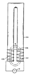
A schematic diagram of a twin tube fluorescent
lamp with RF magnetic enhancement is shown in FIG. 7.
Conductive coils 100 and 102 are wound around a twin
tube fluorescent lamp 104 near the ends thereof. Each
of coils 100 and 102 includes a few turns. The coils
100 and 102 are preferably wound as a single,
continuous conductor. In a preferred embodiment, the
coils 100 and 102 are the inductive element 36 (see
FIG. 2) of the resonant tank circuit in the RF source
12. This configuration saves space for the RF source
circuit, which is preferably mounted in the base of
the fluorescent light source as shown in FIG. 1 and
described above. The coils 100 and 102 are wound so
/.n ~.
-16- PATENT APP~.ICATION
as to reinforce each other's magnetic field and to
produce a generally axial magnetic field within
fluorescent lamp 104 near the ends thereof, as
indicated by magnetic field lines 106. The RF
potential on the coils 100 and 102 is capacitively
coupled through the glass ends of the twin tube
fluorescent lamp 104 and creates a capacitive RF
discharge that fills the twin tubs fluorescent lamp
104. To increase the capacitive coupling, the coils
100 and 102 may be formed as a flat conductive ribbon
wound on the ends of fluorescent lamp 104. In the
embodiment of FIG. 7, coils 100 and 102 perform the
functions of capacitive coupling of RF electrical
energy to the discharge within fluorescent lamp 104
and producing an RF magnetic field in the capacitive
coupling regions.
As the current flows through coils 100 and 102,
time varying magnetic flux is created in a direction
along the axis of each coil within the volume enclosed
by the coil. The time varying magnetic flux induces a
time varying electric field that drives an electric
current in a plane perpendicular to the axis of each
coil 100 and 102 and within the volume enclosed by the
coils. The induced current is opposite in direction
to the current in the coils 100 and 102. The induced
current enhances the electron density in the plasma
volume enclosed by the coils 100 and 102 and results
in a reduction in the capacitive reactance between the
plasma and the electrodes and ultimately results in a
reduction of sheath power loss.
A variation of the RF magnetic enhancement
technique is shown in FIG. 8. Like elements in FIGS.
~' LE) ~!1 ~~
-17- PATENT APPLICATION
7 and 8 have the same reference numerals. The
reluctance of the magnetic path at the ends of coils
100 and 102 is decreased by ferromagnetic elements 110
and 112. The ferromagnetic element 110 extends
between the ends of the straight tube sections of
fluorescent lamp 104, and ferromagnetic element 112
provides a magnetic Bath between ends of coils 100 and
102 at an intermediate region of the lamp 104. The
decreased reluctance increases the magnetic flux
within fluorescent lamp 104 for a given coil current.
The increased magnetic flux increases the induced
electric field, thus enhancing the effect for a given
coil current. It will be understood that either or
both of the ferromagnetic elements 110 and 112 can be
utilized.
A fluorescent lamp incosgorating RF magnetic
enhancement with an enlarged electrode area for
increased RF capacitive coupling is shown in FIG. 9.
Conductive layers 120 and 122 are disposed on the
outer surface of fluorescent lamp 104 at or near the
ends thereof. Each of the conductive layers 120 and
122 is provided with an axial gap 124 to prevent
circumferential current flow which wauld reduce the
magnetically induced electric field in the plasma.
The coils 100 and 102 surround conductive layers 120
and 122, respectively. Each coil is connected to the
conductive layer at the high voltage end of the coil
(at points 126 and 128). The coil should not touch
the conductive layer, except at one point so as to
avoid shorting of the coil turns. As indicated above,
the capacitive coupling electrode area can also be
increased by utilizing a flat ribbon coil. From FIGS.
'IV).~~~~1
-18- PATENT APPLICATE~ON
7-9 and the above description, it will be apparent the
capacitive coupling electrode and the RF magnetic
enhancement means can be separate elements as shown in
FIG. g or can be integrated into one element as shown
in FIG. 7.
The RF magnetic enhancement technique has been
shown and described in connection with a twin tube
fluorescent lamp. However, the RF magnetic
enhancement technique can also be applied to straight
fluorescent lamps and to double twin tube fluorescent
lamps.
While there have been shawn and described what are
at gresent considered the preferred embodiments of the
present invention, it will be obvious to those skilled
in the art that various changes and modifications may
be made therein without departing from the scoge of
the invention as defined by the appended claims.