Note: Descriptions are shown in the official language in which they were submitted.
~iO~1~3
BII)IRECTIONAL CLOCRING APPARATUS Wl'l'~l
AllTOMATIC SENSING
The lJ~e~&~ ~Lon r~lates generally to the field of
ele_Lo. ~c c.,~c~S rloc~in~
~mdo~beln~
lD .
A mi~.oc~o.- typically &~l~C~ an &~ al cloc~ to
operate. This clock can be sourced by a reference o~ lotor
that may have a h;gher frequency that is di~ided down to a
lower frequency for use by the microp.oce~, or other
15 ~.c uL ~ ~g a clock.
To reduce manufacturing costs, .li~t models of an
ele~onic dence can share the same pnDted circuit board
with only c~ components bedng chaneed. The .li~
nt~ may .cqu .~ e.c..t clock frequencie~ for y.~
~) operation. The di~r~.~t mo~l~el~ may also ~cqu rC the clock in
"t part~ of the circuit. The~e changes would ~qui~2
rhAngi~ the lcfer. .,ce o~llotA,r clock circl~it and the board
layout each time a di~.~t clock is needed. There i8 a
t;n~ need for an ap~ us that automot;cvlly senses the
~i clock and .li,e_ls a moAifie~l clock output to the appropriate
location ~lep~on~li~ on the clock's frequency and source.
S~gofthe ~ion
The &~IJ&La~u8 of the ~ ee,lt ~v_.Lion Pn~mr-o-~8e~ a
bidire~iAnol rlor~ing a~ Lus for 801~g and .~c¢;vh4;,
at di~re~ t times, a rlA~ir g signal on a single input/ou~ut
t~ aL The a~l,a.atus is co~.;sed of a clocl~ input
coupled to a ,efe-~. ce rlo~ ignol. Meon~ for CO!~
pulses of the ~ ce rlcrL ;.~ signal is co~ple l to the clock
input. The means for co~ has an overflow o~ to
,.
-2- 2 1 08493
indicate a count o~er~ow. A r~et input i~ coupled to a f~r~t
r~et sig~al that can be iD either a 1D~-1 igh state or a
logical low state. MP~n~ for ge~e.~ he first clo~
signal from the .~ 4e rlor~; .6 signal i~ coupled to the
5 clocl~ ~put. l~he mea~ for ge~e.al~, ha~ a~ output enohle
t~at ~o~trol~ an output tbat is coupled to the input/output
terminal. Means for gerw~al~ a eea~nd r~et ~i~al i~
coupled to means for ger~erating an enable signal. T'ne er ~hle
8~ i~ generated in re~pon~e to the o~erflow output, the
10 ~tate of the f~r~t re~et ~ignal, and the state of the ~ecQ~A re~et
~n~l The mean~ for pnc.~li~, the emable signal i~ coupled
to the output enable to co~trol the output of the means for
generating the rlQ~ 8~
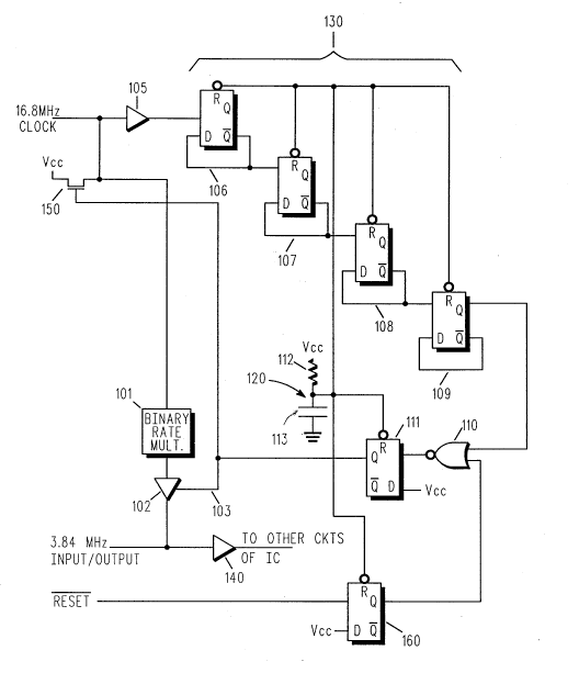
EIG. 1 ~hows a schematic of the ap~_~us of the
p.o~t i..~Lion.
~ IG. 2 shows a first blocl~ m of a mic.o~.o~30.
:i~ circuit usiIIg the bidir~;on-l rlor~ ap~a~u~ of the
.e~e~t ~e..tion.
~ IG. 3 shows a second blocl~ diagram of a
mic..up.oc~s~ circuit usi~g the bidire~ l clar~inp
a~alusofthep.ee~
EIG. 4 P,hOW8 a block diagram of a rad-oteJ~h~ in
accoLd&.ce with the l,.eee,lt iu~e~ n
rne bidire~iQn-l rlorL;.~ app~alus of t~e p.ee~ nt
~,e~Lon enables a single clock circuit to be used for multiple
AppliCA1;on~ where the clock source varies. I~e s~r~al,u~
senses the .efel~ce clock ~ource and frequency and
autoln~tir~lly ~ a modified clocl~ output to the
~ y~opriate circuit. This is accomplished u~g only one
-- bidir-ctio~al t~rmlnal of an $nt~grat~d circuit.
21 08493
-3-
l~ne bid~onal ~lnrL;~ a~a~u~ i8 illu~ated in
~lG. 1. In tbe ~.~f~.el ~m~iment, a .efe.~ce o~ator
generat~ a ~locl~ at a f~ of 16.8 M~ o ~ the
p~fer~d çm~liment~ a microproces~or and other ~
5 .~e a 3.84 M~z ~lo~ The 16.8 M~ ~ divided down
to the 3.84 M~z ~ by a binary rate mul~plier (lOl).
Tne binary rate multiplier i~ w~ll Icnown in the art as a cu~ut
that dindes a f~equen~r to an uneve~l multiple of the iDpUt.
Tne ou~put of the b~nary rate multiplier is eonnected to a
10 gate (102) han~g a }~ imp~d~n~9 cspability at tbe o~ t~
l~nis ~ impedanoe ~tate i~ controned by a oontrol ~put
(103). A logical high o~ the oo~trol input al~ows ~e ~ignal on
the input of the gate (102) to rea~ the output. A logical low on
the oontrol input ~ges the output of the gate (102) to a high
15 impe~Pnr,e.
An ac~ve pull-up device (160) ~th an ~;~e
impeA~nr~ of 101cQ at the 16.8 M~z ~loc} input is ~d to
.cl~ the e~ects of noise on the ~lo~ ~f5 ~1, The 16.8 MEz
~lo~ is also input to a ~ :' ( tri~er bu~er (105) to betteri~) define the edges of the ~lo~k ~ignal and to increa~e its noi~e
. Tne16.8MHz ~T-Plattheoutputofthebuffer
(105) is connected to the clo~c input of the first ~tage (106) of a
four bit counter. In the ~.ef,..ed çm~ o ~t,~ the co- ~t~-
(130) is made up of four D f~ip-flops (106 - 109) that areE; connected ~uch th~t the prior ~ta~e'~ inv-rting output Q of
the flip-flop~ i~ connected to the next ~e'~ clock input.
The non-~ I,illg out~ut of the Snal ~tage (109) of the
counter (130) iB rn e_~ to one of the inputs of a two input
NOR gate (110). The other input of the NOR gate (110) is
30 coD~ected, through a D flip-flop that allows only one reset
pul~e through, to a RESET signal that is generated from
another circuit. ThiB signal is used b~ other parts of an
el~Lumc dence that uses the bidireclional rl~L ;~lg
al,~at.ls of the pre~ent ~Lion. The RESET Isignal is active
3; low when power is applied to the cucuit of the ~.as~t
~4 210g~3
,..~Lon and c ., t ~lly rêaches a log~l high state after
al,l,.o~; ~t~ly 500 milli~cQ~Ids in the l,.efe,.~d emho~
l~ne output of the NOR gate (110) iB connected to the
clock input of a D flip - flop (111) that is used as a control latch
5 The D input of this flip - flop (111) i6 tied to Vcc This has the
effect of rlo~lri~ a lc~r~l high to the non~ ,- L;J~6 ouL~.Lt
when the signal at the clock input goes to a 1~1 low. The
Q~ l, of this flip-flop (111) is the control input (103) to the
three state gate.
lD A reset circuit (120), ~ of a resistor (112) in
series with a capacitor (113), 6~ ales a pre reset signal that
is connected to the reset inputs of each stage (106 - 109) of the
counter (130) and the reset input of the control lat~h (111). The
resistor (112) is tied to Vcc and the capacitor is tied to ground
In the ~,~fe,,~d eml~o l;~ t~ the resistor and capacitor are
chosen such that the c. ~; -I on 6 ~e~ate8 a pre reset ~ig~
that is low for app~o~im~tely 1 ms after power is applied to the
circuit, thus .~u ~ the co~ a to which this pre reset
signal is connected for the time that this signal is low.
The pre-reset Ei~n~l, the-efo.~, goes to a high state 499
ms before the RESET sig~al reaches the high state. This
c~ates a window of 499 _8 in which the control latch may be
rlor~e~l Once the RESET signal goe6 high, the output of the
NOR gate (110) will always be a logic low
The output of the three state gate is cnnnecte~l to an
input/o.~ S teL~i~al of the &y~&a~u8 of the l"es_.lt
..l io~ This té~ l is also conn~ to the input of
~nnt~er buffer (140) that lead6 to other ~l. uil~
When power is applied to the at.~..lus of the present
e~Lion, the pre-reset signal from the rêset circuit (120)
causes the outputs of the co t~ l (130) and the control latch
(111) to go low. The 16.8 MHz ~lock has no effect on the
o~ ~ te~ while the pre-reset sig~al is low. When the pre reset
signal goes high, the counter (130) starts col)nt;~ When the
36 counter (130) reaches 16, the output of the la~t stage (109) goes
low thus l~llQ;~ the o ~ ~ of the NOR gate to go high This
2~Q8~93
clocks a l~r~l high into the control latch (111). This high
control signal (103) enohb~ the three state buffer, allowing the
3.84 MHz si6~nal to reach the input/output tç~...;..~l as well as
the buffer (140) that leads to other ~ts. Thi6 also tliFohl?E
5 the pull-up device (150) to ,c~uce c~,~t drain.
If the 16.8 MHz clock is not ~a~c~t at the counter, the
control ~ignal (103) stays in the low state mo~ g the output of
~e three state buffer (102) a high ;~ --c~ This allows a
3.84 ~Iz clock that is g~J~.B~J in~ n~ nt of the
10 bidire~ ol clot,L ;~6 ~ B Bl,u8 of the l,.cce, t i~ lion to be
input at the input/output terminal and conducted to other
t~-,~18 by t~he bu~er (140).
It can be ~een i~om the above descnption that if the
electronic device using the bidirectional lo~ ;.~ tu8 of
15 the l~.eee~t iu~ Lion is gene.aLi~ a 16.8 MHz clock of its own
that must be divided down, the a~ tus ofthe ~e-~t
~Lon ~enses ~is and 6~,~e,stes a 3.84 MHz clock at the
input/output tenninal. This clock is then used by other
~, ub that are co ~P~te~ to the input/output te, ~ 1 as
well as ~. ,~ts ~nnQCte'l to the buffer (140). If the ele~L~vl.ic
device does not have a 16.8 MHz clock but Se-~l is
gene.~l.i~ its own 3.84 MHz clocl~, the &~a~ u8 of the
.e_~ "Lion senses this and allows the clock to be input
at the input/ou~l, terminal for use by other
connected to the buffer (140)
In the preferred emho~im~ont~ the bidirec~;on-o-l cloclrin~
ap~tus of the l~-e~e~t i~ Lion is constructed in a custom
~t~ ~..Led circuit. This mo-L-P~ the one t~- ;..~1 input/output
~.,Lu.~ even more desirable in that it only uses one pin of the
90 integrated circuit to provide either a clock output or to sccept a
clock input, ~lepen~linE on the fii~lot;n~l The &~ tuB of the
present invpn~ion~ tl~e~ru~, allows more pins of the
inteY~..ted circuit to be used for other uses
The bidirec1;~nol clorL ;.~ ap~ l u8 of the present
35 ill~lion is illustrated in FIGs. 2 and 3 in co~u~.,lion with
nol ~c~ FIG. 2 shows the a~a,al,us of the ~.ese..t
2 1 ~84~3
Lion in a ~lock output mode. The ,ere~e~ce osr~ tor
(201) inputs the clock signal to the il~te~st~ .i circ~ut (202)
havingthea~ usofthe~,ee.lti"~ ion. Theintegratet
circuit (202), through the bidirec~ nol clock pin, uuL~ul~ the
5 divided down clock to the clock input of the microprocessor
(203) and other ~,.,~uh ~ (204) n,e~ing the ~ A~ reA frequency
clocl~ The ~te~ ted circuit (202) may also contain a~ inn~
~ that ~equhe5 the divided down clo~ This iB
accomplished by routing the clock ;~te...~lly.
10~IG. 3 illu~ tes a clock input mode of the a~ .lus of
the ~.ec~t i~Lion. The clock that iB input to the
bidirectional ~lock pin of the integrated circl~it (202) having the
&~I,u8 of the ~ e~t i~ ..Lion is generated by the
mi~,ol,.oceseo,'s (303) crystal ~.uiL~ (304). This clock iB
15 used by the ad~li*~- Ql c~iL,~ in the ~t~,..ted circuit (202)
as well as other ~,vih~ (305) e 4-- ~l to the i~t~ l-ted
,uit.
While the bidire~;nn~l rlorL ;~6 ap~_l.u~ of the
e~lt il,vt:~hon can be used in any circuit, the ap~a~us of
the ~ ,ec~t il vt ,lhon is used in a radiotelephone in the
,lefe,,~d emho~lim ~nt~ A Q~mple block diagram of such a
device is illu~hated in FIG 4. The r-~lictel~lYh~ is
comprised of an _nt~nn~ (401) co~lp~e~ to a ~c~ - (402) and
Q~.;l lQr (403) tLo~;L a ~ ple--filter (404) The
otAleFhone i~ .olled by the mi~vl,.uc~seol (405) that iB
coupled to the integrated circuit (202) c~ .to;~ the
a~&latuB oft_e ~ e_.lt ~vr~ n The r~fel~,.lce oscill-tor
(201) inputs the ~lock signal to the ~te~l_ted circ~it (202)
The above ~QGC ;~ l UBeB 16.8 MHz and 3.84 l!~Iz as
30 clo~k freqllPn~efi Altern~tn emho-lim ~nt~ may use other
freqllPnrie~ ~Ppen~ e on the applis:s~t;on. The binary rate
mlll~iplier may also di-vide the input clock frequency to
another lequil~d frequenQ