Note: Descriptions are shown in the official language in which they were submitted.
210~fi73
~WO 92/18663 PCI /USg2/03133
METHOD AND APPARATUS FOR LINEAR MAGNETRON SPUTTERING
Description
Technical Field
This invention relates generally to the field of magnetron sputtering and more specifically tO
S linear magnetron apparatus for enhancing the uniformity of a plasma sheath along an elongated target
to provide a uniform sputtering rate along the length of the target and to provide a uniform thin film
coating on the substrate.
::
,
.~ .
.~
';~ ~:::
210g673
WO 92/18663 PCI`/US92/03133 ~'` `
,,
Background Art
Sputtering is a well-known process in which the surface of an objecl or substrate is coated
with a thin film of material that is sputtered, i.e., physically eroded by ion bombardment, from a
target. Sputtering is implemented by creating an electrical plasma over the surface of the target
S material in a low-pressure gas atmosphere. Gas ions from the plasma are accelerated by electric
fields to bombard and thereby eject atoms from the surface of the target material. These atoms travel
through the gas environment until they impact the surface of the object or substrate where they bond,
creating a coating layer. Sputtering has most commonly been used in the semiconductor industr~
where thin metal coatings are forrned on semiconductor substrates and then later patterned to form
10 the various conductive contacts, interconnections, and insulating surfaces on such substrates.
However, an ever-expanding variety of products are being coated by this sputtering process,
including, for example, architectural glass, computer screens, sheet steel, sunglasses, automobile
parts, automobile glàzing, surgical implants, jewelry, tool bits, sheet plastic, fabrics, and fiber optics.
Generally speaking, the articles to be coated have been of a flat or planar na~tre.
In a typical DC magnetron sputtering operation, a target of the material one wishes to use for
a coating is placed w thin a low pressure gas plasma and connected as a cathode. Ions from the gas.
most usually a chemically inert noble gas such as argon, bombard the surface of the target and knocl;
off atoms of the target material. The object being coated is typically placed with respect to the
cathode such that it is in the path of the sputtered atoms. Accordingly, a thin film of the material is
20 deposited on the surface of the object. It is the nature of the sputtering process that the sputtered
- atoms leave the target surface with relatively hir h energies and velocities such that when the atoms
bomhard the substrate surface they actually intermix into the atomic lattice of the substrate surf~ce.
creating a penetrating tight bond.
While the overall yield of the sputtering process, that is. the number of atoms sputtered per
25 incident ion, depends on the energy of the incident ions, the overall sputtering rate not only depends
on the energies of the incident ions, but also depends on the number of ions impacting the target
surface. The ion energy and number of ions are dependent on the level of ionization in the gas
plasma (glow discharge) and also upon the location of this plasma with respect to the target surface.
Therefore~ it is desirable that the ions in the plasma be produced adjacent the target surf~ce. so that
30 their energies are not dissipaled by collisions with intervening gas atoms.
A standard method of improving overall efficiency of glow discharge sputtering has heen t-l
:~ use magnetic fields to confine electrons to the glow region in the vicinitv of the cathode target
surface. The addition of such magnetic ftelds increases the rate of ionization. Numerous tvpes of
magnetron sputtering apparatus, as they have come to be known, have been developed for this ver
~lVO 92/18663 2 1 0 8 ~ 7 3 PCI`/US92/03133
purpose. Essentially, electrons emitted from the target surface will accelerate to a drift velocity tha~
is orthogonal tO both the directions of the electric field and the magnetic field as measured over the
surface of the target. In almost every magnetron sputtering device, the paths travelled t-y these
electrons close on themselves forming a closed loop. Further, the magnetic fields of such devices are
S typically designed such that arching lines of flux form "tunnels" through which the electrons travel
at drift velocity. lhat is, the electrons travel generally in "ring" or "racetrack" configuration: As
they rise from the target surface, the electrons whirl around the racetrack loop in proximity to the
target surface, thereby increasing sputtering rate, as discussed in the patents issued to Chapin, U.S.
No. 4,166,018; Class, U.S. No. 4,198,283; McLeod, U.S. Patent No. 3,956,093; and Corbani, U.S.
Patent No. 3,878,085.
In magnetron type sputtering devices, the efficiency of plasma generation is increased because
all of the electrons caught in the magnetic field have an increased effective path length in the
proximity of the target. That is, each electron emitted from the target surface has a much longer
distance of travel while in the pro~imity of the target. The result is that the electrons have collisions
IS with much higher numbers of gas atoms while near the target. Accordingly, the resultant higher
intensity plasma has more ions available to bombard the surface resulting in a higher spu~tering rate.
Another method of increasing the sputtering rate is described by Cuomo in U.S. Patent ~o
4,S88~490. Essentially, Cuomo adds an additional electrode, known as a hollow-arc cathode as ~
third and separately biased electrode to increase th~ numbers and energy of electrons generally
20 available in the vicinity of the target. However, a disadvantage associated with the addition of such
a hollow cathode is that the hollow cathode must be made of refractory metal because it operates at
extremely high temperatures. Another disadvantage associated with Cuomo`s hollow cathode is,that
it must be operated with a gas flow through the arc cathode that needs to be appropriately controlled
for proper operation. Yet another disadvantage is the need for an additional high-current b iasin~
25 supplv that must be set at an appropriate biasing level. In general~ Cuomo does achieve higher rates
because he is working in the right direction; higher rates are achieved by a "hotter" plasma mos~
proximale to the cathode surface. However, this increased sputtering rate comes at the expense ot`
a relatively large increase in the number of additional components and complex control apparatus~
Ma~netron sputtering systems can be classified into various groups. Principal among~ thes
30 groups are the circular, planar, and cylindrical types of sputtering apparatus~ Circular and r)lan;l:
mannetron apparatus tend to suffer from non-uniform erosion which renders the tar~et unusable e~ en
when relatively large amounts of useful target material still remain This nonunit`ormitv o1` erosi-~n
is a direct result of the "racetrack" effect described above. That is~ the plasma is more intense ovel
the racetrack area and sputters the target material directly below the racetrack at a vastly greater ral e
2108673
WO g2/18663 PCr~US92/03133 ,~
than the portions not directly below the racetrack. After this portion of the targct material is eroded
away, the target must be replaced even though material remains at the center and at the edges of th~
racetrack so that the device will not sustain damage to the supporting cooling structure. Since many
sputtering applications require expensive high purity target materials, this is an uneconomic and
5 wasteful circumstance. Actually, any of the current sputtering devices having a closed flux-tunnel
electron loop or racetrack configuration will suffer non-uniform target erosion, since the plasma
concentration necessarily varies over the surface of the target. Another disadvantage of circular and
planar magnetrons is that they tend to have quite bulky magnet structures making them large and
cumbersome. Because of this bulky structure, such magnetrons are generally useless for creating
10 uniform films inside concave or cylindrical structures.
Several different types of cylindrical magnetron sputtering devices have been developed in
~. .
part to solve the non-uniformity problems associated with the circular and planar devices, as described
above. Basically, the target material in a cylindrical device is in the form of an elongated tub~
Confining magnetic field.s are usually provided by complex bulky solenoid coils disposed within th~
15 target around the outside of the magnetron chamber as described in the patents issued to Penfold~
U.S. P;Qent~No. 3,884,793 and 4,031,424. Penfold uses solenoidal coils to generate magnetic fields
~having flux lines parallel to ~e axis of the dongated cathode target. Such cylindrical magnetrons tend
to be somewhat more even in their erosion patterns, however, they suffer from undesirable end
- effects. l~hat is, in a cylindrical magnetron the direction of the electron drift velocity vector causes
20 the electrons to orbit around a central target post. Unfortunately, however, the electrons tend to lea~;
out or escape their orbits near each end of the central post, resulting in lower ionization intensities.
thus lower sputtering rates, at each end of a cylindrical target. Further, such cylindrical magnelr~n~
are also expensive to construct and are not suitable for coating substrates with large planar surface
areas. Another disadvantage associated with the cylindrical magnetrons disclosed by Penfold is that
2~ the elongated target may not be bent or shaped to follow the contours of irregularly shaped objects.
If the target in a cylindrical magnetron, such as that described by Penfold, is bent or shaped to follo~
the contours of an irregularly shaped object, the magnetic field strength over the target surface ~-oll]~l
not be uniform, resulting in marked non-uniformities in the plasma sheath~ thus~ the sputterin(~ rat~
along and around the surface of the target. Further, because the magnetic field is axially oriented an 1
30 parallels the longitudinal axis of the elongated cathode of the target assembly, it is difficult~ i~` n~
impossible, to reshape the magnetic field so that it maintains the necessary uniform field strength over
the curved or bent target surface. Accordingly, such cylindrical sputtering devices utilizing axiall
oriented magnetic fields are not useful in uniformly coating irregularly shaped objects. McKelve!.
U.S. Paten~ No. 4,44~t997. realizes a fix for a somewhat non-planar surface. but his solution to th~
~V0 92/18663 2 t O ~ ~ 7 ~ PCI/US92/03133
s
problem is a device with multitudes of parts and a target surface that would be very expensive to form
with high-purity materials. Finally, a further disadvantage of these types of cylindrical sputtering
devices is that they are not useful for coating the inner surfaces of small diameter magnetic sleel
tubing, because the magnetic field produced by the solenoid outside of the tube cannot penetrate into
the internal regions of the tube.
T~he patent issued to Zega, U.S. Patent No. 4,376,02~, attempts to solve some of the
problems æsociated with the abovedescribed cylindrical magnetron sputtering apparatus by reorientin;,
the magnetic flux lines circularly around the axis of the elongated rod-like target material, as opposed
to the axial orientation used by Penfold. Essentially, Zega discloses a cylindrical magnetron device
utilizing a tubular currentcarrying electrode disposed within a tubular target cathode. Instead of using
a separate solenoid coil to generate the plæma-confining magnetic field, Zega uses a high-current
carrying hollow electrical conductor disposed within a tubular target to generate a circumferential
magnetic field that surrounds the tubular target. Zega presents data that show the device achieves
very poor uniformity of coatings. There is some improvement gained by the use of AC driving
potential for magnetic field generation, however, even depositions of coating are still not possible.
A fur~er disadvantage of ega's device is t'hat his cylindrical magnetron is still not useful for coating
large planar surfaces. Unlike the prior art magnetrons, the Zega magnetron, despite its poor
sputtering uniformity, does not depend on a closed-loop flux tunnel.
Corbani, U.S. Patent No. 3,878,085, did try to make a similar embodiment work t`or coatino
of planar surfaces. One of his patent embodiments shows a magnetron structure that is open-ended
with no looped magnetic field. He complains, however, that
nthe embodiment of Fig. 6 has the disadvantage that its path has a beginning an~d an
end, and that charged particles will be ejected from the end. Also, since there is a
beginning, sputtering will not occur for an initial length of the path~ and part of ~he
device is not functional for generation of sputtered material."
The disadvantage of Corbani's device is that it produces sputtering rates of different magnitudes
longitudinally along the surface. In operation, then, Corbani's de~ ice would gi~e a rate cur\ e simihtr
, to that shown in Fig. 2a of Zega's U.S. Patent No. 4,376~025.
In summary, none ofthese prior art DC magnetron sputtering devices are capable of achievin_
a uniform sputtering rate over the entire surface of an irregularly shaped target without going to great
pains and expense, such as in the device disclosed by McKelvey. There is a great need for an
inexpensive device that could be simply fashioned to coat such surfaces. Howe~er~ to do so would
ideallv require a target that is shaped to "silhouene" the okject so that the abiect heing coate(l can h;~
:
210867~
WO 92/18663 PCr/US92/03133,''~
brought adjacent the target in such a way that the distance between all points on the surface of the
object and the target are substantially equal. Unfortunately, prior art sputtering devices had to go to
extreme expense and complexity, sometimes sacrificing target use or power efficiency and almost
always introducing a large number of parts with a great surface areas into the vacuum system thus
S increasing the overall cost and comple~ity of the system~ Moreover, large surface areas and great
numbers of parts are antithetical to the creation of quality-high purity films in that they tend to poison
the sputtered film with unwanted impurities.
Furthermore, the aforementioned prior art devices tend to have relatively large targets of
much greater lengths or diarneters than would othenvise be necessary if such devices could achieve
10 a highly uniform plasma sheath over the target surface to provide at least an acceptable degree of
uniformity of the film deposited onto the substrate.
erefore~ there remains a need for a sputtering apparatus that is capable of uniformly and
efficiently depositing a thin film of the target material on objects having various shapes, such as the
inner surface of crucibles, the inner diameters of cylinders, shaped automobile glazing, and radjcall~
1~ curved lenses. Such an apparatus should achieve a uniform and intense plasma sheath evenl~ over
the full surface of the target to achieve umform erosion and high sputtering rates. Further such an
apparatus should have a target that can be easily placed in close proximity to the surface being coated
to increase the deposition efficiency and alleviate the problems caused by target atoms being sputtered
on objects in the vacuum system other than the substrate. Ideally, such a sputtering apparatus should
20 allow a wide variety of shapes, sizes, length, and widths of target cathode surface to be used while
maintaining uniform fluxes of sputtered atoms along the entire length of the target cathode surface.
Such a sputtering device should also be efficient, have a reasonable freedom from generating
contamination and particulates and still be relatively easy and inexpensive to manufacture~ Prior to
this invention, no such sputtering device existed~
~ - ~0 92/18663 2 ~ Q 8 6 7 3 PCI/US92/03133
Disclosure of Imention
Accordingly, it is a general object of this invention to provide a sputtering device tha~
achieves a uniform sputtering rate over the entire surface of the target.
It is another general object of this invention to provide a sputtering device capable o1
S depositing a very uniform coating on the surface of the object being coated.
It is a fur~er general object of this invention to provide a magnetron sputtering device
wherein the target can be conformed to a wide variety of shapes while maintaining a uniform plasma
sheath over the entire length of the irregularly shaped target.
lt is yet another general object of this invention to provide a magnetron spunering device tha~
- 10 can be used with equal effectiveness with AC or DC currents to create the confining magnetic field.
It is a specific object of this invention to provide a magnetron sputtering device that achieves
unif~orm deposition over planar surfaces.
It`is another specific object of this invention to provide a magnetron sputtering device having
a close fitting plasma sheath over a curved or bent elongated target to produce high spunering rates
15 with a high degree of uniformity over the entire length of the curved or bent elongated target.
It is a further specific object of this invention to provide a magnetron sputtering device that
achieves a uniform plasma sheath and uniform sputtering rate by using an electron emission enhan~ing
devlce.
It is yet a further specific object of this invention to provide a magnetron sputtering deviee
20 that can be used at very close working distances for achieving high spunering rates and target materi~l
uti!ization while mamtaining a uniform coating of sputtered target material on the object being coated .
It is another further specific object of this inven~ion to reduce the flux of emined splanered
large sized particles.
It is still another further specific object of this invention to provide a magnetron sputterin~
,
5 device that can be used to coat the ou~er surfaces of pipe, thread~ rod~ wires~ fiber optics~ and other
, , ,
., ~
elongated or tube llke materials.
210867~3
WO g2/18663 ` PCr/US92/03131'" ' "'
It is yet another specific object of this invention to provide a magnetron sputtering device that
can be used to sputter impurities from the inner surfaces of pipes or tubing having very small
~ diameters.
-~ Another specific object of thls invention is to provide a magnetron sputtering device that
S achieves high sputtering rates, even when used with magnetic materials.
Another object of this invention is to eliminate many of the parts and large surfaces that must
be contained within the vacuum sputtering chamber as well as to minimize the number of rotan~
- . ~
feedtbroughs and mechanical gearings that must pass through the vacuum chamber walls.
. .
`Additional objects, advantages, and novel features of the-invention shall be set forth in part
10 in thé descriplion that follows, and`in part will become apparent to those skilled in the art upon
examination of the following or may be learned by the practice of the invention. The objects and the
advantages of the invention may be realized ~nd attained by means of the instrumentalities and in
combinalions particularly pointed out in the appended claims.
- ~.
To achieve the foregoing and other objects and in accordance with the purpose of the present
Y;~ 15~; ~ invention, as embodied and broadly described herein, the emission enhanced linear magnetron
apparatus of this invention includes an elongated cathode surrounded by a target material. The tar, e!
material may either be a sleeve, or a wire wound around the elongated cathode, if the cathode is rod-
like, or the target material could be a welded sheet or a plate attached to or fastened around an
elongated cathode having another shape. Alternatively, and in either case, the cathode may be made
20 entirely of the target material. An electron emission enhancement device positioned near the front
, end of the elongated cathode enhances the emission of electrons by the cathode to create a hi~hl
uniform plasma sheath and sputtering rate along the entire length of the target material. A lo\~
voltage, high current AC or DC magnet supply connected across the elongated cathode generates a
plasma-confining magDetic field around~ the entire length of the cathode to further enhance efficienc~ .
25~ ~ If an AC magnet supply is used, an declron emission enhancement device must be positioned at each
end of the elongated cathode. In an alternate embodiment~ a single elon_ated tube of tarQet materi;tl
WO 92/18663 2 1 0 8 ~ 7 3 PCI`/US92/03133
can be conformed into a cathode, an electron emission enhancing device and a working end. The
working end can be formed into nearly any shape to conform to the shape of the surface being coated
with the target material.
The method of this invention includes the steps of providing an elongated cathode and target
S and an anode in a spunering chamber, enhancing the emission of electrons by the cathode, applying
an electric current through the elongated cathode to generate a coaxial magnetic field around the
~ ~ elongated cathode, and generating a tight, thin plasma sheath around the target.
:~.~' `
,
.
,, ~ .
~'
" ~ .
2108673
WO 92/18663 PCr/US92/03133 ~
Brief Description of the Drawin~s
The accompanying drawings, which are incorporated herein and form a part of the
specification illustrate preferred embodiments of the present invention, and together with the
description, serve to explain the principles of the invention. In the drawings:
S Figure 1 is a schematic elevational cross-sectional view of a first embodiment of a linear
magnetron sputtering apparatus according to the present invention showing the elongated rod-like
ca~hode, the coaxial hollow cathode electron enhaDca, the end terminator shell, and two trimming
anodes;
~ ~ .
. Figure 2 is a schematic elevation cross-section view of a target material coating cathode
: 10 having a cylindrical cross-section and showing how the magnetic field lines encircling the target
material confine the plasma adjacent the target material;
~; ~ Figure 3 is a schematic elevation cross-section view of a target material coating cathode
having a square or rectangular cross-section and showing how the magnetic field lines encircling the
target material confine the plasma adjacent the target material;
Figure 4 is a schematic elevational cross-sectional view of a second embodiment of a linear
magnetron sputtering apparatus according to the present invention showing the elongated rod-like
cathode~ the coaxial hollow cathode electron enhancer, and a single anode encircling the co'axial
: hollow cathode electron enhancer;
Figure 5 is a schematic elevational cross-sectional view of a third embodiment of a linear
20 magnetron sputtering apparatus according to the present invention showing the elongated rod-like
cathode, the coaxial hollow cathode electron enhancer, with a single anode disposed at the opposite
end of the sputtering chamber;
Figure 6 is a schematic elevational cross-sectional view of a four~h embodiment of a linear
magnetron sputtering apparatus according to the present invention, similar to the embodiment shown
25 in Figure 4~ but having an alternate flat plate electron enhancer connected to a separate electron
source power suppl~;
; "
- - ~wo g2/!8663 2 1 0 8 6 7 3 PCI /US92/03133
Il
Figure 7 is a schematic plan view of a special configuration cathode for coating laroe plan~r
surfaces having an integral coaxial hollow cathode electron enhancer;
Figure 8 is a schematic elevational cross-sectional view of a second embodiment of the special
configuration cathode shown in Pigure 7, but having a working portion curved to substantially follo~
5 the contour of the curved surface of the object being coated;
: Figure 9 is a perspective view of another special configuration cathode, wherein one end ot`
the elongated cathode is bent back on itself, forming a "U" section hollow cathode electron enhancer;
and
~: Figure 10 is a schematic elevational cross-sectional view of a fifth embodiment of a linear
10 magnetron sputtering apparatus according to the present invention, wherein the object being coated
: forms both the vacuum sputtering chamber and the anode.
': :
.
-~: -
-, ~
::
: ~ -
. ~
~108673
WO92/18663 PCr/US92/03133~`
12
Best Mode for Carrving OUt the Invention
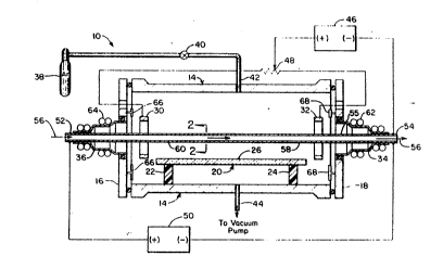
A linear magnetron sputtering apparatus 10 according to the present invention is shown in
Figure l and comprises an elongated, rod-like cathode 12 positioned axially in a vacuum chamber
defined by cylindrical wall 14 and opposite end walls 16, 18. A planar piece of glass 20 that is to
be coated is positioned on supports 22, 24 within the vacuum chamber adjacent cathode 12, so that
the surface 26 of glass substrate 20 can be coated with the sputtered metal. The source of the metal
material to be sputtered is the target 28, which can either be a sleeve or a- thick coating of the metal
material on the exterior surface of elongated cathode 12. Alternatively, target material 28 may t-e
a wire wound around cathode 12, or targa material 28 may be a welded sheet or plate-like surt`ace
connected to cathode 12. A pair of annular "*imming" anodes 30, 32 may be optionally positioned
ar~ound each end of cathode 12, to trim or finely adjust the density of the plasma sheath surrounding
the target 28, as will be described below. An electron emission enhancing device, such as coaxial
hollow cathode 34, is located at the "beginning" or front end 55 of cathode 12, also as will be full~
described below. An end terminator 36 is located at the opposite end of cathode 12. A suitable
sputtering gas, such as argon 38 is introduced into the vacuum chamber via valve 40 and inlet pipe
42. Suitable vacuum pump apparatus (not shown) connected to outlet pipe 44 maintains the pressure
within the sputtering chamber at a predetermined level.
In operation, the sputtering chamber is evacuated, and argon gas 38 is fed throucgh inlet r~ire
42 into the vacuum or sputtering chamber. A high voltage from sputtering power supplv 46 i~
connected eo cathode 12 and to both trimming anodes 30, 32~ via voltage divider 48~ as ~ill h~'
thoroughly described below. Alternatively however, as will become apparent below, trimming anodes
30, 32, may be discarded, and the outside wall 14 of the sputtering chamber may be used as th~
anode, or the object itself may be used as the anode, as will be shown and described belcw
However, for the purposes of continuing this description, it is assumed that the trimming anodes 30.
32 are used. This high voltage between cathode 12 and anodes 30~ 32 creates a glow discharge an~l
plasma in the argon gas adjacent the target surface 28 on cathode 12 forming a plasma sheath aroun-l
PcTlus92/o3 133
2 :1 0 8 ~ 7 .~ IP6~JS 2 3 JUi'~ 1993
13?~ -
target material 28. Essentially, electrons are discharged at hi8h energies from the cathode 12 into
the argon gas 38 to create the plasma in which the argon atoms are stripped of electrons and ionized.
These highly e~ccited ionized argon atoms from the plasma accelerate toward the cathode 12 and
bombard the target material 28 to sputter or erode atoms from the target 28. These sputtered atoms
S from target 28, also quite high in energy, migrate to the surface 26 of object 20, where they embed
and plate themselves onto the surface 26. Meanwhile, the spent, now low energy electrons from the
: ~ plasma migrate to the anodes 30, 32 to complete the plasma-generating electric circuit.
~: To enhance the sputtering efficiency aod to prevent tho high energy ions in the plasma from
~U :oth s~, includiog tho sur~ce 26 of objoct 20 beuu coatod, it is highly desirable to
10 confino tho glow dischargo and plasma sheath to tho aroa immediately surrounding the target matedal
28 on a~do 12. Such confin~t of tho glow dischargo al~t pl~ sheath u accomplishod by
~: ~ usmg c~hodo 12 as an dectric l oo~luaor to create a m~ic fidd in ~ion to the conventional
aod wdl-l~own use of the cathode 12 in sputtering a~ a polo and doclron sourco in tho high voltage
dectric fidd that creates the plasma Ihis additional or dual u~e of the cathodo 12 al~o as a low
: IS voltago, hi~h current conduclor to creato a ma~etic fidd that eocirde~ (circumferen~al ma~edc fidd
~ ~ B) tho c~hodo 12, ~d. con~equendy, target material 28 i~ uniquo at~ is an important feat~e
- of thia illv~tio~ To impla~t this dual fun~on of the cathodo 12 ~ both a hi~ ~roltago, h;8h
current coDductor tD cro tc conce~tric ma~netic fidd wi~ magnetic vecton B wr~ped
cir_ WUDt dlo ~thoto 12, t~o di~tinct ant ir~_ doctric circuit~ aro ooDn~d
20 to tho c~ 1~, ar ~ h Fi~urca 1, 4, S, and 6. lho co~~ rolta~o ~pu~
cirwit powcrod b~ olt~o pow ~upply 46 i5 co~nocted to tho c~odo 12 and anode~ 30, 32
as de~ed abovo. Iho add~o~l low ~olt~o, hi~h curt~t circ~ or cre~ tho uniq!lo
cira~ ~c field nctot~ B co~rially ~d tbo c~do 12 acco~ to thi~
invelltion ~ the low volt~o~ b c~t m~et power ~uwly SO co~octot t~ oppo~ite ~
2S of cal~do 12, which caue~ a ~ a~ to aOw ~y thrw~b c.lhodo 12. Ihi~ cu~ t aO
:
:~ a~iaty ~h cathode 12 i~ in ~ion t~, but fun~ioD~ inde~e~ly of, the conventional high
; '
U8STITUTE SHET
2108673 ~cr/us't~/031~3
P6~JS 23 J~:~l 1993
voltage sputtering circuit that was described above, and it creates the magnetic field with lines of
force or vectors B wrapping concentrically around the cathode 12 according to fundamental
electromagnetic principles and as illustrated in Figures 2 and 3. In the preferred embodiment, it is
preferred that the strength of the magnetic field generated around the target be at least about 250
S gauss as measured from a point about 1 mm above the surface of the target. As is well Icnown, the
dec~ic fidd E created by tho conventional hi8h voltage between an a~ode and the target/cathode
ac~g in combination with a magnetic field callses dectrons within the glow discharge created by the
high ~oltage circuit to gain a net ~docity, with the ma~itude and direction of the electron ~elocity
voctor beiDg ~ven by the vector cross product of the dectric fidd voctor E and the magnetic fidd
10 ~ector B. This dectron vdocit~ is also hlown as tho E X B ~docity. The predominate electron path
defines the portion of the target material that will be sputterod. The combination of unique concerltric
m~ic fidd ~vîth its fidd ~rocto~ B wr~d circumfereotially around cathode 12 and the
_high voltage doctric fidd E, is different than the low ~oltago, _ic fidd inducing,
axial flowing declric aurem in cathode 12, confines the high voltage ioduced, pla~generating
~15 dectron flow, (i.e. the E X B vdocity) to esse~ally a ~pirsl pattern with a slight radial component,
but mosdy an ~I compoDect, aroulld tho cathodo 12, thus confinin,~ tho glow dischargo and plasma
she~h to ~ iy ti~bt ~ ~I the target mate~ial 28. Finally, as wa~ b~iefly mendoned abo~le,
and as will be ~4bly de~ below, tho coa~cial hollo~ hode 34 loc~ted at tSe be_ or
~ont eot S5 OI c~ode 12, ~e~ lo enbance the emi!~sion of elec~ons at ~o cathode 12, rahiD~ Ihe
20 dectron dr~ a~t to a ~ed
,
~ 3!1aSTlTlii-~ S~ET
2108673
WO 92/18663 PCr/US92/03133
14
level such that it stays constant within the plasma sheath surrounding the surface of the cathode 12.
This saturated electron drift current results in uniform ion generation over the entire cathode 12~ thus
target material 28, thereby producing highly uniform sputtering rates of the target 28 regardless of
whether cathode 12 is curved or bent into irregular shapes, as will be completely described below.
S The primary advantage in using an electron emission enhancer, such as coaxial hollow cathode
34 in combination with the magnetic field that surrounds the cathode 12, is that highly uniform
sputtering rates can be easily achieved along the entire length of the cathode 12, even with a DC
magnetic fidd current. Further, since cathode 12 is used to generate the magnetic field~ cathode 12
can bo formd into a variety of shapes to provide close sputtering coupling, thus high deposition
10 efficiency, with irregularly shaped planar objects, without affecting the uniform and tight plasma
sheath surrounding the cathode. That is, the plasma sheath substantially follows any bends or curves
in cathodo 12. Finally, it is important to note that the linear magnetron sputtering apparatus
according to this invention does not require a closed loop field to achieve uniform sputtering at high
~ ~ ~ rates. For oxample, an elongated cathode loop, such as the one shown in Figure 7, can be easily used
- ~ ~ IS to coat the inside surface of a blind-end pipe, as will be described in detail below.
eferring again to Figure 1, with occasional reference to Figures 2 and 3. the linear
magnetron sputtering apparatus 10 according to the present invention is described in detail. As was
briefly described above, the sputtering target 28 is integral with cathode 12. so that the target 28
follows any bends or contours in the cathode. Target 28 may be either a sleeve or a thick coatin_
-~ 20 of the metal material on the exterior surface of the cathode 12. Alternatively, cathode 12 may
entirely comprise target material 12. For example~ if the target material 28 is copper, cathode 12
may simply be a length of copper tubing. Finally, water, or some other liquid or gas coolant may
be optionally introduced through open end 52 of cathode 12, flowing through the cathode and out
through exit end 54, in the direction of arrows S6.~ See Figure 1.
~; 2~ As wæ briefly described above, magnet current from magnet power supply 50 flows axially
down cathode 12 and creates a magnetic field having flux lines 41 that subs~antially encircle cathode
2108G73 J'~ S~/ (J3 133
JS ~ ', JlJN l99~
~ .
12 and target 28, as is best seen in Figure 2. Note that the magnetic flux lines 41 shown in Figure
2 would encirde the cathode/target in the opposite direction, i.e., in the clockwise direction, if the
low voltage magnet current from low voltage power supply 50 was flowing through the cathode 12
was reversed, as would be obvious to persons having ordinary skill in this art. Therefore, the linear
S ma~etron according to the present invention should not be regarded as being limited to any particular
field direct,ion, so long as the magnetic field vectors B are oriented circumferentially around, not
paralld to, the cathode/target. Note also that the cathode and target may be of almost any desired
cross soction. For e~campb, the cross section of the ca~ode 12 and target 28 may be sq!lare or
r~ular, and the flm lines 41 of tho _ic field will substantially conform to that cross-sectioD,
10 as shown in Fig~re 3. If a DC m~et current supply is used, the negative pole or terminal of
m~ pow suppb SO is connectod to cathode 12 at end S4, with the positive tenninal be~
con~ed bO end S2. With thu polarity, end S4 of cathode 12 is dle beginning end, and coa~cial
hoUow calhode 34 then f~m~ioD~ ~ the electron enhancer. FinaUy, cathode 12 is also coDnected to
the neg~ro te~minal of high voltage sputtering supply 46 atld the positive terminal of high voltage
sp~ing supply u connected to a~odes 30 and 32 via voltage divider 48. Wilh both supplia 46 and
SO en~d a~d with an argon pre~ure of about S~ torr, an inten~e glow di~c~arge and plasrna
~he~th forn~ cvenly ov thc dongated target 28.
~n opcr~on. a vy l~rg~~ emission of electrons is created over the ~iron~ e~d por~on SS of
target msti~l 28 tbat is ~ by ~ial hoUow cathodo 34, ~ is also in physical aod
20 decb~ a~t ~ c~odo 12. Thereote, the front e~d por~ SS of ca~hode 12 form~ ~e inner
doc~ of co~l ~aUow cU~dc 3~. Accordingly, hollow cathodo 3~ ~ve~ a~ a ~ource of
elec~ and photon~ to enb nco tho emusioD of electron~ at tho firo~ end portion SS of targe~ 28.
This e~ eloc~on e~b~t at tho front ~d SS of cathodo 12 ioctos~er tho elec~on driR cu~t
to ~, ~ ~t tho d~ cum~t r_ const~t withhl tho pl~ma sho~h over the sur~
- ~ ~ 2S of t~ot m~ 28. 11~ oth WotdS, thc current in the pl~ she~th is nised to ~ high eDough
u~c to e~bli~ ~ limitiDg, i.o., CoDStan[, curre~t in the plasm~ shalh. Only when this limi~n~
.
: ` SU8STl~u ~ L $~ET
2~ 867 ~S23JUNl9~3
condition is ach,eved is it possible to produce a plasma sheath having uniform thicl~ness and density,
thus establishing a uniform sputtering rate along the entire length of the target material 28.
In practice, it has been found that a si~c (6) inch length of the coa~cial hollow cathode 34 is
sufflcient wbere both tho target material 28 and hollow cathode 34 are copper and where the
S sputtering gas is argon. Howover, the emissiviq of the target matorial 28 depellds on tho particular
target msterial, sur&cc impurities, gas pressura, aod the partial preuure~ of any reactive gasses
~; ~ SUBSTlTUTc S~ET
:~ .
r~ 7~/ u~ 1S3
2108fi73 ~A~S 23 JUN l993
~w
present in the sputtering chamber. Therefore, it may be necessary to adjust the length of the hollow
cathode 34 to achieve a uniform plasma sheath. Alternatively, a solenoid or coil of wire (not shown)
can be wound around hol10w cathode 34 to stimulate the emission of even more electrons. That is,
increasing the current in such a solenoid will increase the electron emission of the cathode 12 until
S the sputtering rate is again equal at all points, such as points S8 and 60, along target material 28.
Therefore, for the purposes of this invention, a hollow cathode electron emission enhancer
may be considered to be any portion of the cathodeltarga material, or any other suitable material,
either at the cathode dectrical potential, or somo other electrical potential, that is positioned a radially
spacod di~ce from the be~inning end of the cathode so that it presents an opposed surface area that
10 is at lea~t par~ally e~cposed in radial relation to the beginni~ end of the cathode/target. Numerous
different oonfi~ions of hollow cathoda according to the present inven~ion aod consistent witll the
foregoiDg te~itioo, are. therefore, possible. By way of e~ample and as will be e~plained in greater
delail bdow" hollow cathode may comprise a hollow cylindrical ~shell~ (Pigure~ 1, 4, 5, aod 10),
a plate positib~ed a spaced distance f~om tho boginning end of the cathode ~igure 6), a portion of
IS the dongatod cathodo itself that is coilod around tho begin~4 eod of tho cathodo ~Figura 7 aod 8),
or a portion of a flat, bar-lilco cathodo that is bent baclc upon itself(Figure 9).
Ah~ooudy, the rdativo ~U rato at any point aloDg ths targe~ 28 can bo optictlly
~d dunng tho ~ o~on by me~in~ the ~hich~ of the pla~ma ~heath o~sr the
~o of t~t 28. For ~plo, sn ap~c~l micrometer telesoope ~ystem can bo used to det~ine
20 tho pluma~ thich~ ~t any point along tho target 28. If any diffasnco i~ det~d, tho rent
.... .
in tho op~ oleaoid wound around hollow cathodo 34 can bo adjusted ~ d~cr~ed above to
a~ bievo a uniform pl~ sheath. Alter~ rdy, a voltage divider 48 connected to tr~ing anode~
30 ~d 32 c~ bo adju~od to chlue du ~ive pote~l~ betwoen the t~ nodes 30 and 32
21 OD ~dy adjust tho pl~ ~, thw _bg rate. In ~ome iD~ es, the
2S da~ emusion ~d wi~h hoUow cathode 34, as wdl aa the doctron ~orption by end
ter_r 36 will eacces~h~dy heat these compoo~, noce~itating the addition of cooling coil~ 62
~ ~ ~ SUBST~ S~EET
21~673 ~C17US?~/03 133-
411S 2~3 JlJ~I 199~
and 64 surrounding co~ial hollow cathode 34 and end terminator 36, respectively.
FinaUy, in this embodiment, it is preferred that the end walls 16, 18 be non-conductive, so
that the cathode 12 may be run at a different potential from the walls 14 of the sputtering chamber,
which chamber is usually grourlded for safety. Therefore, annular sputter shields 66, 68 are placed
S circumferentiaUy around hollow cathode 34 and end terminator 36 to insure that a conductive
sputtered film doe~ not form a continuous conductive path between the hollow cathode 34 or end
terminator 36 aod walls 14.
~ advant4e of the magnetron sputtering device 10 shown in Figure 1 is that it can be
used with eilher a DC _t power supply, as was described above, or with an AC supply. If an
~ : 10 - AC mag~ qply is usod, the coa~cial hoUow cathode 34 and end termin~r 36 will alteroate their
fanc~. 1~ is, during ~ fint h lf of Ihe AC c~rclo, sbdl 34 might b Ihe eDd t~mi~r whik
; ~ ,
SUBSTITU,E S~ET
- ~VO92/18663 ~ 1 0 8 6 7 ~ PCl/US92/03133
shell 36 is the emission enhancer, and vice versa. Therefore, the apparatus 10 according to the
present invention is readily adaptable for either AC or DC operation, without the need to change or
replace any components. Finally, this magnetron sputtering device 10 permits the deposilion of
ferromagnetic target mate~ials at a rate approximately equivalent to that achievable with non-
S ferromagnetic conductive target materials.
A second embodiment 110 of a !inear magnetron sputtering device for DC operation only isshowo in Figure 4 being used to coat the inside surface of a cylindrical object. Essentia
lly, the
cadlode 112 coated with target material 128 is positioned in a sputtering chamher defined h~
cylindrical wall 114 and opposite end walls 116 and 118, just like the first embodiment 10. The
cylindrical object 120 is positloned in the sputtering chamber concentrically around the cathode 112
so that the inside surface 126 of the substrate 120 can be coated with the target material 128. In this
second embodiment, however, a single annular anode 130 surrounds coaxial hollow cathode 134.
Argon gas 138 is introduced into the sputtering chamber ~rough coaxial hollow cathode 134. An
end shield 166 is positioned around the opposite end of cathode 112 to protect the ad jacent end wall
118 &om sputtering damage. The operation of this second embodiment 110 is essentially identical
:` ~ tO the first, except that only DC magdetic field currents can be placed on cathode 112~ because there
is not an opposing end terminator that can function as a coaxial hollow cathode for the half of the~ AC
cycle having reversed polarities. ~
A third embodiment 210 of a linear magnetron sputtering device, a ain t`or DC operation
20 only, is shown in Figure 5. Essentially, this third embodiment 210 is the same as the second
embodiment 110, except that the anode 230 is located at the opposite end of the sputterin_ chamb~r.
When this anode 230 is relocated, as in this embodiment 210, the positive terminal of magnet su~pl~
250 should be connected to the end of the cathode 212 containing the coaxial hollow cathode 2'~
As with the second embodiment 110, this third embodiment 210 can on be operated with a DC
25 magnet current.
.
, ~,
WO 92/18663 2 1 0 8 ~ 7 3 PCr/US~2/03133 ~ `
18
A fourth embodiment 310 of yet another DC linear magnetron sputtering device is shown in
Figure 6. This fourth embodiment 310 uses a different type of electron emission enhancer to provide
electron enhancement in the plasma. This plate type of emission enhancer 335 is essentially a fla~
plate that is connected to an additional electron source power supply 351.
S While the above-described embodiments have all been shown and described utilizing straight,
rod-like targets, a nearly infinite variety of target shapes are possible, since the plasma sheath will
closely follow any contours, bends, or curves of the elongated target. The target can even be folded
back on itself to form a loop. For example. a special configuration 410 of a combination cathode and
~; target 412 loop according to the present invention is shown in Figure 7. This configuration of the
combination cat ode and target 412 would be useful in coating large, planar surfaces, such as large
glass plates. The plate 420 could be passed under or over the working portion 413 of combination
cathode/urga 412 in a direction parallel to the plane of the paper as indica.ed by arrow 443. The
elongated working portion 413 can be of any length, and preferably would be as long as the object
being coated. Since the object can easily be drawn past working end 413 in close proximity.
lS deposition efficiency will be relatively high, with the majority of the spunered target atoms coating
the surface of the planar object. Thus, a uniform coating on the surface of such a planar objec~ can
~be easi!y achieved on a single pass. The rate at which the object is moved past working portion ~1 "
controls the thickness of the plated material. Alternatively, this embodiment 410 -could be used to
coat the inside surface of a blind-end tube or cylinder, since the working portion 413 can be easil~
inserted into the open end of the cylinder and does not require a opening in the blind end to complete
the circuit.
, .
Referring now in detail to Figure 7, the combination catbode and target 412 is rnade from
tube stock of the target material, e.g., aluminum, gold, copper, etc. End plate 416 supports the
cathodeltarget 412 and mounts to some suitable vacuum sputtering chamber (not shown) large enou~h
to accommodate the object 420 being coated. In this special configuration 410~ the front end 455 of
combination cathode target 412 is necessarily the end that enters the sputtering chamber through
~0 92/18663 2 1 0 8 6 7 3 PCI`/US92/03133
19
insulating feedthroughs 413. Also, the generation of the magnetic field is necessarily done with direct
current from a suitable magnet power supply (not shown). Connecter 454 is connected to the negative
pole or terminal of the magnet power supply and connecter 452 is connected to the positive terminal
- of the supply. A suitable coolant can be directed through the tubing as indicated by arrows 456. An
S important feature of this special configuration 410 is that the plurality of coils 434 form the hollow
cathode emission enhancer around the beginning portion 455 of cathode/target 412, thereb~
eliminating the need for a separate element, thus reducing cost. The "working" portion or loop 413
of cathode 412 extends into the sputtering chamber in 2 straight line, which is preferred when coating
large planar surfaces. The individual tubes 411, 415 comprising working loop 413 should be
separated by at least three (3) or four (4) diamets of the tube stock comprising cathode 412, (shown
by arrow 441), so that the magnetic field compression and hollow cathode effects will not cause the
facing surfaces of these tube portions 411, 415 to be the only parts to sputter. However, there are
~` certain instances where it might be desired to sputter the facing surfaces of the tube portions such
as, for example, when plating both sides of a thin obJect passing between the loops 41 1. ~IS in
lS direction perpendicular to the plane of the drawing shown in Figure 7.
An alternative embodiment S10 to the special embodiment 410 is shown in Figure ~
- Essentially, this embodiment 510 is identical to the embodiment 410 as described above, exceptthat
this embodiment S10 has a curved or bent working portion S13 of combination target/cathode 51'
The working portion 513 is curved to substantially follow the curved contour of a curved class r~late
20 being passed adjacent working portion 513 perpendicular to the plane of the drawin~. The unit`orm
distance between the working portion 513 of the target and the surface 526 of the objec~ 520 hein~
coated allows a uniform coating to be applied with a high deposition efficiency.
It is important to remember that the sputtering target/cathode used in conjunction with the
principles of this invention can take numerous forms other than the forms shown and descrihed aho~e
2~ for the embodiments 410 and S10. For example, another possible configuration 610 of a sputterin
targettcathode 612 is shown in Figure 9. In ~his embodiment 610 the cross section ot` tar. et/catho:l~
2108573
WO 92/18663 PCr/US92/0313~ ` `
512 is rectangular, as opposed to cylindrical, as was shown for embodiments 410 and 510. nor do~s
the target/cathode 612 double back on itself to form a wand or loop, although it could if the pil e
being coated has a blind end, as described above. Such a configuration 610 for the target/cathode
would be useful when coating the inside surfaco of an elongated object, such as a pipe or gun barreh
as the entire cathode 612 can be appropriately sized to fit inside the object being coated. If such a
cathode 612 is to be used for DC operation, the hollow cathode emission enhancer 634 need only be
placed at the beginning end of the working portion 613 of the cathode 612 and can be formed h~
bending end 627 of cathode 612 back upon itself, as seen in Figure 9. If the cathode 612 is to be
used for A~ operation, a similar hollow cathode emission enhancer could be formed by bending end
629 back upon itself in a "U", similar to end 627. Note that only the target/cathode 612 is shown
in Figure 9. and suitablc electrical connections? voltage and current sources, and a suitahle sputterino
chamber would have to be accommodated similar to those shown and described above for the other
embodiments.
Still other configurations for the linear magnetron sputtering apparatus accordio, to the
present invention are possible. For example, for the embodiment 710 shown in Figure 10 is ideal
t-
for coating the inside surface 726 of an elongated pipe or tube 720, which pipe or tuhe 7'0 als~) actC
as the vacuum coating chamber, thus dispensing with the need for a separate vacuum chamh~r. ~
or tube 720 is also connected to voltage source 746, forming the anode, although a separate anode
could be used, as described above. Two end plates 716 and 718 would be placed over each end ot`
the pipe 720 to seal the interior and form the sputtering chamber. In this embodiment 710~ the end
plates 716 and 718 also serve to position and locate the elongated cathode 712 and hollo~ cathod~
emission enhancer 734, as seen in Figure 10.
During operation, the sputtering chamber formed by the walls of pipe 720 and end pla~es 716
and 718 is evacuated by a vacuum pumping system (not shown), and a suitable inert gas 738 is
introduced into the spunering chamber. The vacuum pumping system is connected to the sputtering
- chamber via end wall 718 and maintains the sputtering chamber at the desired pressure as de~crihe~l
vog2/l8663 ~108~73 PCr/US92/03133
in detail above. A major advantage of this embodiment 710 is that since the tube or pipe 7~0 bein~
coated forms the vacuum sputtering chamber, relatively long pipe sections can he easily coa~ed
without the need for a prohibitively large and expensive vacuum chamber. For example~ this
embodiment 710 could be used to coat the inside surfaces Qf oil well casing pipes, process piping for
5 the petro-chemical, chemical, pharmaceutical, nuclear, waste management, and food and beverage
industries, as well as for barrels for injection molding machines, weapons barrels of all sizes and
descriptions, tubing for ultra-clean environments, and high pressure tubes and pipes and corrosion
; ~ resistant reaction vessels.
Another major advantage associa~ed with this embodiment 710 is that it can be used in
"reverse" to thoroughly clean the inside surface 726 of pipe 20 by sputtering away any impurities on
the surface 726. When used to clean the inside surface 726 of the pipe 720, the pipe 720 is connected
æ the cathode, while the target material 712 is connected as the anode. A relatively large amount
of inert~gas 738 flowing through the sputtering chamber must be used to capture the sputtered
impurities before they plate themselves to the target/anode 712 and are removed from the sputtering
15 chamber by the vacuum pumping system. After the inside surface 726 is cleaned in this manner the
electrical connections could be reversed again, with the target 712 reconnected as the cathode and tut e
720 reconnected as the anode. This embodiment 710 could now be used to sputter the target material
728 onto the newly cleaned inside surface 726. Since the sputtering operation can be pert`orme(l
immediately following the cleaning operation, the chances of re-contaminating the inside surt`ace 7'6
~20 are minimized.
Finally, by selectively and intermittently reversing the connections as described above. i.e.~
alternately making the tube 720 and target 728 be the anode and cathode, a gradient film of target
material 728 can be deposited on the inside surface 726, varying in composition from 10070 of the
pipe composition at the surface of the pipe to 100% of the target material composition 728 at the
25 surface of the deposited coating.
.,., ~ ~
~108~;7~
WO 92/18663 PC'r/US92/03133
22
This concludes the detailed descriptions of the various embodiments and speci~l configuralion~
of the linear magnetron sputtering apparatus of the present invention. Note that numerous
arrangements of the components of the linear magnetron sputtering apparatus according tO this
invention are possible, and many other arrangements that are not shown and described herein would
S be obvious to those persons having ordinary skill in the art after becoming familiar with the details
of this invention. For example, four different types of electron emission enhances have been shown
and described herein, but many other variations are possible and fall within the scope of this
~'~ invention. Furlher, it should be noted that this invention is not limited to coating only large planar
,.. . ~
surfaces, curved glass plates, or tubes and cylinders. On the contrary, the embodiments described
10 herein could be easily modified to uniformly coat myriad other objects.
It should also be remembered that the "deposition" inefficiencies referred to herein apply to
~` ~ all types of sputtaring apparatus. That is, any time atoms are sputtered from a target surface~ a
portion will ~always wind up being deposited on other surfaces besides the surface being coated.
.~,
These coupling losses make it important to minimize the distance between the target and surface bein~
15 coated. The conformable target according ~o this invention ensures that the target-tosurface distance
can always be minimized, thereby maximizing the deposition or coupling efficienc~u
The foregoing is considered as illustrative only of the principles of the invention. Furmer~
since numerous modifications and changes will readily occur to those skilled in'~he art~ it is not
desired to limit the invention to the exact construction and operation shown and described. and
20 accordingly all suitable modifications and equivalents may be resorted to falling within the scope of
the invention as defined by the claims which follow.