Note: Descriptions are shown in the official language in which they were submitted.
21~8 7~
1 HETHOD AND DEVICE FOR DATA RECOVERY IN BURST MODE COMMUNICATION
SYSTEMS. ~ -
OBJECT OF THE INVENTION
This invention refers to a method and a device for data~ recovery ~ ~ -
5 in burst mode communication systems, which include a preamble that ;
contains a previously defined sequence and in which this preamble is
digitized with a fixed number of samples per bit for subsequent
processing to obtain the data and clock signals. ~-
This method is especially applicable to burst modc communication
systems in which, for requirements of the system, it is desirable to
synchronize the data clock in order to recover the data in a very short
time.
BACKGROUND TO T~E INVENTION
Historically there have been various methods for data clock
recovery whereby the data could be recovered in optimal fashion. These
methods required a certain number of bits prior to the information in
order to recover the data clock in questlon.
Frequently the specifications of present-day burst mode
communication systems require a very short preamble in order to
increase the frame efficiency, and in which the clock signal has to
have been recovered in order to regenerate the data.
As a consequence of this, new methods have appeared with the
ob~ective of fast recovery of data clock synchronization. Many of these
are based on sampling the input data with several samples per blt;
these samples are then processed as described in the article "A Bit
Synchronization Technique for PDS Optical Subscriber Loop Systems" by
Masakazu Kitazawa et al., published in the Proceedings of the "Workshop
on Local Optical Networks" by the IEEE, Tokyo, Japan, 1991.
This article, on page 8.2-4, shows a block diagram of a fast bit ~-
30 synchronization circuit in which four bit rate clocks are generated -~
with uniformly distributed phases and which are used for the sampling
of the incoming data so that, subsequently, a detector circuit can
determine which of the differently phased clocks best adapt to the ; -~
incoming data.
The operating principle is based, as shown in figure 6 of the ;
` ~ ::: '' .
2 ~ ~ 8 P~
- 2 - ~ -
1 article mentioned, on carrying out an exclusive-OR function with two
consecutive samples to detect the transitions of the data. The results
of the preceding operations are progressively stored in a register,
decoding of which serves to select the clock with best phase.
In this method, bit synchronism is achieved after several bit
periods. - -~
T~C~NICAL PROBLEM TO BE OVERCAME
However, the time required to reach this synchronism with a
certain degree of precision, is excessive for certain types of systems,
where it could result in the loss of some information bits at the start
of the bursts. The technical problem to be overcame, therefore, centers
on obtaining data clock synchronization in a time sufficiently short
that no information bit is lost in the bit recovery process.
CHARACTERIZATION OF THE INVENTION
The problem mentioned above is resolved through the application of
the method of the invention- which provides fast data clock
synchronization, of the order of 3 bits, for correct recovery of the
data in a very short period of time.
To this end, the bursts must contain a preamble with a defined -
sequence of a certain number of bits, the first stage being to sample,
with n samples per bit, the preamble corresponding to the received
burst with the same number, n, of bit clocks obtained from a single
master clock and which have different phases.
This sampled preamble of the burst is correlated with a certain -~ r
number of representations of the previous defined sequence of the
preamble, sampled with the same number n of samples per bit, in which
each representation is delayed a sample clock period with respect to -~-
the preceding one.
In this way, it is obtained as many correlation results as the
number of these representations in order to subsequently proceed to
decide which, among the n clocks, has the optimum phase, based on which
representation originates the correlation with the highest value.
When the number of representations used before are greater than
the number of samples per bit, depending on these numbers, it is
possible to obtain more than one clock with optimum phase, but in
2 1 ~ ~ 7 ~
.- .. ..
. . . ~ . .,
- 3 - -
:, :: . : :
1 reality they would be the same but one being delayed with respect to
the other by one bit period. Under this condition a decision is also
taken, based on the same criteria as before, on which is the first data -~
bit received.
Once the aforementioned decisions have been taken, regeneration of
the incoming data takes place using the recovered clock with optimum
phase. : ~ :~;
BRIEF FOOTNOTES TO THE FIGURES
A more detailed explanation of the invention is to be found in the
following description of the invention, based on the following figures,
in which~
... :: . .
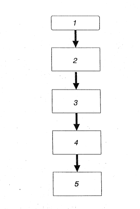
- figure 1 is a flowchart of the steps to be taken in the method -~-
in accordance with the invention,
- figure 2 is a block diagram of a device that performs the method
of the invention, and
- figure 3 shows a block diagram of a possible implementation of
the clock generator of block 11, in accordance with the invention.
DESCRIPTION OF THE INVENTION
The method of the invention is characterized in that the
20 succession of steps shown in the flowchart of figure 1 in which, on ~ - -
block 1, which represents the preamble of the received burst, a ~ -
sampling process 2 is carried out with n samples per bit, by means of n
bit clocks with different Phases. in order to proceed with a ~ -
correlation 3 of this sampled burst preamble 1, with a set of digitized
representations in order to obtain, in this way, the same number of
correlation results as there are representations and then proceed to
the decision 4 for the optimum phase clock, among the n available
:: , ~ :
clocks, and of the first received data bit, based on which is the
result with greatest correlation.
Finally, regeneration 5 takes place of the received data sampled
at the optimum moment, in accordance with the decision 4 taken in the
previous stage.
Next, a device is described that implements the method described -
above, based on the block diagram in figure 2.
In the diagram mentioned, the incoming data 22, that include a
~ 2 1 ~ ~ 7 ~
.: ~ ..
- 4 -
1 preamble with a defined sequence of m bitsl are applied to a first
digitizer 12 to which are also applied the n bit clocks 21 for
digitizing of this preamble. There is also a timing generator 15 that
receives a burst start indication signal 27 and part of the n clocks
36, and that generates, in turn, a first control signal 28 to enable
the first digitizer 12 during a time window in which the defined -
sequence of the burst preamble is expected. -~
When this happens, the digitized preamble 23 appears at the output
of the first digitizer 12 for correlation in a multiple correlator 13
with a certain number of representations of the known sequence of the
burst preamble, also sampled n times per bit and in which each
representation is delayed one sample with respect to the preceding one.
In this way as many correlation results 24 are obtained as there are
representations of the preamble, being analyzed in a selector 14 that
decides, based on which of these is the largest, the optimum phase
clock 25 for the subsequent regeneration of the received data. ~ -
The selector 14 also generates an advance 34 or retard 35 signal
of the burst preamble with respect to the central representation used
in the multiple correlator 13 and a first data bit indication signal
20 33. These burst preamble advance 34 or retard 35 signals are activated,
respectively, when the representatiol that produces the greatest
correlation has been shifted a certain number of samples to the right
or to the left because of a delay that is greater or lesser than that
expected in the reception of the corresponding burst.
This device also incorporates a second digitizer 16 that is
enabled by a second control signal 29, generated by the timing
generator 15, for digitizing the incoming data 22 with the n bit clocks
21, once the preamble has been excluded.
The digitized data 26 coming from the second digitizer 16 are
30 applied over an n-line parallel bus to an output control circuit 17 -~
that also receives the indication of optimum phase clock 25 and the -
indication of the first data bit 33 coming from the selector 14, `
together with a third control signal 30 from the timing generator 15; ~ ~-all the foregoing being used to present at its output the recovered
35 data clock 31 and those data sampled at the optimum instant 32. -
2 1 ~ 8 ~ 9 ~
- 5 -
l In addition, figure 3 shows the composition of the generator 11 oE
the n clocks 21 with different phases, which is done by cascading n-1
delay stages 18, each one producing a delay equal to the bit clock
period divided by n. The n clocks 21 are therefore th~ ou~tputs of
these n-l delay stages 18 plus the input signal to the first stage 37
that comes from a bit master clock. s ~
~ . '"-
'"' :~"'.