Note: Descriptions are shown in the official language in which they were submitted.
141
~~~3k..%ii~c'J
DF-2755
METHOD OF MAKING SYNTHETIC. DIAMOND FILM
FIELD OF THE INVENTION
This invention relates to synthetic diamond and, more
particularly, to a method of making synthetic diamond film.
BACKGROUND OF THE INVENTION
Diamond has a number of properties which make it attractive
for use in various applications. Among these properties are
extreme hardness and excellent transmissivity of certain
radiation. Diamond is also an extraordinary heat conductor,
thermally stable, and an electrical insulator. However, natural
diamond is prohibitively expensive for applications which require
any substantial size ,end is difficult to form into certain
shapes.
In recent years, a number of techniques have been developed
for synthesizing diamond and for depositing synthetic diamond on
surfaces of various shapes to obtain a diamond film or coating.
2d These techniques include so-called high-pressure high-temperature
("HPHT") methods and chemical vapor deposition ("CVD") methods.
The CVD methods include plasma deposition techniques wherein, for
1
2108845
example plasmas of a hydrocarbon and hydrogen are obtained
using electric~~l arcing. The resultant plasma can be focused
and accelerated toward a substrate using focusing and
accelerating magnets.
Synthetic diamond film can be deposited as a permanent
coating on a substrate, such as on the wear surface of a tool
or as an environmentally protective coating. Such films are
generally considered to be relatively thin films.
Alternatively, a synthetic diamond film that is generally
considered a thick film, can be deposited on a substrate and
then removed, preferably intact as a single "free standing"
piece, for usE: in applications such as heat sinks, optical
windows, and in tools. However, the obtainment of such thick
films, especi,~lly of relatively large area, has proven
troublesome. In addition to the difficulty of depositing
quality synthetic diamond of substantial thickness, there is
the problem of removing the diamond intact from the substrate.
The substrate material will generally have a different
coefficient oj= expansion than the diamond, as well as a
different mole~~ular and chemical structure. The adherence and
growth of the diamond film, as well as its release, will
depend, inter alia, on the materials used, surface
2
210885
preparation, and deposition parameters.
Titanium nitride and other materials have been used as a
coating for a substrate, such as molybdenum, upon which synthetic
diamond is to be deposited. Titanium nitride adheres reasonably
well to molybdenum. :Diamond can be deposited over a thin layer
of the titanium nitride and then, ideally, released from the
substrate after the desired thickness of synthetic diamond film
has been deposited, such as by chemical vapor deposition. The
diamond is deposited .at a relatively high temperature and, as the
diamond (as well as t:he titanium nitride interlayer and substrate
below) cools after completion of the diamond deposition, the
diamond should be released from the substrate, preferably in one
piece. However, problems have been found to occur in the
procedure. One of these problems is premature flaking off of the
diamond and/or its underlayer during deposition or premature
release of the diamond before deposition is complete. A further
problem is cracking of the diamond upon its release from the
substrate.
It is among the objects of the present invention to provide
solution to the indicated problems, and to generally improve the
fabrication of free-standing synthetic diamond by chemical vapor
deposition process.
3
2108845
SUMMARY OF THE INVENTION
Applicant has discovered that for obtainment of relatively
thick free standing diamond films having a thickness in the range
200 to 1000 um, the roughness of the substrate surface, beneath
the thin interlayer upon which the diamond is to be deposited by
CVD, should be closely controlled in order to maximize the
efficacy of the diamond deposition and release process. In
particular, the substrate surface roughness must not only be
smooth enough to permit release of the diamond after deposition
of a desired diamond thickness is complete, but also rough enough
to prevent premature lift-off of the diamond or flaking-off of
diamond during the deposition process.
In accordance with an embodiment of the invention, there is
set forth a method for making a free-standing synthetic diamond
film of desired thickness, comprising the following steps:
providing a substrate; selecting a target thickness of diamond to
be produced, said target thickness being in the range 200 microns
to 1000 microns; finishing a surface of the substrate to a
roughness, RA, that ~:s a function bf the target thickness, said
roughness being determined from
0.38t/600 ~Cm 5 RA <- 0.50 ~.m 200 ~,m < t <_ 600 ~,m
0.38 ~.m 5 RA <_ 0.50 ~m 600 ~m < t < 1000 ~m
where t is the target thickness; depositing an interlayer on the
substrate, the interlayer having a thickness in the range 1 to 20
4
B
2108845
microns; depositing synthetic diamond on said interlayer, by
chemical vapor deposition, to about the target thickness; and
cooling the synthetic diamond to effect the release thereof.
In a disclosed embodiment hereof, the step of providing a
substrate comprises providing a molybdenum substrate, and said
step of depositing an interlayer comprises depositing a layer of
titanium nitride. In this embodiment, step of depositing an
interlayer also preferably comprises depositing an interlayer
having a thickness in the range 3 to 5 microns.
As seen from the above indicated relationship between target
diamond thickness and surface roughness, for target thicknesses
between 200 and 600 ~.m the minimum acceptable surface roughness
increases with increasing target diamond thickness. This results
in reducing instances of the types of failure that were first
described above.
Further features and advantages of the invention will become
more readily apparent from the following detailed description
when taken in conjunction with the accompanying drawings.
5
~d .1.. c~' l: ~
BRIEF~DESCRIPTION OF THE DRAWINGS
Fig. 1 is an operational flow diagram of the steps of an
embodiment of the method of the invention.
Fig. 2 is a schematic diagram of a plasma jet deposition
system which can be utilized for CVD deposition of synthetic
diamond for use in an embodiment of the invention.
6
2108845
DETAILED DESCRIPTION
Referring to Fig. 1, there is shown an operational flow
diagram of the steps of a procedure for obtaining free-standing
synthetic diamond film of a desired thickness in accordance with
an embodiment of the invention. The block 110 represents
selection of the target thickness of diamond to be obtained, the
invention being directed to a target diamond thickness in the
range 200 to 1000 microns. The surface of the substrate to be
used for diamond deposition is then finished to a prescribed
roughness, (block 120). The substrate should have a coefficient
of thermal expansion relatively close (preferably within 105/°K)
to that of diamond, and should be a reasonably good thermal
conductor. The preferred substrates hereof are molybdenum,
tungsten, and graphite. Molybdenum (including its alloys such as
TZM, which contains relatively small percentages of titanium and
zirconium) is presently considered particularly preferred. The
surface of the substrate is finished to a roughness, RA [RA being
the universally recognized international parameter of roughness,
which is the arithmetic mean of the departure of the surface
profile from the mean line], as a function of the target diamond
thickness, the roughness being determined from
0.38t/600 ~,m <_ RA <- 0.50 ~,m 200 ~cm < t <_ 600 ~m
0 . 3 8 ~Cm _< RA 5 0 . 5 0 fpm 6 0 0 N.m < t < I 0 0 0 fpm
where t is the target thickness.
7
us i i ~ b t.
'~ ' ~ In
6~.i ~'.. x,! L,' L i :9
A relatively th~:n interlayer, preferably in the range 1 to
20 microns, is then deposited on the finished substrate surface
(block 130),-such as by physical vapor deposition ("PVD"). The
interlayer, which mar if desired comprise several sublayers,
should not bond strongly to diamond. A strong chemical bond will
promote adhesion and ultimately prevent removal of the diamond
from the substrate in one piece. The layer should be thick
enough to prevent chemical bonding of the diamond to the
underlying substrate, and thin enough to maintain the necessary
degree of roughness c>f the coated substrate surface to permit a
degree of mechanical bonding that deters premature release. For
titanium nitride, a preferred interlayer hereof, the layer will
have a thickness in t:he range about 3 to 5 microns. Examples of
other interlayer materials that can be utilized herein are
titanium carbide, hafnium nitride, zirconium nitride, aluminum
nitride, and aluminum oxide. Mixtures and compounds of these
materials can also be utilized.
Synthetic diamond is then deposited, by chemical vapor
deposition, to about the target thickness, as represented by the
block 140. As used herein, deposition to about the target
thickness means deposition to within plus or minus ten percent of
the target thickness. The description below, in conjunction with
Fig. 2, illustrates a technique of CVD plasma jet deposition, but
other techniques of CVD synthetic diamond deposition can be
employed. It can be noted that the invention is particularly
8
i ~~ c-~ ~~ ~ .,
applicable to technic;ues of CVD.synthetic diamond deposition,
such as plasma jet deposition, wherein the diamond is deposited
at a relatively high temperature and subject to substantial
stresses during the deposition and removal processes. After the
target thickness is reached, the synthetic diamond layer can be
released from the sut>strate by cooling, as represented by the
block 150. Release i.s largely due to mechanical stresses upon
cooling, and occurs between about 800 and 400 degrees C. A jet
of nitrogen gas can be directed at the edge of the diamond to
assist the release. In general, when the diamond is released
most of the interlaye~r will remain with the substrate, and any of
the interlayer that is on the diamond can be removed chemically,
such as by selective etching. If the remaining substrate and
interlayer are in sufficiently good condition, they can be used
again a number of times for diamond deposition. When necessary,
the substrate surface can be refinished and recoated with an
interlayer as previously described.
It will be understood that, if desired, the steps of
finishing the surface of the substrate (block 120) and/or of
depositing the interlayer (block 130) can be performed
beforehand, to obtain a supply of substrates and/or coated
substrates from which to choose after the target thickness is
selected. This sequence of steps is equivalent to performing the
finishing and coating of the surface after the target thickness
is selected.
9
4° & C~ r.~? ~ i'
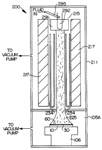
Referring to Fig. 2, there is shown a diagram of a plasma
jet deposition system 200 of a type which can be utilized in
practicing an embodiment of the invention. The system 200 is
contained within a vacuum housing 211 and includes an arc-forming
section 215 which comprises a cylindrical anode 291, a rod-like
cathode 292, and an injector 295 mounted adjacent the cathode so
as to permit injecte~~ fluid to pass over the cathode 292. In the
illustrated system t:he input fluid may be a mixture of hydrogen
and methane. The an~~de 291 and cathode 292 are energized by a
source of electric p~~tential (not shown), for example a DC
potential. Cylindrical magnets, designated by reference numeral
217, are utilized to control the plasma generated at the arc
forming section. Th~~ magnets maintain the plasma within a narrow
column until the plaama reaches the deposition region 60.
Cooling coils 234, in which liquid nitrogen can be circulated,
are located within tlZe magnets and surround the focused plasma.
In operation, a mixture of hydrogen and methane is fed to
the injector 295, and a plasma is obtained in front of the arc
forming section and accelerated and focused toward the deposition
region. The temperal~ure and pressure at the plasma formation
region are typically in the approximate ranges l500-l5,000
degrees C and 100-70() torr, respectively, and in the deposition
region are in the approximate ranges 800-1100 degrees C and
0.1-200 torr, respeci~ively. As is known in the art, synthetic
polycrystalline diamond can be formed from the described plasma,
c v ~? z~,
as the carbon in the methane is.selectively deposited as diamond,
and the graphite which forms is dissipated by combination with
the hydrogen facilitating gas.
The bottom portion 105A of the chamber has abase 106 on
which can be mounted the substrate IO with the titanium nitride
layer 30 on which the synthetic diamond is to be deposited. The
base can include a temperature controller.
rvrarnr nc
A number of samples (about forty) of synthetic diamond film,
with thicknesses in the approximate range 200 to 1000 microns,
were deposited using CVD plasma jet deposition equipment of the
type described in conjunction with Fig. 2. The substrates used
were molybdenum discs of about 6 inch diameter. Some of the
samples were prepared on 3 inch diameter round mesas on the 6
inch discs. The substrate surfaces were lapped with a slurry of
diamond or boron carbide grit to a roughness, RA, ranging from
about 0.33 microns to about 0.51 microns. After coating by PVD
with a titanium nitride interlayer of thickness in the range 3 to
5 microns, equipment of the general type shown in Fig. 2 was used
to deposit synthetic diamond in diameters of about 3 to 4 inches,
and at thicknesses in the approximate range 200 to 1000 microns.
The temperatures at which the diamond released (if no premature
lift-off) were in the range about 800 to 40Q degrees C. Samples
having intended thicknesses of above about 600 um, where the RA
11
21088 4 5
roughness was less th~3n 0.38, had a higher incidence of premature
lift-off, and samples where the RA roughness was greater than
0.50 had a higher incidence of cracking upon release. For
thicknesses less than about 600 ~.m, the minimum roughness needed
to prevent premature release was observed to vary approximately
linearly with thickness as 0.38t/600 ~.m. Further samples were
made in the same mannE~r, but with the substrate first polished to
RA < 0.1 ~Cm. Deposited diamond spalled off before its thickness
reached 75 ~cm .
12