Note: Descriptions are shown in the official language in which they were submitted.
2 1 08868
A PRINTED CIRCUIT BOARD WITH
ELECTRIC ELEMENTS MOUNTED THEREON
This invention relates to a printed circuit board with electric
elements mounted thereon, more particularly to a printed circuit board with
electric elements mounted thereon by the use of at least two different mounting
methods and surface treating methods.
A conventional printed circuit board (PCB) has lands for surface-
mounted devices (SMDs), wherein the lands each comprises a predetermined
pattern of copper foils, and non-electrolysis Ni-Au plates covering the copper
foils.
In mounting SMDs, such as resistance and capacitor chips, small
outline packages (SOPs), connectors, quad flat packages (QFPs), etc. on the
PCB, cream solder is supplied to the lands on the PCB for a re-flow process
carried out by heating the PCB; the SMDs are mounted on the PWD in
accordance with the bonding to the patterned SMD lands. The PCB thus
mounted with the SMDs is connected to an external circuit by using a flexible
printed circuit (FPC) connector.
However, the conventional PCB has the disadvantages that only
packaged devices can be mounted thereon due to the application of heat for the
re-flow process, desired high-density mounting of the SMDs cannot be realized
due to the usage of the FPC connector, and overall thickness, volume and
weight are greater than specified values.
In consideration of the disadvantages described above, an outer-
lead-bonding (OLB) method using tape carrier packages, and a chip-on-board
(COB) method using bonding wires have been adopted in place of the re-flow
method using cream solder, and the FPC connector has been replaced by a
thermal-pressing method providing heat-seal.
In this situation, surface-treatments for PCBs adapted to the above
described methods will be explained below.
~;
21 08868
(1) Non-electrolysis Ni-Au plate
All conventional SMDs can be mounted on a PCB by using
SMD lands covered with the non-electrolysis Ni-Au plates. In this type of PCBs,
although no problem occurs in the thermal-pressing method providing heat-seal,
some problems occur in the OLB method using tape carrier packages and the
COB method using bonding wires. In the OLB method using the tape carrier
packages, one of the problems is the occurrence of bridges among fine- and
narrowly-spaced outer leads, caused by local re-flow of cream solder supplied
on the non-electrolysis Ni-Au plates covering patterned copper foils. In a case
where no cream solder is used, electrodes of tape-automated-bonding (TAB)
devices are required to be plated by non-electrolysis Ni-Au layers, so that the
TAB devices are directly bonded to the PCB. However, this increases the cost
of fabricating device-mounted PCBs due to the adoption of the non-electrolysis
Ni-Au plates on the TAB electrodes. In the COB method using bonding wires,
Au bonding wires are bonded to the non-electrolysis Ni-Au plates of the SMD
lands on the PCB mainly by the bonding between Ni and Au, because the Au
thickness of the non-electrolysis Ni-Au plates is very thin. As a result, the
mechanical strength of the Ni-Au bonding portions is very low, resulting in low
reliability.
(2) Electrolysis solder plate
The electrolysis solder plate has a uniform surface with no
roughness thereon, so that the aforementioned bridges can be avoided, even
if cream solder is supplied on mounting lands to carry out the re-flow process;
but it is difficult to suppress the surplus amount of solder on the PCB. The
electrolysis solder plate can be used in the OLB method using tape carrier
packages without any problem. In other words, although it can be used for the
SMDs and the TABs, it has a problem when used for the COB method with
bonding wires, since the surface uniformity required for the bonding process is
not obtained. Further, the bonding strength among terminals is weak and
unstable due to the usage of solder, thereby resulting in a deterioration in
quality. As a matter of course, electrodes for applying a voltage across plating
-
2 1 08~6~
portions must be provided. As a result of the electrodes, the density of circuitpatterns is lowered.
(3) Soft Au plate
The soft Au plate is basically provided by a chemical
reaction. Therefore, electrodes are needed for the same reason as described
in surface treatment (2). Further, Au plate treatment is required even on the
TAB side in the OLB method using tape carrier packages. As a result, an
increase in cost is inevitable.
As discussed in surface treatments (1) to (3), devices or parts
mountable on a PCB are limited in kind, depending on the type of plating layer
that is used on the PCB. Consequently, it is difficult to fabricate a PCB havingmounted electric elements and that has a high density, a thin and compact
configuration, and high quality.
Accordingly, it is an object of the invention to provide a PCB with
electric elements mounted thereon in which an element-mounting density is
high, and in which a thin and compact-size configuration is realized.
It is a further object of the invention to provide a PCB with electric
elements mounted thereon and improved reliability.
In one form, the invention is a printed circuit board that comprises
electric elements mounted thereon by using at least two methods selected from
a re-flow method using supplied cream solder, a chip-on board method using
bonding wires, an outer lead bonding method for mounting a tape carrier
package, and a thermal pressing method providing heat-seal. The electric
elements are mounted on the printed circuit board by using lands provided
thereon. The lands comprise a land having a non-electrolysis Ni-Au plate
surface-layer which is used for the re-flow and thermal pressing methods, a landhaving a soft Au plate surface-layer which is used for said chip-on board
method, and a land having an electrolysis solder plate surface-layer which is
used for the outer lead bonding method.
In another form, the invention is a printed circuit board that
comprises lands for mounting electric elements thereon. The lands have a
2 1 0~868
structure dependent upon which of a plurality of methods is used to mount
electric elements on the printed circuit board. The lands have a structure that
comprises a predetermined pattern of a copper foil covered by a non-electrolysisNi-Au plate when a re-flow method using cream solder is used, or a thermal
5 pressing method is used. The lands have a structure that comprises the
predetermined pattern of a copper foil covered by the non-electrolysis Ni-Au
plate, which in turn is covered by an electrolysis solder plate when an outer lead
bonding method is used to mount a tape carrier package. The lands have a
structure that comprises the predetermined pattern of a copper foil covered by
10 the non-electrolysis Ni-Au plate, which in turn is covered by a soft Au platewhen a chip onboard method is used to mount the electric elements on the
printed circuit board. The electric elements may comprise at least two electric
elements selected from a resistance chip, a capacitor chip, a semiconductor
device package, and a connector.
In a still further form, the invention is printed circuit elements
formed with a predetermined pattern on the printed circuit board, and lands
provided on the printed circuit board. The lands are connected to the printed
electric circuits. A land has a non-electrolysis Ni-Au plate surface layer to beused for a re-flow and thermal pressing methods to mount electric elements on
20 the printed circuit board. A land has a soft Au plate surface layer to be used for
a chip onboard method to mount electric circuit elements on the printed board.
A land has an electrolysis solder plate surface layer to be used for an outer lead
bonding method to mount electric elements on the printed circuit board.
In yet a further form, the invention is a method of fabricating a
25 printed circuit board comprising lands for mounting a plurality of electric
elements on the printed circuit board. The lands comprise a predetermined
pattern of a copper foil covered by a non-electrolysis Ni-Au plate. The method
comprises the first step of covering the non-electrolysis Ni-Au plate of some ofthe lands with an electrolysis solder plate surface layer to allow a tape carrier
30 package to be mounted by a local re-flow method on the lands covered by the
electrolysis solder plate. A second step is to cover the non-electrolysis Ni-Au
.~
,,, ~
21 0~8~
plate of some of the lands with a soft Au plate surface layer to allow the electric
elements to be mounted by a chip onboard method on the soft Au plate surface
layer covered lands using bonding wires. A third step involves mounting some
of the plurality of electric elements on some of the lands covered by the non-
electrolysis Ni-Au plate surface layer by a local re-flow method using cream
solder. A final step involves mounting some of the plurality of electric elements
on some of the lands covered by the non-electrolysis Ni-Au plate surface layer
by a thermal pressing method providing heat-seal.
The invention will next be explained in greater detail in conjunction
with the appended drawings, wherein:
Figures 1A to 1 C show a conventional PCB with electric elements
mounted thereon, wherein Figure 1A is a top surface perspective view, Figure
1B is a bottom surface perspective view, and Figure 1C is a cross-sectional
view;
Figures 2A to 2C, and Figures 3A to 3C show PCBs with electric
elements mounted thereon in first and second preferred embodiments according
to the invention, respectively, wherein Figures 2A and 3A are top surface
perspective views, Figures 2B and 3B are bottom surface perspective views,
and Figures 2C and 3C are cross-sectional views; and,
Figures 4A and 4B, Figures 5A and 5B, Figures 6A and 6B,
Figures 7A and 7B, Figures 8A and 8B, Figures 9A and 9B, Figures 10A and
10B, Figures 11A and 11B, Figures 12A and 12B show PCBs mounted with
electric elements thereon in third to eleventh preferred embodiments according
to the invention, respectively, wherein Figures 4A to 12A are top surface-
perspective views, and Figures 4B to 12B are bottom surface-perspective views.
Before a first preferred embodiment of a PCB with electric
elements mounted thereon is explained, the aforementioned conventional PCB
with electric elements mounted thereon will be explained.
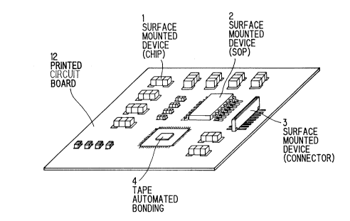
Figure 1A shows the conventional PCB 12, on the top surface of
which are various SMDs, including chips 1 such as resistors and capacitors
molded of ceramic, plastic, etc., a SOP 2 which is packaged by plastic, etc., a
2 1 0886~
connector 3 for connecting internal circuits on the PCB to external circuits, and
a QFP 12.
Figures 1 B and 1C show the PCB having a through-hole (only in
Figure 1C) and SMD lands 5, wherein each of the SMD lands 5 comprises a
5 predetermined pattern of a copper foil 51 and a non-electrolysis Ni-Au plate 52
functioning as a surface-treating layer; Figure 1 C does not correspond to Figure
1B precisely.
In fabrication, cream solder is supplied on the SMD lands 5 on the
PCB 12, and the SMDs 1, 2, 3 and 9 are positioned thereon. Then, thermal
10 treatment is carried out by heating the PCB 12 at a predetermined temperature.
Thus, a re-flow process takes place to fabricate the PCB 12 with electric
elements mounted thereon.
Figure 2A shows a first preferred embodiment of a PCB with
electric elements mounted thereon, wherein like parts to those used in Figure
15 1A are indicated by like reference numerals.
In the first preferred embodiment, a TAB for mounting a tape
carrier package 4, which is a semiconductor device other than an IC and LSI,
is provided on the PCB 12 in addition to the aforementioned SMDs 1, 2 and 3.
Figures 2B and 2C show the PCB 12 (with a through-hole being
20 only shown in Figure 2C), SMD lands 5 and a TAB land 6, wherein the TAB
land 6 comprises a predetermined pattern of a copper foil 61, a non-electrolysisNi-Au plate 62, and an electrolysis solder plate 63.
In fabrication, the TAB package 4 is mounted on the TAB land 6
by the OLB method, so that the tape carrier package is mounted on the PCB 12
25 in accordance with a local re-flow process of the electrolysis solder plate 63,
using no cream solder. On the other hand, the SMDs 1, 2 and 3 are mounted
in the same manner as in Figures 1A, 1B and 1C.
Figure 3A shows a second preferred embodiment of a PCB 12 with
electric elements mounted thereon, wherein like parts to those used in Figures
30 1A and 2A are indicated by like reference numerals.
~.'
21 û88~
In the second preferred embodiment, a COB device 7 (a pair of
ICs) is on the PCB 12 in addition to the SMDs 1, 2 and 3.
Figures 3B and 3C show the PCB 12 (with a through-hole being
only shown in 3C), SAD lands 5 and a COB land 8, wherein the COB land 8
comprises a predetermined pattern of a copper foil 81, a non-electrolysis Ni-Au
plate 82, and a soft Au plate 83.
In fabrication, the pair of ICs are mounted on the PCB 12 by using
Au bonding wires (not shown) for bonding to the soft Au solder 83 of the COB
land 8. On the other hand, the SMDs 1, 2 and 3 are mounted on the PCB 12
in the same manner as in Figures 1A, 1B and 1C.
Figure 4A shows a third preferred embodiment of a PCB 12 with
electric elements mounted thereon, wherein like parts to those used in Figures
1A, 2A and 3A are indicated by like reference numerals.
In the third preferred embodiment, a heat-sealed connector 10 is
provided on the PCB 12 for connecting internal circuits on the PCB 12 to
external circuits.
Figure 4B shows the PCB 12, having SMD lands 5 and a heat-seal
land 11, wherein the heat seal connection is realized in accordance with local
re-flow of a non-electrolysis Ni-Au plate, as shown in Figure 1C, functioning asa surface-treating layer by means of a thermal-pressing method using thermal-
setting adhesive.
Figure 5A shows a fourth preferred embodiment of a PCB 12 with
electric elements mounted thereon, wherein like parts to those used in Figures
1A to 4A are indicted by like reference numerals.
Figure 5B shows the PCB 12 having a TAB land 6 and a COB land
8 as previously explained.
Figure 6A shows a fifth preferred embodiment of a PCB 12 with
electric elements mounted thereon, wherein like parts to those used in Figures
1A to 5A are indicated by like reference numerals.
Figure 6B shows the PCB 12 having a TAB land 6 and a heat-seal
land 11 as previously explained.
~A
21 0~6~
Figure 7A shows a sixth preferred embodiment of a PCB 12 with
electric elements mounted thereon, wherein like parts to those used in Figures
1A to 6A are indicated by like reference numerals.
Figure 7B shows the PCB 12 having a COB land 8 and a heat-seal
land 11 as previously explained.
Figures 8A and 8B show a seventh preferred embodiment of a
PCB 12, wherein a TAB package 4, a COB-IC 7, and a heat-sealed connector
10 are mounted on the PCB 12 by the OLB method using a tape carrier
package; the COB method uses Au bonding wires, and the thermal pressing
method provides a heat-seal, as described before. The TAB land 6 has an
electrolysis solder plate, the COB land 8 has a soft Ni-Au plate, and the heat-
seal land 11 has a non-electrolysis Ni-Au plate, respectively, as surface-treating
layers.
Figures 9A and 9B show an eighth preferred embodiment of a PCB
mounted with ICs, wherein resistor and capacitor chips 1 and a connector 3, a
TAB package 4, and a COB-IC 7 are mounted on the PCB 12 by the re-flow
method using cream solder, the OLB method for mounting a tape carrier
package, and the thermal-pressing method providing heat-seal, respectively.
The SMD lands 5 have a non-electrolysis Ni-Au plate, the TAB land 6 has an
electrolysis solder plate, and the COB land 8 has a soft Au plate, respectively,as surface-treating layers.
Figures 10A and 10B show a PCB with electric elements mounted
thereon in the ninth preferred embodiment. Resistor and capacitor chips 1 and
a SOP 2, a TAB package 4 and a heat-sealed connector 10 are mounted on the
PCB 12 by the re-flow method using cream solder, the OLB method for
mounting a tap carrier package, and the thermal pressing method providing
heat-seal, respectively. The SMD lands 5 and the heat-seal land 11 have non-
electrolysis Ni-Au plates and the TAB land 6 has an electrolysis solder plate,
respectively, as surface-treating layers.
Figures 11A and 11 B show a PCB with electric elements mounted
thereon in the tenth preferred embodiment. Resistor and capacitor chips 11, a
,~ ~
2 1 08868
SOP 2, a COB-IC 7, and a heat-sealed connector 10 are mounted on the PCB
12 by the re-flow method using cream solder, the COB method using Au
bonding wires, and the thermal-pressing method providing heat-seal,
respectively. The SMD lands 5, and the heat-seal land 11 have non-electrolysis
5 Ni-Au plates, and the COB land 8 has a soft Au plate, respectively, as surface-
treating layers.
Figures 12A and 12B show a PCB with electric elements mounted
thereon in the eleventh preferred embodiment. Resistor and capacitor chips 1,
a TAB package 4, a COB-IC 7, and a heat-sealed connector 10 are mounted
10 on the PCB 12 by the re-flow method using cream solder, the OLB method for
mounting a tape carrier package, the COB method using Au bonding wires, and
the thermal-pressing method providing heat-seal, respectively. The SMD lands
5 and the heat-seal land 11 have non-electrolysis Ni-Au plates, the TAB land 6
has an electrolysis solder plate, and the COB land 8 has a soft Au plate,
15 respectively, as surface-treating layers.
Although the invention has been described with respect to specific
embodiments for complete and clear disclosure, the appended claims are not
to be thus limited, but should be construed as embodying all modifications and
alternative constructions that may occur to one skilled in the art which fairly fall
20 within the basic teaching herein set forth.