Note: Descriptions are shown in the official language in which they were submitted.
WO 93/18581 ~ Q (~ ~ s pCT/EP93/00430
This invention relates to a radio frequency power
amplifier employing a linearization technique.
Future mobile radio systems will be required to improve
their spectral efficiency beyond that which currently exists
today. This will mean that modulation schemes in which the
information is carried in both the transmitted signal
amplitude and phase will increasingly become required. In
order to canserve spectrum and to coexist with current radio
systems the transmitters using these complex modulations will
have to be linear. For example adjacent channel interference
levels of > -60dBc in a 25kHz channelisation may be required.
nmmary of the Prior Art
One technique to achieve such power amplifier linearity
performance is Cartesian feedback. This technique has become
popular as it lends itself to integration on IC's.
The requirement for linearity (determined by adjacent
channel interference limits) and maximum power efficiency,
means that the power amplifier will have to operate as close
to the gain compression (clip) point as possible, but still
retain required level of linearity.
A known technique to measure and adjust for maximum
phase margin of the closed loop system and to identify the
clip point of the amplifier uses an appropriate training
sequence. Gain compression is detected by an increase in the
magnitude of the Cartesian loop error signal above a given
threshold. At this point the drive level control circuits
are set appropriately and linear operation is assured - i.e.
input signal is backed of.f.
The above technique is only suitable in future radio
products where time is available for training prior to each
WO 93/18581 ~ ~ ~ ~ d ~ ~ '. PL'f/EP93/00430
transmission. Time delays generally required to implement
training are in the order of milliseconds. To allow this
linearization technique to be implemented in systems where no
training time is allocated,, ow alternative approach is ,
required.
In addition to achieving linearity through training, .
there is a need for improved methods of maintaining
linearity.
Summary of the Invention
According to the invention, there is provided a radio
transmitter comprising: a power amplifier; linearizing means
for compensating for non-linearity in the power amplifier;
and feedback means for feeding a signal from an output of the
power amplifier to the linearizing means for maintaining
linearity, said amplifier, linearizing means and feedback
means forming a loop having adjustable loop linearization
parameters; a look-up table for storing predetermined loop
linearization parameters; and control means having an
operating condition input, said control means being coupled
to the look-up table and the loop for selecting a loop
linearization parameter in response to a transmit control
signal according to an operating condition input to the
central means at the time of receipt of the transmit control
signal.
The loop linearization parameters may be phase and/or
gain parameters.
The operating condition input may be channel frequency,
battery level, temperature or other information. A separate
table may be stored for different values for each of these
parameters. Thus, when operating at half the battery level,
a table may be selected relating to that battery level.
There is preferably a temperature input receiving a
signal from a temperature sensor. .
The tables preferably have settings for both phase and
gain parameters.
In a particularly preferred feature of the invention,
the look-up table is updated by measuring the actual loop
V6~0 93/18581 ~ ~ ~ ~ ~ ~ ~ PCT/EP93/00430
3
linearization parameter, selecting an improved linearization
parameter and writing the improved parameter into the look-up
table. In this manner, the accuracy of the look-up tables
can be maintained with time. Moreover, by continuously
updating the look-up tables, it is not necessary to stare as
extensive a range of linearization parameters for different
operating conditions.
A phase setting is particularly sensitive to changes in
operating conditions and the look-up tables may contain more
phase parameter information than gain parameter information.
In particular, if the phase margin can always be maintained
at a maximum level, reduced adjacent channel splatter is
observed.
For continuously measuring the phase and/or gain or
other parameter of the loop, it is particularly preferred
that receiver means are provided tuned to an adjacent
transmitter channel for measuring modulation on the adjacent
channel.
The adjacent channel receiver means may take the form of
an adjacent channel receiver coupled to the output of the
power amplifier and dedicated to the purpose of measuring the
transmitter adjacent channel power. Alternatively, the
adjacent channel receiver means may take the form of a
receiver switchable between a first receive frequency which
is separated from the frequency of the signal from the power
amplifier by a duplex separation frequency and a second
frequency which represents the frequency of a channel
adjacent to that of the signal from the power amplifier.
In the latter of the above embodiments of adjacent
channel receiver means, it is preferred that control means
are provided for switching the receiver between a receive
frequency on a receive timeslot and an adjacent channel
frequency on a transmit timeslot and back to the receive
frequency on a subsequent receive tirneslot.
Attenuator means may be provided switchable into a path
between the power amplifier and the adjacent channel~receiver
for attenuating the signal from the power amplifier to the
adjacent channel receiver during transmission and for passing
V1~~ 93/18581 PCT/EP93/00430
y
an unattenuated signal from an antenna during a receive mode
of operation.
~~ef Degcription of the Drawines
,
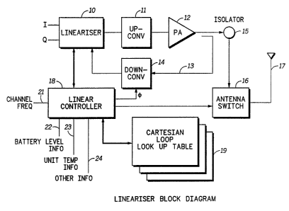
Fig. 1 shows a block diagram of a radio transmitter with
power amplifier and l.inearizer in accordance with a first
embodiment of the invention.
Fig. 2 shows a block diagram of a radio transmitter with
power amplifier and linearizer in accordance with a second
embodiment of the invention.
Fig. 3 shows switched attenuator circuit for switching
into the circuit of Fig. 2 at point (b).
Fig. 9 shows a TnMA tinning format in which the invention
may be employed.
n
Referring to Fig. 1, there is shown a radio transmitter
comprising a linearizer 10, an upconverter 11, a power
amplifier 12, a feedback loop 13, and a downconverter 14.
The output of the power amplifier 12 is connected via an
isolator 15 and an antenna switch 16 to an antenna 17. A
linear controller 18 is provided connected to the linearizer
10, the downconverter I4 and the antenna switch 16.
Connected to the linear controller 18 is a series of look-up
tables in memory 19. The linear controller 18 has a number
of inputs of which a channel/frequency input 21, a battery
level input 22, a unit temperature input 23 and other
information inputs 24 are shown.
On accepting a request for transmission from a push-to-
talk (PTT) switch (not shown) or otherwise, the transmitter
power amplifier 12 is turned on. The various operating
parameter inputs 21, 22 and 23 are measured by the controller
18 and a look-up table 19 is selected for the measured
conditions. Thus, for a particular channel, battery level and
measured temperature (as indicated by a temperature sensor),
predetermined gain and phase settings will be downloaded from
the look-up table 19.
WO 93/18581 ~ ~ fl ~ ~ ~ ~ PGT/EP93/00430
S
The linearizer phase shift and drive level attenuator
settings, which are described in more detail in the paper
"Transmitter Linearization using Cartesian Feedback for
Linear TDMA Modulation" by M Johansson and T Mattsson 1991,
IEEE are set in the downconverter 14 and the linearizer 10
respectively by the linear controller 18 depending on the
values read from the look-up table 19. The antenna switch 16
is at this point operated using an appropriately controlled
ramp signal, having a raised cosine profile, to avoid excess
splatter to adjacent channels. Transmission of the
information (data or voice) defined by I and Q samples input
to the linearizer 10 now takes place in a stable linear
operation.
The values in the look-up table 19 are set in the
factory by extensive testing at different temperatures
battery levels, etc.
In a more preferred embodiment of the invention, the
values in the look-up table are updated as the radio is used.
For a given transmission request, the loop phase and
gain parameters read from the look-up table 19 are those set
in the look-up table from a previous transmission on the
channel in question at the battery level and temperature in
question. When these values have been loaded into the
linearizer 10 and transmission begins, a comparison is made
between the I and Q values input and those received on the
feedback loop 13 from the downconverter 14. Based on a
comparison of these values, a decision is made as to the need
for updating the loop phase and gain parameters. If, for
example, the phase margin has decreased, a new phase setting
is calculated to increase the phase margin for the loop.
This new phase setting is now written into the particular
location in the look-up table 19 for the current channel,
battery level and temperature 'settings and replaces the
previously existing value. The new value will be used next
time a transmission is requested on that channel at that
battery level and at that temperature.
An assumption is made that changes in loop phase and
gain characteristics due to battery voltage and temperature
are independent of one another. This allows separate look-up
. ... ,; .:. . "... . , ~;;, ... ,. . : . ..;.. v; : , :.. w..;:- ...: A~ ,.;
_.. -. ..
.. _,. . .... .. . ;.,,... ,... ..~~.~., .
WO 93/18581 ~ ~ ~ ~ ~ ~ 3 PCT/~P93/00430
tables to be used for different battery voltage settings and
temperature settings. It is found that this is a workable
assumption, however, more extensive look-up tables can be
stored for particular battery level and temperature pairs.
T
The memory 19 can be arranged in other formats.
Interpollation may be carried out between values, e.g. values
for measurements at two temperature when the temperature
sensor senses an intermediate temperature.
To allow for the linearizer adjustment, the ramp signal
to the antenna switch is delayed by an appropriate amount Ot;
this is to compensate for the look-up table access time and
downloaded to the linearizer circuitry. This delay is
assumed to be minimal in comparison with the ramp time of the
antenna switch. Therefore when the antenna is connected to
the power amplifier output, the power amplifier is operating
at the correct level to ensure compliance with required
interference specifications.
As an alternative to sensing of loop gain and phase
settings and refreshing the look-up table entries after each
transmission, a retraining sequence can be input to the
linearizer 10 and transmitted out of the antenna 17, or into
a load as described in co pending UK patent application
............. entitled °'Radio Transmitter with Linearization
Training Sequence" file don the same date as the present
application, or transmitted. into an adjacent channel receiver
as is described~below,
The sensing of loop gain and phase settings and
refreshing of the look-up table entries after each
transmission does not incur a time penalty and allows the
transmitter to be available at all times. The values in the
tables can be refreshed when a measured value deviates from a
stored value by more than the predetermined amount, or they
can be refreshed at regular intervals.
If retraining is used, this can be implemented by
refreshing the look-up table entries on every power-up of the ,
radio, by refreshing the look-up table entries at fixed
intervals of operation in terms of absolute time or
transmission time, or refreshing the look-up table entries at
intervals dictated by radio transmitter conditions.
CA 02109063 2002-02-13
WO 93/18581 PGT/EP93/00430
Loop phase and drive level settings are monitored and
adjusted during transmission to take into account changing
device characteristics and the linearized power amplifier is
optimized for both stability and efficiency. The transmitter
_ efficiency is maximized by operating the power amplifier as
close to its gain compression point as possible, as described
in US Patent No. 5,239,692 issued August 24, 1993, to
Motorola Inc. The transmitter, however, is restricted by the
amount of adjacent channel interference it should be
allowed to generate. For maximum efficiency the transmitter
must operate as close to the adjacent channel interference
limit as possible. It would be desirable to provide an
improved means for performing a "clip detect" operation to
find the optimum setting of loop gain for the feedback
network. .
An arrangement is shown in Fig. 2 which meets the above
need and comprises a number of elements already described
with reference to Fig. 1. In Fig. 2, there is shown a
microprocessor 30 which controls the gain (A) and phase (m)
of the feedback loop. In Fig. 2, a phase adjuster 31 is
shown separate to the linearizer 10, as is a feedback phase
detector 32. It will be appreciated that these elements are
present in the circuit of Fig. 1, but are merely encompassed
within the linearizer block 10 of Fig. 1.
In addition to the above elements, the circuit of Fig. 2
has an adjacent channel receiver 33, or in a further
embodiment, as an alternative to adjacent channel receiver
33, a subscriber receiver 34 is provided, with a control input
from microprocessor 30 for changing the receive frequency of
the subscriber receiver 34 from a receive mode (for receiving
voice/data from the antenna 17~ to wn adjacent channel
receive mode for measuring adjacent channel receive power.
Referring to the first of these alternative embodiments,
the adjacent channel receiver 33 is connected to the output
of the power amplifier 12 and comprises an attenuator, a
downconverter to a suitable IF frequency, a mixer which taps
a signal from a main synthesizer for the radio, an IF filter,
an attenuator, a rectifier and means for measuring voltage
across the rectifier. A ceramic filter is suitable for the
WO 93/18581 ~ ~ ~ C~ ~ ~ ~ ~ PGT/E1'93/00430
a
8
IF filter. This ceramic filter is a 2.5 KHz bandpass filter
tuned to a frequency 2,5KHz affset from the IF signal for the
corresponding transmit channel.
In the second embodiment shown in Fig. 2 in which the
subscriber receiver 34 changes between a receive mode and an
adjacent channel receive mode, operation will be described
with reference to a TDMA system having 60 millisecond frames
divided into 4 timeslots of 15 milliseconds each as shown in
Fig. 9. A transmit frame is always offset from a receive
frame and vice versa. A channel pair may comprise the first
timeslot of the transmit frame and the first timeslot of the
receive frame or the second timeslot of the transmit frame
and the second timeslot of the receive frame etc. There will
always be about 15 milliseconds between the end of a transmit
timeslot and the beginning of a receive timeslot. This
provides ample time for the microprocessor 30 to provide a
control signal to the synthesizer of the subscriber receiver
34 to cause a receive frequency change equal to the duplex
frequency separation between the transmission receive
frequencies less (or in addition to) an amount equal to the
channel spacing. Where the duplex frequency separation is
lOMHz, and the channel separation is 25 KHz, the signal from
the microprocessor causes the receiver 39 to change its
receive frequency through 9.975 MHz or 10.025 MHz. After a
receive frame, the receiver 34 changes its frequency to be
adjacent that of the signal being transmitted from power
amplifier 12 in a transmit frame and, after transmission, it
switches back to its appropriate receive frequency for
receiving the next timeslot from the antenna 17.
While the adjacent channel receiver 33 or the re-tuned
subscriber receiver 34 is tuned to the adjacent channel, it
is able to measure the power on the adjacent channel. If the
level of signal on the adjacent channel exceeds a threshold,
for example a threshold of 60 or 63 dB below the output level
of the power amplifier 12, this is an indication of onset of
clipping in the power amplifier 12 and an indicatiari that it
is necessary to back off the gain,of the power amplifier 12.
Thus, the adjacent channel receiver 33 or the subscriber
receiver 39 provides a signal to the microprocessor 30 from
~~~~~~J
WO 93/18581 PCT/EP93/00430
9
which, if onset of clipping is detected, controls the
linearizer 10 to reduce the gain A.
As a result, with a real-time knowledge of the splatter
to adjacent channel power, backing off made to the drive
level to the power amplifier can be minimised at all times
ensuring true optimum operating efficiency. In addition, the
arrangement ensures a predetermined maximum splatter into the
adjacent channel at all times.
On detecting of clipping and backing off of the power
amplifier, the new value for the loop gain (a) can be loaded
into the look-up tables of Fig. 1.
The adjacent channel receiver of 33 or subscriber
receiver 34 can be used for detecting "clip" during a
training sequence such as that described in US Patent No.
5066923 of Motorola Inc. During the training sequence, the
energy of the power amplifier is diverted into the adjacent
channel receiver 33 or the subscriber receiver 34 by
isolation of the antenna 17 using the antenna switch 16.
This allows the energy to be directed away from the antenna
ensuring "off-air" training and no on-air adjacent channel
splatter. It is proposed that this transmit energy whilst
training is diverted into the appropriate receiver by the
microprocessor 30 controlling the antenna switch 16. This
can be achieved by:
(1) coupling of some-of the feedback signal power into a
separate receiver tuned to the adjacent channel or
(2) short circuiting the antenna switch into the
subscriber unit receiver and switching the down-converter
local oscillator frequency by the duplex separation frequency
plus or minus the channel bandwidth, therefore allowing the
standard receiver to perform a received signal strength
indication on the adjacent transmit channel.
In the case of a short circuited implementation,
suitable attenuation of the transmitter power is required to
avoid over driving the receiver. This is implemented by
appropriate switching of receiver paths 40 and 41 as~shown in
Fig. 3. Receiver path 40 provides a path from the antenna 17
to the receiver 34. Adjacent channel receive path 41
provides a path in the case of routing of the signal from the
WO 93/18581 3 PGT/EP93/00430
,~pgp6
ro
power amplifier 12 to the receiver 34. The circuit comprises
three pin diode switches 16, 93 and 49 under control of the
microprocessor 30. An attenuator 45 is provided in the
adjacent channel recei..ve path 41, having a suitable value to
avoid overdriving the receiver circuitry. The operation is as
follows. Simultaneously with the switching of the antenna
switch 16 by the microprocessor controller 30, the controller
30 causes pin diode switches 93 and 49 to switch from path 40,
to path 41, thus switching attenuator 45 into the path to
protect the receiver. The timing can be arranged such that
attenuator 45 is always switched into the path before antenna
switch 16 switches
The measurement of the adjacent channel power in the
adjacent channel receiver can be accomplished by any.of the
standard methods available. One of which is to use an FFT of
the received signal, and then processing this data to obtain
a measurement of the adjacent channel power. The generation
of the transmit spectrum has the advantage over the
previously described method of using the a separate adjacent
channel receiver for measuring the adjacent channel power as
it is able to monitor both adjacent channels simultaneously.
The invention also allows a method of real-time
monitoring of the phase shift around the feedback loop, thus
allowing the loop phase to be adjusted whenever required,
ensuring stability at all times. This technique can be
utilised to reduce the phase margin normally designed into
such feedback systems, therefore creating an opportunity to
increase the loop gain and consequently improve the
intermodulation performance that is attainable by significant
amount.
It is proposed that some of the feed-back signal is
routed into a phase detector, which then transmits the phase
information of the feed-back signal to the microprocessor.
This phase measurement can then be compared against the phase
of the transmitted signal (which is also measured). Any ,
transmit data is suitable for use with this phase comparison.
It is suggested that for continuous operation mode within
current TDMA frame structures, that measuring the phase shift
of the synchronisation word is a good option.
WO 93/18581 '~ ~ o ~ Q ~ ~ PCT/EP93/00430
t1
Phase shift measurement during the synchronisation word
is carried out at the beginning of a timeslot when the
synchronisation work is transmitted in terms of predetermined
I and Q samples being input to linearizer 10. These
predetermined I and Q samples can be used for comparison with
the corresponding samples measured by downconverter 14.
Thus, the phase shift measurement is carried out during
transmission of the synchronisation word.
The overall arrangement described provides the
advantages of:
(1) providing a method of "clip detection" by measuring
the splattered power transmitted into the adjacent channel as
part of a training process or as a real-time measurement of
the intermodulation performance of the loop:
(2) providing an alternative method of measuring the
phase shift around the feedback laop during continuous
operation and during a training process and
(3) maximising the operating efficiency of the power
amplifier by operating as close as possible to its saturation
level whilst maintaining a satisfactory intermodulation ratio
performance.
Instead of using Cartesian feedback, predistortion
feedback can be used as described in the paper "Linear
Amplification Technique for Digital Mark Communications" by
Yoshinori Nagata 1989 IEEE. In this case parameters other
than gain and phase will be stored in the look-up table.
Instead, I and Q sample predistortion factors or parameters
will be~stored.
,. .,.., ,.. ..".,.... ,., r ...,.t.. .\.:o.S . ... . ... ..."..