Note: Descriptions are shown in the official language in which they were submitted.
wo 93/18583PCr/us93/00225
-1-
2109410
HIGH EFFICIENCY DUAL MODE POWER AMPLIFIER
APPARATUS
Fi~doftbe I~ti~
s
The present invention relstes generally to the field of
~mplifiers and particularly to dual mode power ~mplifi~rs.
Bac4~und of 1be I~_.lion
The rapid e~p~n~ion of the number of cellular radio-
telep~nes coupled with the desire to provide additional ser-
vices has l,~om~l,ed the use of an i~ o~ed tr~ncmi~siQn
te~hnique, time division multiple access (TDMA). TDMA in-
15 creases system capacity over the current ~n~loE systemthrough the use of digital mod~ tio- and s~ee~h coding tech-
niques. A TDMA tr~ncmi~sion is com~,;sed of many time
slots.
A linear mod~ ti~n technique"~J4 differential quadra-
2 0 ture phase shift keying (r~/4 DQPSK), is used to transmit thedigital information over the ~h~nnel The use of linear modu-
lation in the U.S. Digital Cellular system provides spectral ef-
ficiency allowing the use of 48.6 kbps ch~nnel data rates. 7~J4
DQPSK transmits the data inform~tiorl by eIlro~ling cQn~ectl-
2 5 tive pairs of bits, commonly known as symbols, into one of fourphase angles (~/4, ~37c/4) based upon gray enco~ing. These
angles are then differentially enco~letl to produce an 8 point
constellation.
Transmitters ~lçsi~ne~l for use in the U.S. Digital
3 0 Cellular system are required to operate in both the analog and
digital modes. The digital mode uses the 7~J4 shift DQPSK
mod~ tior, and can be implemented using a linear transmit-
ter. The analog mode uses conventional frequency modula-
tion and allows the use of higher efficiency non-linear trans-
3 S mitters.
WO 93/18583 PCI/US93/00225
~109 41~ -2-
Conventional linear ~mplifiers are inherently less effi-
cient than their constant envelope counterparts due to the
types of siPne-ls they must amplify. A constant envelope am-
plifier is required to put out a signal at only one power level
over time. It ~o-n therefore be optimi7e~ for peak efficiency at
that power level. This optimi7o-tiQn çntoilR pl-o-cinE a load
impetl~nce on the device such that, at the ~1esienerl power out,
the AC collector voltage magnitude is close to or even e~cee~
the DC supply voltage. In this condition, the ~mplifier is close
to or actually in saturation and has ol,ti ~ efficiency.
The linear ~omplifier must amplify si~nols at power
levels that vary over time, with whatever amplitude modula-
tion that has been i ~,essed upon the input si~n~l No satu-
ration is allowed in the linear ~mplifiPr~ or there will be se-
1 5 vere distortion of the envelope. This distortion c~lses 1088 of
amplitude information and spre~lin~ of the transmit spec-
trum into adjacent rh~nnPl~. The ~mrlifier circuit must op-
erate such that at peak power out, the ~mrlifier is not in satu-
ration. While it is possihle to optimi7e for good efficiency at
2 0 peak power out, the çffiriPnry falls off rapidly as power out
falls.
This creates a problem for the U.S. Digital Cellular ra-
dio which is int~n~ to operate in both linear and constant
envelope mo-les. When comp~red to current ~n~loE radios
2 5 with constant envelope ~mplifiers~ çfficiency will be much
lower in the digital radio. In the linear mode, efficiency is op-
timi7efl for peak power out, but the signal spends only a short
time there. Average efficiency will be lower than peak power
efficiency because of this. For digital cellular this is not a se-
3 0 vere limitation since a TDMA system is used and the trans-
mitter is only on V3 of the time (only every third time slot is
used by the radio). Even if the average effiriçncy is poor in this
mode, transmit current is not signific~ntly worse (and may be
better) than a conventional analog radio.
3 5 The problem arises when this same radio is used for an
analog call with a constant envelope signal. Now the trans
- ~ 0~4 ~ ~
- 3 -
mitter is on for 100% of the conversation time and, since it operates at
an average power 3.2 dB below the optimum power out, efficiency is
poor. Data on test circuits shows drops in the 12 percentage point
range. This translates into a substantial increase in transmit current.
The increased current requirements will substantially decease the time
that a battery powered radiotelephone will be useful. There is a
resulting need for an amplifier circuit that operates efficiently in both
linear and constant envelope modes.
Summary of the Invention
0 In accordance with the present invention, there is provided a dual
mode power amplifier apparatus comprising at least one amplifier having
a collector supply input, a signal input and an output, and a switching
power supply having a mode select input, a power input and an output.
The amplifier generates a signal at the output that has amplified
characteristics of an input signal coupled to the signal input. The
switching power supply is off in a first mode, thereby allowing a signal
at the power input to pass through to the output, and the switching
power supply is on in a second mode, thereby supplying a
predetermined voltage to the switching power supply output. The first
and second modes are selected in response to a mode select signal
coupled to the mode select input. The switching power supply output
is coupled to the supply input of the amplifier.
Brief Description of the Drawings
FIG. 1 shows the preferred embodiment of the dual mode power
amplifier apparatus of the present invention.
FIG. 2 shows another embodiment of the dual mode power
amplifier apparatus of the present invention.
FIG. 3 shows a flowchart of the method of the present invention.
4 ~ ~
FIG. 4 shows yet another emboriim~nt of the dual mode
power ~mplifier apparatus of the present invention.
FIG. 5 shows a block diagram of a typical radiotele-
phone in accordance with the present invention.
The dual mode power ~mplifier apparatus operates lin-
early in the linear mode for use in a ~ligit~l cellular system as
10 well as the conP~nt envelope mode for use Ln the present ana-
log cellular system. This efflcient operation is ~cco~ shad
without RF gwit~hin~.
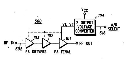
The preferred ~mbo~im~nt of the ~lCSCht invention is il-
lustrated in FIG. 1. The a~l,alatus is cG~ ,l;sed of a final
1 5 power ~mrlifier (101) and two power ~mrlifier dr;~e,s (102 -
103) cQnnecte-l to the RF input signal (502). The power ampli-
fiers (101- 103) are cornecte~l in series with the final power
plifier (101) oul~ull,i~g the ~mplified RF 6ign~l. The power
amrlifiers (101 - 103) used in the preferred eml~o~ e..t are
2 0 MHW927A man~lf~ct~lred by Motorola, Inc.
A voltage co~vel ~,or (104) is connected to the coll~ct~r
supply of each power ~mrlifier stage. The voltage cul,verlor
(104) must be an efficient supply that, in the preferred embod-
iment, is a switching power supply. The voltage cunvel ~or
2 5 (104) is conne~te~ to a voltage VcC that is 12.5 V in the pre-
felTed embo~imant The voltage convertor (104) is capable of
generating two voltages from Vcc. Which voltage is generated
is chosen by the analogl digital mode select line ( 51 6)con-
nected to the convertor (104). A logical high on this line (5 l 6)
3 0 selects the analog mode and a logical low selects the digital
mode. In the preferred Pmho~lim~nt a logical high is +5.0 V
and a logical low is 0 V. The analog mode is also referred to in
the art as the constant envelope mode and the digital mode is
referred to as the linear mode.
3 5 When the digital mode is selected, the voltage convertor
(104) supplies a voltage Vl that is close to Vcc; 12.5 V in the
-5 -
2 ~ O
preferred embodiment. This ifi the design voltage of the power
Amrlifiers (101- 103) and llows the Amrlifiers (101- 103) to
provide its ~l~siEned value of linearity at its rated power out.
Providing 12.5 V to the power ~mrlifiers (101- 103) is accom-
S rli~he-l by turning off the voltage convertor (104) and turning
on an internal pass device that allows the full Vcc to reach the
~mrlifierg with minim~l loss. The pass device is transistor,
so Vcc minus the voltage drop across the trAnsi~t~r equals the
voltage to the power Amrlifiers.
1 0 If the analog mode is selected, the voltage co.lve~ L~r
(104) is on and generates a predetel~ed voltage V2 to the
power ~mrlifiP~rs (101 - 103) that is ~i~nific~ntly less than VcC.
In the preferred emhoAim~n~" this voltage i8 8.65 V. With this
reduced supply voltage, the AC collector voltage magnitude at
1 5 the re~ ce~l power out will again be close to the DC supply
voltage as it was at the peak linear power out with the higher
supply voltage of Vcc. Efficiency in the ~n~lo~ mode, there-
fore, is still o~li~u~.
In an ideal situation, the rel~t;on~hip between the Vl
2 0 and V2 is the same as the relationship between the peak linear
mode power and the constant envelope mode power. For U.S.
Digital Cellular, the difference is 3.2 dB, thus n~lrin~ V2 3.2
dB less than Vl. For optimum perfor n~nce in a real situa-
tion, howeve~-, the difference between Vl and V2 varies from
2 5 t_e ideal due to saturation and other non-ideal P-ffects.
To illustrate the use of the dual mode power ~smplifier
apparatus of the present invention, it is first ~cfillmed that the
hybrid digital/analog radiotelephone is operating in the U.S.
Digital Cellular system. The mode selection signal (516) is
3 0 brought low to select the digital mode. This turns off the
switching power supply (104), thus allowing the 12.5 V Vcc to
be applied to the collector supply of the power ~mplifiers (101 -
103). The higher collector voltage allows the power ~mplifiers
(101 - 103) to operate linearly at their designed value of linear-
3 5 ity at their rated output power.
2~Q~!4 ~
When the radiotelephone is operating in the ~n~lo~ cel-
lular system, the mode selection signal (51 6) is high to select
the analog mode of the amplifier apparatus. The switching
power suy~ly (104) is on, generating a voltage of 8.65 V that is
S applied to the collectors of the power ~mrlifiers (101 - 103).
Since the transmitted signal is a con~t~nt envelope signal at a
reduced power out, the reduced collector voltage allows the
power ~mrlifiers (101 - 103) to operate efficiently at an AC col-
lector voltage closer to the supply voltage. The above described
1 0 met~oA of the present invention is illustrated in the flowchart
of FIG. 3.
~n~ ?r PmhoAim~nt of the present invention i8 illus-
trated in FIG. 2. This emboAimPnt is co~ ;sed of a four
stage power ~mrlifier module, such as a Motorola MHW927A
l S module. The bias for the last two stages (203) and both bias
and 8U~ for the first two stages (204) are tied together. The
collectors of the last two stages are also tied together. These
cnllecters are cQnnPcte-l to a voltage CO11V~ l)l' (204) that gen-
erates two voltages. This voltage collv~rl,or (204) the ~ame kind
of voltage oollvel~or (104) as discussed in the l,rerelled embod-
iment. The signal to be ~mrlifieA i8 coupled to the RF input
(502) and the RF output (202) is the ~mrlifieA ~gn~l, A bias
select circuit (401), illustrated in greater detail in FIG. 4, gen-
erates the bias voltage Vbb.
2 5 The Vbb selection is performed by the analogldigital se-
lect line (516). By bringing this line low to select the digital
mode, the transistor (412) is off m:~king the only voltage at the
bias of the final stage (420) of the power ~mrlifier the 0.70 V
drop across the diode (411). The power ~mrlifier is now in the
3 0 linear mode. When the analo~/digital select line (516) is high,
the tr~n~i~tor (412) is in saturation and the voltage at the final
stage (420) of the power amplifier is the 0.20 V saturation volt-
age of the transistor (412). A resistor (410) in the collector leg
of the tr~n~i~tor (412) is chosen very small, 0.1 Q in the pre-
3 5 ferred embodiment, for current limiting. The power ~mplifier
d~;vels (421 - 422) always have Vbb as the bias voltage.
WO 93/18583 PCI/US93/00225
-7 -
210f-i~L10
The embotliment of FIG. 2 will be used to illustrate the
efficiency provided by the dual mode power ~mplifier. The
bia~ connec1;on is held at 9.5 V. The collector voltage of the
last two stages was varied between the rated supply voltage of
12.5 V and a value 3.2 dB less, 8.65 V. The results of this oper-
ation are illustrated in the following table:
Digitsl Avg. PO Digital Peak PO Analog Avg. PO
Po = 37.8 dBm Po = 41.0 dBm Po = 37.8 dBm
Vcc = 12.5 V Vcc = 12.5 V Vcc = 8.65 V
ICC (A) 1.49 A 2.29 A 1.59 A
Ib (mA) 193 mA 192mA 193mA
Tlpa (%) 29.4 % 41.4 % 38.7 %
System
Ef~lciency 28.8 % N/A 33.6 %
(%)
The system effir çnry was computed assuming .2 n re-
l 0 sis~nce in a FET pass device for the digital mode and an 85%effi(~iPnt voltage convertor for the ~n~log mode. The effi~er-Gy
c~ tion for the power ~qmrlifiers is determined by the
equation:
1 5 ~P' Vb ~ 14 t Vec ~ L
where PO is the power out.
The system efficiency is computed by ~rltling the dissi-
pation of the voltage collver~ to the denomin~tor of the Tlpa
t:A~essior~- The above table shows that even with the some-
2 0 what higher convertor losses, the concept still i~ vves effi-
ciency by 4% over the digital mode.
FIG. 5 illustrates a block diagram of a typical radio
transmitter of the present invention. The actual ci~c--it,,-~ em-
bodying the functional blocks of the diagram may be mounted
2 S on one or more circuit boards and housed within a collvell-
tional radiotelephone housing. The radio transmitter re-
quires only the high efficiency dual mode power ~mplifier ap-
~al Bl,uS (104) of the present invention by providing mP~n~ to
operate the ~mplifier in either a linear mode or a non-linear
WO 93/18583 PCI/US93/00225
-8 -
2109qlO
mode. Efficient Amplification of a frequency modulated sig-
nal, and Amplifit Ation of a ~/4 DQPSK mo~ lAter1 signal is
thereby possible, while, at the same time, minimi7ing circuit
size and cost.
S The microphone (54) co~ e~ ls voice 6ignAl~ into an elec-
trical, inforTn~tion signal (56 and 58). The information signal
supplied on line (56) iS ll~li7etl when, ~imil~r to conventionSIl
cellular, radiotelephone couuu~ucations~ a frequency modu-
lated information signal i8 to be generated by the radiotele-
phone. The information signal supplied on line (58) is utilized
when a discrete, ~ncoAed signal modulated to form a cQmros-
ite modulated information signal is to be generated by the ra-
diotelephon~,
The inform~tion signal generated on line (56) iS sup-
plied to a voltage controlled osrillAtor (60) where the informa-
tion signal is comhinetl with an os~ll~ting signal of a cel l~
frequency. A frequency modulated informs~tion signal (62) is
~:nelated by the voltage controlled osr~ tor (60) to a modula-
tor (64). When the radiotelephone is to trPnsmit a frequency
2 0 modulated information ~ign~l, the modulator (64) does not al-
ter the frequency modulated information signal (62), but
rather ~passes-through" the frequency modulated information
~ign~l The oscillAtQr (60) and mo~ul~tor (64) may together
co ~l,l;se a hybrid modlllAtion apparatus (68).
2 5 The information signal (58) is supplied to a vocoder (72)
where the analog information signal is digitized and enCo~e~
accoldi~g to an enCoAing scheme, and generates a discrete,
~nco~le~ signal (76) that is supplied to the modulator (64). The
modulator (64) modulates the discrete, enco~le-l signal (76) to
3 0 form a composite, modulated information signal of a pre-de-
termined frequency.
The modulated information signal modulated accord-
ing to either a frequency mod~ tion technique or a com~osite
modlll~tion technique, is supplied to a mixer (80). The mixer
3 5 (80) mixes this signal with an offset tr~nsmission-frequency
carrier wave generated by a syn~esi7Pr (90) and supplied to
WO 93/18583 PCI'/US93/00225
g
21~10
the mixer (80). The mixer (80) mixes the modulated informa-
tion signal with the carrier wave (92). The mixer (80) then
generates a modulated information signal (96) upon a carrier
wave of a carrier frequency determined by the oscillating fre-
quency of synt~esi7ers (90 and 60).
The modulated information signal (96) is coupled to a
filter (540) that forms a r~ssb~n-l of freq-lenries centered
about, or close to, the carrier frequency of the transmitted
wave. This Slter (540) generates a Sltered signal (502), con-
1 0 tsinin~ the modulated inform~tio~ si~n-s-l, that is coupled to
the power smrlifier (500) of the present invantion. The power
smrlifier (500) smrlifies the mo~ te~ information signal to
power levels adequate for tr~n~mi~siQn through an s~n~nnsl
(506). Prior to tr~ncmission of the smrlifie~l ~ign~l, and as il-
1 5 lustrated, the smrlifie-l signal may be Sltered by another filter
(507) that may, for e~ ,le, form a portion of a dllples~r~
This Slter (507) is positioned in-line between the power ampli-
fier (500) and the snt~nn-s (506).
A processor (508) provides control ~ignslc (510, 512, 514,
2 0 and 515) to control Gl,e- a~ion of the oscill~t~r (60), the vocoder
(72), the modulator (64), and the srt~esi7er (90), respectively,
to control modulation of the information signal generated by
the microphone (54).
The processor (508) controls whether the inform~tio~
2 5 signal generated by the microphone (54) is modulated by the
oscillator (60) to form a frequency modulated information sig-
nal, or alternately, is enco~ed by the vocoder (72) acco~ g to
a discrete enCo~ing srhPme and mo-lnl~tArl by the modulator
(64) to form a composite modulated information ~
3 0 AB the modulated si~n~ls supplied to the ~mrlifier
(500), in the preferred embo~limPnt are frequency modulated
or composite modulated information sign~l~, the processor
(508) supplies analogldigital select signal (516) to the Amrlifier
(500) to cause operation of the ~mrlifier (504) in either the lin-
3 5 ear mode or the non-linear mode. The linear mode is enabled
when a ~c/4 DQPSK modulated signal is to be transmitted and
wo 93/18583 Pcr/usg3/oo225
- 10-
21~9410
the non-linear mode is enabled when an FM signal is to be
transmitted.
FIG. 5 further illustrates the radiotelephone receive
circuit for a signal transmitted to the ~ntçnn~ (506). The sig-
5 nal transmitted to the ~n~nn~ (506) is supplied to the filter
(517) which passes sign~ls of desired freql~qnrie6 to the mixer
(518). The mixer (518) lece;ves an oscill~ting signal (519) from
the synt~eEi7er (90) and generates a mi~ed signal that is sup-
plied to a ~l~mo~lulator (520). The ~çmo~ tor (520) supplies a
10 tl~mo~ te~ electrical inform~iQn signal to a spe~l~er (521).
The ~.oce3sor (508) may supply a signal (520A) to the ~lem
lator (120) to control its operation. The spe~lrer (521) collvel Is
the electrical inform~tiQn ~ien~ls into audible signP~