Note: Descriptions are shown in the official language in which they were submitted.
210956 ~
,
TITLE OF THE INVENTION
2 "Switched Capacitor Circuit Having Reduced Capacitance UnitsH
3 BACKGROUND OF THE INVENTION
4 Field of the Invention
s The present invention relates to a switched capacitor circuit which
6 operates in response to a two-phase high frequency clock signal to
7 synthesize an equivalent resistor.
8 Description of the Related Art
9 A prior art switched capacitor circuit as shown in Fig. 1 comprises
a first sampling switch S1 of single-pole-double-throw (SPDT) type
11 connected to an input terminal 100 for coupling it to a circuit node 101 in
12 response to a first phase ~1 of a two-phase high frequency clock signal13 and coupling the node 101 to ground in response to the second phase ~2
14 of the clock signa,l. A second sampling switch S2 of the SPDT type is
connected to a circuit node 103 for coupling it to ground in response to
16 phase ~1 and coupling it, in response to phase ~2, to the inverting input
17 of an operational amplifier 106, which functions as the energy supply
18 source for the switched capacitor circuit. Between the circuit nodes 101
19 and 103 is provided a variable sampling capacitor circuit SC1 comprising
a capacitor 102 with value Cs which is in shunt with a plurality of gain
21 control switches D; and sampling capacitors C; respectively connected to
22 switches D;, where i = 1, 2, .. 8. The least to most significant bits of an
23 eight-bit binary signal are applied respectively to the gain control switches24 D1 to D8 for coupling the associated capacitors in shunt with the fixed
capacitor 102 in response to a bit "1". The capacitance of each of the
26 switched capacitors C; is equal 2i x CO where CO is the capacitance unit.
27 The circuit node 103 is further connected through a transfer capacitor 104
28 to a third sampling switch S3 of the SPDT type. Third sampling switch S3
29 iS responsive to phase ~1 for coupling the transfer capacitor 104 to
3 o ground for discharging it and responsive to phase ~2 for coupling it to the
A
~ 2 ~ O 9 5 ~ ~
-
- 2 -
output terminal 107 to which the output of operational amplifier 106 is
2 connected. A feedback capacitor 105 is connected between the inverting
3 input of operational amplifier 106 and output terminal 107 to stabilize the
4 operational amplifier when the inverting input is disconnected from circuit
s node 103. Since the gain (VOUtlvin) of the switched capacitor circuit is
6 given by the ratio of the total capacitance of the variable sampling
7 capacitor circuit SCl to the capacitance Ct of transfer capacitor 104, it can8 be adjusted to one of 256 capacitance ratios (i.e., Cs!Ct, (Cs+CO)lct~
9 (Cs+2Co)/Ct, (Cs~3Co)/Ct~ .-.. , (Cs+255co)lct) in response to an 8-bit
10 gain control signal, using 255 capacitance units.
11 From the power savings standpoint of the operational amplifier
12 106 it is desirable to reduce the total number of capacitance units as well
13 as to reduce the value of the capacitance unit itself. However, the
14 precision of the capacitance ratio tends to decrease as the value of the
15 capacitance unit CO decreases due to the process limitations imposed by
16 the integrated circuit technique. Since the capacitance unit value CO
17 cannot be reduced below what is obtainable by the integrated circuit
18 technology, it is important to reduce the total number of capacitance
1 9 units.
To reduce the total number of capacitance units CO to 131 units,
21 as well as the total of the capacitances of sampling capacitors and transfer
22 capacitor to 1/64 of Fig. 1, a variable sampling capacitor circuit SC2 of
23 what is known as the ladder or T-type structure is shown in Fig. 2.
24 According to this prior art, each of the switched capacitor circuits formed
by gain control switches Dk (where k = 1, 2, 3, .. 6) includes a ser;es of
26 capacitors Ck1 and Ck3 and a capacitor Ck2 connected across the node
27 between capacitors Ckl and Ck3 and ground. All capacitors Ck1 and Ck3
28 except for C63 has unit capacitance value CO~ while capacitor C63 has
29 twice the unit capacitance value, and all capacitors Ck2 except for
3 0 capacitor C62 has a capacitance equal to (2(7-k) - 2)Co and the capacitor
-, 2 1 09 5~ 1
;_ .
C62 is of the unit value CO. The values of capacitors 102 and 104 are
2 reduced to CJ64 and Ct/64, respectively. After charging the capacitors
3 Ck1, Ck2 and Ck3, the charge stored on capacitor Ck3 is transferred to the
4 transfer capacitor 104. Since the amount of energies discharged by the
s gain control sampling capacitors is given by Vjn x Ck1 x Ck3/(Ck1 + Ck2 +
6 Ck3), each of the capacitor networks connected to switches D1 to D6 has
7 an equivalent capacitance Ck1 x Ck3/(Ck1 + Ck2 + Ck3) ranging from
8 Co/64 to Co/2. A further prior art sampling capacitor circuit SC3 which is
g known as the ~ structure reduces the total number of capacitance units CO
to 65 units as shown in Fig. 3. According to this ~-structure each of the
11 capacitor networks associated with switches Dj (where j = 1 and 2) is
12 formed by a series of unit-value capacitors Cj1, Cj3, Cj5 and grounded
13 capacitors Cj2 and Cj4 respectively coupled to the node between
14 capacitors Cj1 and Cj3 and the node between Cj3 and Cj5. The values of
the grounded capacitors C12 and C14 are 3Co and 11 CO~ respectively,
16 and those of the grounded capacitors C22 and C24 are CO and 9CO~
17 respectively. The quantity of the charges transferred from the gain
18 control sampling capacitors is given by Vin x Cj1 x Cj3 x Cjs/{(C;1 + Cj2)(Cj3
19 + Cj4 + Cjs) + Cj3(Cj4 + C;s)}. The equivalent capacitances of the
capacitor networks with switches D1 and D2 are equal to Co/64 and
21 Co/32, respectively.
22 However, there is still a need to decrease the number of
23 capacitance units for each of the T- and ~I-type of sampling capacitor
2 4 networks.
SUMMARY OF THE INVENTION
2 6 It is therefore an object of the present invention to provide a
27 switched capacitor circuit having a smalJer number of capacitance units.
28 According to a first aspect of the present invention, there is
29 provided a switched capacitor circuit which comprises a first capacitor
3 0 connected between first and second nodes, a second capacitor connected
~. ,,
~109561
- 4 -
between the first node and a third node, and a third capacitor connected
2 between the third node (M) and a reference potential. A plurality of m
3 parallel circuits are connected between the third node and the second
4 node. Each of the m parallel circuits includes a fourth capacitor and a
5 switch for coupling the fourth capacitor to the reference potential or to the
6 second node depending on a corresponding one of m bits of an N-bit
7 gain control signal, where m is an integer smaller than N. (N - m) parallel
circuits are connected between the first and second nodes. Each of the (N
9 - m) parallel circuits includes a fifth capacitor and a switch for charging the
10 fifth capacitor depending on one of (N - m) bits of the N-bit gain control
11 signal. A first sampling switch is provided for applying an input signal of
12 the switched capacitor circuit to the first node in response to a first phase13 of a two-phase high frequency clock signal and coupling the first node to
14 the reference potential in response to a second phase of the two-phase
high frequency clock signal. A second sampling switch provides charging
16 of a sixth capacitor, which is connected to the second node, in response
17 to the first phase of the clock signal and discharges stored energy from
18 the sixth capacitor to an output terminal of the switched capacitor circuit in
19 response to the second phase of the clock signal.
According to a second aspect of the present invention, there is
21 switched capacitor circuit comprising a first capacitor connected between
22 a first node and a second node. Second and third capacitors are
23 connected in series between the first node and a third node. A fourth
24 capacitor is connected across a node between the second and third
25 capacitors and a reference potential and a fifth capacitor is connected
26 between the third node and the reference potential. A plurality of m
27 parallel circuits are connected between the third node and the second
2~ node, each of the m parallel circuits including a sixth capacitor and a
2 9 switch for coupling the sixth capacitor to the reference potential or to the30 second node depending on a corresponding one of m bits of an N-bit
i
,
~ 2 1 o Q s ~ 11
gain control signal, where m is an integer smaller than N. (N - m) parallel
2 circuits are connected between the first and second nodes, each of the (N
3 - m) parallel circuits including a seventh capacitor and a switch for
4 charging the seventh capacitor depending on a corresponding one of (N
s - m) bits of the N-bit gain control signal. A first sampling switch applies
6 the input signal of the switched capacitor circuit to the first node in
7 response to a first phase of a two-phase high frequency clock signal and
8 coupling the first node to the reference potential in response to a second
g phase of the two-phase high frequency clock signal. A second sampling
switch provides charging of an eighth capacitor, which is connected to
11 the second node, in response to the first phase of the clock signal and
12 discharges stored energy from the eighth capacitor to an output terminal
13 of the switched capacitor circuit in response to the second phase of the
4 clock signal.
BRIEF DESCRIPTION OF THE C)RAWINGS
16 The present invention will be described in further detail with reference to
17 the accompanying drawings, in which:
18 Fig. 1 is a circuit diagram of a first prior art switched capacitor
1 9 circuit;
Fig. 2 is a circuit diagram of a second prior art switched capacitor
21 circuit of T-type structure;
2 2 Fig. 3 is a circuit diagram of a third prior art switched capacitor
2 3 circuit of 7~-type structure;
24 Fig. 4 is a circuit diagram of a switched capacitor circuit according
to a first embodiment of the present invention; and
2 6 Fig. 5 is a circuit diagram of a switched capacitor circuit according
27 to a second embodiment of the present invention.
28 DETAILED DESCRIPTION
29 In order to reduce the number of unit capacitances CO of the T-
3 o type sampling capacitor circuit, a first embodiment of the present
A
~ ~90g~0~
~, , .
- 6 -
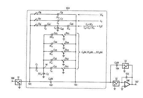
invention is shown in Fig. 4. The sampling capacitor circuit SC4 of this
2 embodiment comprises a unit-value capacitor Cl connected between the
3 node 101 and a node M and a capacitor C2 with a value of 32Co
4 connected between node M and ground, which serves a reference
5 potential. Between the circuit nodes M and 103 is connected a plurality of
6 parallel circuits each including a capacitor Cvm connected in series with a
7 single-pole-double-throw (SPDT) switch DVm~ where m = 1, 2,.... 5, and
8 the value of each capacitor Cvm is equal to 2(m-1)Co. The least significant
9 bit to the fifth significant bit of an 8 bit gain control signal are applied
10 respectively to SPDT switches DV1 to DVs. Each of the SPDT switches
1 1 DVm is responsive to a bit "1 " for coupling the associated capacitor CVm
12 to the node 103 and responsive to a llo" for coupling that capacitor to
1 3 ground.
14 When switches Sl, S2 and S3 are changed to position Na" in
15 response to the phase ~1 of a two-phase high frequency clock, a
16 charging current is supplied from terminal 100 and all capacitors CVm are
17 charged regardless of the positions of their associated switches DVm to
18 develop a voltage VM at node M. More specifically, those of capacitors
19 CVm which are coupled to ground by the corresponding switches DVm
20 (to which a bit "0" is applied) allow the charging currents to find their
21 paths to ground through such bit-0-applied switches, and the other
22 capacitors which are coupled to node 103 by the associated switches
2 3 DVm (to which a bit "1 " is applied) allow the charging currents to find their
24 paths through switch S2. Therefore, the node voltage VM, which is given
below, is precisely proportional to the voltage Vjn at input terminal 100,
26 regardless of the operating states of switches DV1 to Dvs:
VM = C15 Vin (1)
Cl + C2 + ~CVm
27 m=l
28 When switches 51, S2 and S3 are changed to position "b" in
r~ Z10956
~ 7 ~
response to the phase ~2 of the two-phase clock, those of the sampling
2 capacitors which are coupled to node 103 are brought into a series
3 connection by switch S3 to the transfer capacitor 104. The amount of
4 energies discharged by the gain control sampling capacitors Cv1 ~ Cvs is
5 given by:
M
Q = VM ~, CVm (2)
6 m=l
7 where M is the total number of capacitors Cvm which are connected to
8 node 103. Therefore, the equivalent capacitance ratio R is expressed by:
M M
Cl ~, CVm ~ CVm
R= ~1 = ~1 (3)
Cl + C2 + ~, Cvm 64
9 rrF1
It is seen that if each one of the capacitors Cv1 ~ Cv5 is coupled
11 exclusively to node 103, a capacitance value Co/64, 2Co/64, 4Co/64,
12 8Co/64 or 1 6Co/64 is brought into shunt with the fixed sampling capacitor
13 102. Therefore, a capacitance value ranging from a minimum of Co/64 to
14 a maximum of 31 Co/64 with an increment of Co/64 can be provided by a
15 combination of the least significant bit to the fifth significant bit of the 8-bit
16 gain control signal.
17 The sampling capacitor circuit SC4 of this invention includes the
18 switches D6 to D8 and their associated capacitors in the same manner as
19 shown in Figs. 2 and 3. Since the switches D6 to D8 are respectively
20 responsive to the sixth to the most significant bits of the 8-bit gain control
21 signal, the application of a bit Illn to switch D6 brings a capacitance Co/2
2 2 (= 32Co/64) in shunt with the fixed sampling capacitor 102 as the next
23 value to the maximum value of 31 Co/64 which is provided if all capacitors
24 Cv1 to Cv5 are coupled to node 103. In like manner, the operation of
25 switches D7 and D8 brings equivalent capacitances C0 and 2Co in shunt
2 6 with the fixed sampling capacitor 102.
.A
~ 2 ~ ~9 56 ~
- 8 -
It follows that a maximum of 256 capacitance ratios can be
2 provided by a combination of any of switches DVl~Dvs~ D6 to D8 using
3 71 unit-value capacitors, representing a reduction of 60 capacitance units
4 in comparison with the prior art T-type sampling capacitor circuit of Fig. 2.
s A second embodiment of the present invention is shown in Fig. 5.6 This embodiment is an improvement over the prior art 7~-type sampling
7 capacitor circuit of Fig. 3. The sampling capacitor circuit SC5 of this
8 embodiment includes the same capacitor networks formed by the gain
9 control switches D4 to D8 and their associated capacitors C41-C43,
C51~Cs3, C61~C63~ C7 and Cs as used in the prior art of Fig. 3. The
1 1 fourth significant bit to the most significant bit of an 8 bit gain control
12 signal are applied respectively to SPDT switches D4 to D8.
13 The sampling capacitor circuit SC5 includes a series of unit-value
14 (CO) capacitors C1 and C3 between circuit nodes 101 and M', a capacitor
C2 with value 3Co connected across the node between capacitors Cl and
16 C3 and ground, and a capacitor C4 with value SCO connected between
17 the node M' and ground. Between the circuit nodes M' and 103 is
18 connected a plurality of parallel circuits each including a capacitor CVm
19 connected in series with a single-pole-double-throw (SPDT) switch DVm,
20 where m = 1, 2 and 3, and the value of each capacitor CVm is egual to
2 1 2(m-1 )CO. The least significant bit to the third significant bit of the 8 bit
22 gain control signal are applied respectively to SPDT switches DV1 to Dv3.
23 Similar to the first embodiment, each of the SPDT switches DVm is
24 responsive to a bit "1 " for coupling the associated capacitor CVm to the
node 103 and responsive to a llO" for coupling that capacitor to ground.
26 When switches S1, S2 and S3 are changed to position "a" in
27 response to the phase ~1 of a two-phase high frequency clock, a
28 charging current is supplied from terminal 100 and capacitors CV1 to Cv3
29 are charged regardless of the positions of their associated switches to
3 0 develop a voltage VIM at node M' which is given by:
,~
~ 210~56 ~
g
V~M = C1 . C3 Vin (4)
(Cl + C2)(C3 + C4 + ~ cvm )+ C3(C4 + ~CVm ) +
m=l m=l
2 When switches Sl, S2 and S3 are changed to position "b" in
3 response to phase ~2, those of the sampling capacitors which are
4 coupled to node 103 are brought into a series connection by switch S3 to
s the transfer capacitor 104. The amount of charges transferred from the
6 gain control sampling capacitors Cvl ~ Cv3 is given by:
M
Q=V~M ~,CVm
7 m=l
8 Therefore, the equivalent capacitance ratio R is expressed by:
M
C1 C3 ~CVm
R = 3 3
(Cl +C2)(C3 +C4 + ~, Cvm)+c3(c4 + ~,Cvm)
9 n~l m=l
M
~ CVm (6)
64
11 If each one of the capacitors Cv1 ~ Cv3 is coupled exclusively to
12 node 103, an equivalent capacitance value Co/64, 2Co/64, or 4Co/64 is
13 brought into shunt with the fixed sampling capacitor 102. Therefore, a
14 capacitance value ranging from a minimum of Co/64 to a maximum of
15 7Co/64 can be provided by a combination of the least significant bit to the
16 third significant bit of the 8-bit gain control signal. The capacitors
17 associated with the switches D4 to D8 add an equivalent capacitance
18 ranging from Co/8 to 2Co. to the range of values provided by capacitors
19 CV1 to Cv3. The total number of capacitance units is reduced to 36,
20 representing a reduction of 29 units in comparison with the prior art ~-
2 1 type sampling capacitor circuit of Fig. 3.
" A