Note: Descriptions are shown in the official language in which they were submitted.
a
L~ ILl~JTIAL ~ATCHING INVERTER
AND RANDOM ACCESS MEMORY USING SAME
Field ofthe Invention ~ ~-
This invention relates to semicon~otor
memory devices and more particularly to high speed,
high density, low power random Access memories.
U&cbg,uund of the Invention
Read/write memories, al80 rsferred to as
Random ~ces~ Memories (RAM) are widely used to store
.Gy~ams and data for microprocessors and other
ele~L.onic dQvices. The availability of high speed,
high density and low power RAM dRvic-s has played a
crucial rol- ln the price reduction of personal
computers and in the integration o~ computer technology
into consua-r ele~ ..ic devices.
A typical RAM includes a large number of
memory cell~ arranged in an array of rows and columns.
Each memory cell is typically capable o~ storing
therein a binary digit, i.e. a binary ONE or a binary
ZERO. Each row Or the memory cell array is typically
co~e~ed to a word line and each column o~ the memory
cell array is typically co~nected to a pair of bit
lines. Read and write operation~ are per~ormed on an
individual cell in the memory by addLrc~n~ th~
appropriate row of the array using the word lines and
addressing the appl~riate cell in the address-d row
.~ ~
: ~'
~ :
~1~9'~a
--2--
using the bit lines. Depending upon the siqnals
applied to the bit lines, a write operation may be
performed for storing binary data in the RAM or a read
operation may be performed for accessing binary data
which is stored in the RAM. When read and write
operations are not being performed, the RAM is
typically placed in an idle operation for maintaining
the binary data stored therein.
RAMs are typically divided into two general
classes, ~ep~n~i ng upon the need to refresh the data
stored in the RAM during the idle state. In
particular, in a Dynamic RAnd~ Access Memory (DRAM),
the data stored in the memory is lost unless the memory
is periodically refreshed during the idle operation.
In contrast, in a Static ~And~' Acces~ Memory (SRAM)
there is no need to refresh the data during an idle
operation, hecA-~e the data stored therein is
maintAin~ a~ long as electrical power is supplied to
the SRAM. In the present state of the art, it is
generally possible to fabricate higher density DRAM
arrays than SRAM arrays because the individual memory
cells of a DRAM include fewer transistors than the
individual cells of an SRAM. However, SRAMs tend to
operate at higher ~ee~7~ than DRA~s, because there is
no need to refresh the data stored therein.
Accordingly, both SRAMs and DRAMs are typically used in
computer system~, with the SRAMs being used for high
spe-d memory (often referred to a~ "cache" memory),
while the DRAM is typically u~ed for lower speed, lower
cost mass memory.
Three general design criteria govern the
performance of random ~sce~s memories. They are
density, speed and power dissipation. Density
describes the number o~ memory cells that can be formed
on a given integrated circuit chip. In general, as
more cells are fabricated on a Very Large Scale
r
Integration (VLSI) chip, cost is reduced and speed is
increased.
The performance of random ~ccess me~ories is
also limited by the power consumption thereof. As
power consumption increases, more sophisticated
packaging is necessAry to allow the integrated circuit
to dissipate the hiqh power. Moreover, high power
circuits require eYpencive power 8uppl ies, and limit
applicability to portable or battery powered devices.
lo Finally, speed i8 also an important
consideration in the operation of a random ~ccess
memory because the time it ~akes to reliably access
data from the memory and write data $nto the memory is
an important parameter in the overall system speed. It
- 15 will be understood by those having skill in the art
that the parameters of speed, density and power
dissipation are generally interrelated, with
improvements in one area generally requiring tradeoffs
in one or more of the other areas.
In designing high density, high speed, low
power random --~e~ memories, two general de~iqn areas
may be pursued. The first is the desiqn of the memory
cell itself. For example, in a static random acce~s
memory, improved memory cell designs can permit high
speed memory operations at low power consumption. one
~uch imp~ design is described in C3~ ng
application Serial No. 07/619,101 entitled St~t~C
~ndo~ ~ce~ Memory (SRAM) ~nclud~ng Ferm~ ~hre~hold
Fleld ~ect T~ans~stors, by the p.~e~~ inventor
Albert W. Vinal and assigned to the assignee of the
present invention. A high density, high speed, low
power SRAN cell is described.
A second ma~or area in designing a high
speed, high density, lower power random -ccess memory ~-
is the design of the supporting circuits which allow
read~ng of data into, writing of data fro~, and
operational cGn~rol of, the rando~ ~cce~s memory array. -~
_4_ ~ 3 ~
These circuits for reading, writing and controlling the
operation of the RAM cell array are often critical
limitations in the design of a high speed, high
density, Iow power random access memory.
One particular criticality in the design of
random access memory is the sense circuitry which is
used to detect a binary ONE or binary ZERO ~rom one or
more cells in the random ac~e~-- memory during a read
operation. Known sensing designs are 810w, power
lo hun~l~, and have CQn~ -~ a diDproportion~te A ~ of
chip ~real estate~ (area). In particular, a linear
analog sense amplifier is typically used to amplify the
signal from a selected cell in the memory in order to
detect a binary ONE or binary ZE~O, which is typically
L~.e~cnted by a particular voltage level at the G~
of a selected cell.
- In order to properly sense one of two voltage
levels at the ou~y~L of a particular cell, linear
analog sense amplifiers typically require a reference
or bias voltage, midway b~eel. the two voltage levels.
See for example U.S. Patent 4,914,634 to Akrout et al.
entitled Reference Voltage Gener~tor for CMOS Nemories.
Unfortunately, reference voltage generating circuits
typically consume relatively large amounts of power on
the integrated circuit and also taXe up critical chip
area.
Linear anal'og sense amplifiers have also
L~ r~lred 9~ -1 ~ z~tion or the bit lines prior to
sensing, in order to ~ en~ an imk~l~nce in the bit
line~ from producing false data values. See for
example U.S. Patent 4,893,278 to Ito entitlsd
Semlconductor Hemory Devtco Includ~ng '
Prechar~e/~ z~t~on C~rcu~try For The Complementary
D~ta L~nes. Unfortunately, the need for equalization
adds to the corplexity o~ the circuitry on the merory.
Equalization also generally requires balanced '~
tran ~-~nrf ~n thQ ~ ~r~ ~enory, tb-_~b~ r-qu~r~ng ;~
D
b ~
tighter transistor tolerances and lowering the yield of
the integrated circuit devices.
High gain, high speed linear sense amplifiers
have reduced tolerance for imbalance, thereby
decreasing the numh~r of cells that can be coupled to
the sense amplifier and further limiting the density of
the memory array. The linear sense amplifier also
limits the speed of the memory because linear ~ense
amplifiers are limited by a given gain-bandwidth
product, so that the higher the gain required, the
slower-the speed of the linear sense amplifier and vice
versa.
Since linear sense amplifiers consume high
power, many memory designs deactivate the sense
amplifiers when a read operation is not being
performed. Unfortunately, deactivation reduces the
speed of the memory device because the sense amplifiers
must be reactivated prior to a read operation.
Finally, at some point during the linear
amplification of a read signal, the linearly amplified
signal must be nonlinearly converted into a binary ONE ~:
or ZERO. Accordingly, the output of a sense amplifier
i9 typically coupled to a latch, to thereby produce one
or the other binary state. See for example U.S. Patent
4,843,264 to Galbraith entitled Dynamic Sense Amplifier
For C~OS Static RAM, and U.S. Patent 4,831,287 to Golab
entitled Latching Sense Amplifier. Unfortunately,
sense amplifiers which include a combination of a
linear analog sense amplifier and a nonlinear latch are
complicated and are difficult to accurately control for
high speed operation.
It is known that the threshold voltage of a -~
CMOS inverter can be adjusted by varying the chAnne
widths and length~ of the P-ch~nnel and N-ch~nnel field
effect transistors. See U.S. Patent 5,019,725 to
Yoshino entitled Input Circuit. However, it has not
SV~S ~ T~: S~
-5/1- :
been heretofore suggested to use such inverters in a
sense circuit of a memory device.
Summarv of the Invention
It is therefore an object of the present
invention to provide an improved sense circuit for use
in a memory.
st.t~ . ET
. ,.. .~
CA 0210983~ 1998-08-06
It is another object of the invention to provide a
sensing circuit which is capable of sensing binary data
at high speed and with low power dissipation.
It is yet another object of the invention to provide
a high speed, low power random access memory design.
These and other objects are provided according to
the present invention by a Differential Latching Inverter
(DLI) which is responsive to the voltage on a pair of
differential inputs thereto. The Differential Latching
Inverter (DLI) may be connected to a pair of bit lines in
a memory array, for sensing the binary state of a
selected memory cell. When one of the input signals to
the DLI rise above a predetermined threshold, the DLI is
responsive to a small differential component between the
signals applied thereto to rapidly latch the output of
the inverter to one logical state or another. For
example, in a memory using five volt and ground reference
voltages, when an input signal to the DLI is above one
volt, and an input differential of at least two
millivolts is present between the input signals, the DLI
rapidly latches up to a first or a second logical value
depending upon which of the inputs has the higher input
differential.
The Differential Latching Inverter of the present
invention may be implemented using a minimal number of
field effect transistors, as described below, and does
not require the generation of a separate reference
voltage or require high gain analog linear sense
amplifiers for operation. Accordingly, high speed, low
power, high density sensing of signals stored in a random
access memory is provided.
A basic design of a Differential Latching Inverter
of the present invention includes a pair of
complementary field effect transistor inverters, each
3 ~
--7--
; of which is connected between ~irst and second
reference voltages, typically the power supply voltaqe
VDD and ~lound, with each inverter including an input
and an ouLyu~-. According to the invention, the FET~ of
each of the first and secon~ complementary inverters
are designed to produce an inverter transfer function
which is s~ewed toward one o~ the first or ~econ~
reference voltages. In other words, the inverters do
not produce a symmetrical inverter transfer function
relative to the first and secon~ reference voltages.
Rather-, the transfer function is skewed toward one of
the reference voltages. In a preferred embodiment, the
voltage transfer function is skewed towards ground by a
factor of 2~ less than a symmetrical inverter, 80 that
a voltage threshold of about one volt causes the
inverter to rapidly change state, upon sensing a
voltage difrerential of about two millivolts.
The ~rst and secQn~ skewed inverters of the
present invention are cross coupled by connecting the
input of the first inverter to the ~uLyu~ 0~ the s~cQn~
inverter and the input of the ~eCon~ inverter to the
ouLyuL of the first inverter, to thereby create a
latch. A ~irst bit line is connected to the input of
the Sirst inverter and a ~e ~Qn~ bit line is cenneqted
to the input o~ the ~ec--' inverter.
The Dif~erential Latching Inverter (DLI) of
the y~qent invention exhibit~ three states. When one ~ '~
or the other input to the DLI rises above the threshold
voltage and an input dif~erential of two millivolts or
greater is found beL~een the two bit line input~, the
DLI latches to a binary ONE or binary ZERO state. In a
third or reset state, in which the bit line inputs
thereto are both below the DLI's threshold voltage,
both ou~Ls o~ the DLI are ZERO. No DC power i8
dissipated by the DLI in either o~ i~s three stable
states, and minimal power i~ dis~ipated by the DLI when
it switches ~rom one ~tate to another.
~' :
.. . ..
~............ . . : ~
-8- ~ 3 3
The skewed transfer function, first and
second complementary inverters of the DLI may be
produced by controlling the dimensions of the
complementary FET transistors of the skewed inverters
5 80 that the product of the square channel saturation
current and the ratio of chAnn91 width to length of the
FETs of a first so~uctivity type i8 substantially
greater than the product of the sguare ch~nnel
saturation current and the ratio of the ~h~nnel width
to length of the FETs of the secQ~ conductivity type.
Preferably, the products of the sguare -hAnnel
saturation current and the ratio of ch~nn-l width to
length differ by a factor of ten.
In a particular embodiment of the DLI, a pair
of pull-up FETs may also be provided, with the
cor.L~olled ele~L~ s (source and drain) of a first
pull up FET being co-n-cted between the first reference ~-
voltage and the o~yu~ of the first complementary FET
inverter, and the con~,olled electrodes of a secn-d
pull-up FET being cor.e~ed between the first reference
voltage and the o,_~yu~ of the secQn~ complementary FET
inverter. The con~.olling ele~ ode (gate) of the
fir~t pull-up FET is c~r.-.~_Led to the ou~u~ of the
SQCQ11~ complementary FET inverter and the co.l~olling
electrode of the secon~ pull-up FET is csn~_Led to the
ou~yu~ Or the first complementary FET inverter. These
cros~ coupled pull-up FETs increase the latching ~peed
of the DLI.
The ou~y~L of the first and Fecon~
complementary inverters may bce coupled to a third and a
fourth complementary FET inverter, ~e~e~-ively. The
third and fourth inverters produce an inverter voltage
transfer function which is symmetrical betJ -n the
first and SeCQn~ rererence voltages. The o~ s of
the differential latching inverter are the o~u~g of
the third and fourth complementary FET inverters.
. . . . . . . . . . . . . . . , , , , ~ . , , . . . . . . , . . . . . ~ . . . . . .
~ .. , .. ~ ; - .. ,, ~, .
9 ~ a
The DLI may also include a second pull up
circuit, which is connected to the ou~u~s of the first
and second skewed transfer function inverters, for
rapidly pulling the outputs of the ~irst and seco~
inverters to the first reference voltage (Vdd), and
thereby pulling the outputs of the third and fourth
~y --rical transfer function inverters to the secon~
reference voltage (~.~u..d) in r~spo~e to an ~nput
signal applied thereto. The input signal is applied
immediately upon a s~l~cegsful data read, or i~mediately
upon varification of a sllccec~ful data write, to
rapidly bring the DLI to the third (reset) state and
prepare the DLI for a next read or write operation.
External clock timing is not required. Rather, the
reset set is initiated internally, upon completion of a
read or write operation. ~
The Differential Latçhing Inverter of the ~ -
pL. rnnt invention may be used in a high speed, high
density, low power random Acce~ memory archite~u.e as
follows. An array of memory cells is arranged in a
plurality of rows and columns, with a word line
connscted to each row and a pair o~ primary bit lines ;~
con~ ed to each column. Signal bit lines are ~-~
provided, or~hog~n~l to the primary bit lines, and a
~Y~e~ive pair of signal bit lines is co~nected to at
least one L2 ~e ~ive pair o~ the primary bit lines at
one ~nd o~ the primary bit lines. A DLI is c ~ e~ed
~t~ -- each pair o~ aignal bit lines.
The primary bit lines are coupled to a first
reference voltage, typically power supply voltage V~,
during the idle operation, and a selected one of the
pri~ary bit line pair3 is ~e~ led ~rom the ~irst
reference voltage dur~ng a write operation. The signal
bit lines are coupled to a secQn~ re~erence voltage,
preferably ~,o~.d, during an idle operation and are
~ecourled from the secon~ voltage during a read or
write operation. The primary bit lines and the signal
,.;.. . -
h,~ 3
--10--
bit lines are coupled together during read and write
operations and decoupled from one another during an
idle operation.
The primary bit lines may be coupled to the
f~rst reference voltage using a first coupling means.
The signal bit lines may be coupled to a seco~
reference voltage using a secon~ coupling mean~, and
the primary bit line~ and the signal bit lines may be
coupled together using a third coupling mean~. In one
- ~o~iment~ the third coupling means i9 located at the
one end of the primary bit lines, ad~acent the signal -~
hit lines, and the first coupling means is located at
the opposite end of the primary bit lines, distant ~rom
the signal bit lines.
It has been found, according to the ~-
invention, that impro~ed results are obt~ine~ when both
the first and the third coupling means are located at
the one end of the primary bit lines, ad~acent the
signal bit lines. The voltage drop due to the ~;
resistance o~ the primary bit lines is eliminated, and
the speed of the random aCCe~ff memory i5 increased. In
this configuration, the primary bit lines operate as
unterminat-d transmission lines. F~hack be~2u the
signal bit line~ and either the first coupling means or
the eecon~ coupling means, or both, may also be
provided to ~urther increase ~peed.
Accordingly, during an idle operation each of
the primary bit line pairs i9 re~e~...ced to VDD and each
o~ the slgnAI bit line pairs i8 referenced to ~OUnd- ~:
; 30 All o~ the DLIs are in their third or reset state. In ~ -~
order to read, the signal bit lines are dlFc~urled from
the sec r n~ voltage reference BOu~ o~.d) and tho
primary kit lines remain coupled to the ~irst voltage
re~erence sou,ce (VDD). A word ~ec~ ~r selects a given
row. A bit ~eco~er couples a primary bit line pair in
a selected column to its A~ociAted signal bit line
pair. The amount of voltage delivered to ono bit line
--ll--
or the other of the selected primary bit line pair
drops more rapidly than the other due to the current
cond~cted by one of the memory cell pass transistors,
as controlled by the state of the selected memory cell
S being read. This current di~ferential translates to a
voltage differential on one or the other Or the signal
bit lines of the associated signal bit line pair. When
the voltage differential on one of the signal bit lines
~cee~lR the DLI's threshold voltage, the DLI will
rapidly latch into one or the other state dep~nAi~g on
the signal bit line which had the higher voltage.
Accordinqly, high speed sensing of data read from a
random ~ccess memory is provided with minimal -
~uypoL~ing circuitry.
The ou~yu~s of all of the DLIs may be
directly connscted to a pair of OR gates, with the -~
o~yut of one OR gate signifying that a logical ONE has
been read and the o~u~ of the seconA OR gate
' signifying that a logical ZERO has been read.
Connection of all of the DLIs to a ~ingle OR gate for
~ -ad~ng is possible because all o~ tho DLIs which are
not being read are in their third or reset state with
both o~Lyu~6 thereof at ~LOUnd potential. The vuLyu~
of tho ~ctivated DLI may b- pl~ceA in a read register
2S and provided a8 the memory Ou-~u~. Once a DLI has been
latched and the data has been read, the memory is
rapidly re~tored to the idle state by pulling the
active DLI back to its idle state. The signal bit
lln-~ are ,~ rled to ~L-vu.. d, the primary bit lines ~ -
remain coupled to VDD and the signal bit lines and
primary bit lines are dq~rled ~rom ono another.
Accordingly, a sel~-timing operation is provided.
In a write operation, a word ~P~der selects
a given row, a selected pair o~ primary bit lines is
dqco~rled from VDD by a decode~A. write gate, and one
selected primary bit line pair i5 coupled to an
applv~riate signal bit line pair. One of the signal
. CA 0210983~ 1998-08-06
bit lines is clamped at a LOW level thereby forcing the
associated primary bit line towards ground. This forces
one side of the selected memory cell towards ground while
holding the other side to greater than VDD/21 thereby
storing data into the selected RAM cell. At the same
time, the data written into the selected memory cell is
also read by the associated DLI as described above. The
successful read causes the memory to be reset in its idle
state as described above.
According to another aspect of the present invention
a circuit may be used with the DLI and memory
architecture described above, to detect an address change
at the memory input and initiate a read or write
operation. The address change detection system uses a
transition detection delay unit for each address bit of
the memory. The transition delay unit is responsive to a
change in its associated address bit to provide a clock
output pulse of predetermined duration.
The transition detection delay unit comprises a
la~ch which is coupled to the associated address bit, and
a pair of Delay Ring Segment Buffers each coupled to a
respective output of the latch. The design and operation
of the Delay Ring Segment Buffer is described in
copending Canadian application Serial No. 2,078,778
entitled High Speed Logic and Memory Family Using Ring
Segment Buffer by the present inventor Albert W. Vinal,
assigned to the assignee of the present invention, the
disclosure of which is hereby incorporated herein by
reference. The output of the delay ring segment buffer
is provided to cascaded NAND gates to form the output of
the transition detection delay unit.
The outputs of all of the transition detection delay
units are provided to an OR gate which is preferably a
Complementary Logic Input Parallel (CLIP) OR gate, as
described in Canadian application Serial No. 2,101,559
entitled Complementary Logic Input Parallel (CLIP) Logic
Circuit Family by the present inventor
3 ~
-13-
~lbert W. Vinal and assigned to the assignee of the
present invention, the disclosure of which is
incorporated herein by referenca. The ouL~t of the
CLIP OR gate provides an indication of an address
change. Accordingly, the transition detection delay
unit uses simple circuitry to detect an address ch~e,
with less time delay than known addres~ chAnge
detection circuits. Similar transition detection is
employed to detect a chip select active transition and
a write enable transition. The 0~ 8 of these
transition detect delay units are also coupled to the
CLIP OR gate, and are also used to activate the memory
cycle.
Once a ch~nge in the address has been
detected, or a chip select or write enable signal has
been detected, internal timing of the memory may be
provided by a series of Delay Ring Segment Bu~fers.
The Delay Ring Segment Bu~fers provide the ~equired
timing signals to word and bit ~eco~ers and the DLIs as
described above. Once the data has been read, or data
has been written and verified, the timing circuitry
generates a reset signal to rapidly place the memory in
the idle state. Sel~-timlng of memory operations is
thereby provided. - ~-~
It will be understood by those having skill ~ -~
in the art that the Differential Latç~lng Inverter of
the ~r~c~ invention may be u~ied in con~unction with
other memory archite~Lu.es than described herein.
Slmilarly, the memory archite~u.a described herein may
be used with sensing circuits other than the
Differential Latching Inverter. Finally, the ~n1~?
control circuits such as the ad~LQss detection chA~,e
circuits and the timinq circuits using ring segment
buffers, may be used to control memories other than
those described herein. ~ow_~sr, it will be also be
understood by those having skill in the art that the
unique combination of the ~LI, memory archite~u~e and
14 ~~ 3 ~
supporting control circuitry described herein provides
a high density, high speed random access memory with
very low power dissipation.
s Brief Des~,iution of the D.~-.;nqs
Figure 1 illustrates a schematic circuit
diagram of a Differential Latching Inverter according
to the present invention.
Figure 2 illustrates the inverter trans~er
functions of the symmetrical inverters and the skewed
inverters o~ the Differential Latching Inverter of
Figure 1.
Figures 3A-3D illustrate timing diagrams-for
- operation of the Di~ferential Latching Inverter of -
- 15 Figure 1. '
Figures 4A and 4B, which form Figure 4 when
pl ace~ adjacent one another as indicated, illustrate a
block diagram of a random ~cess memory archite~Lule
according to the invention incorporating the
Differential Latching Inverter o~ Figure 1.
Figure 5 illu~trates a schematic circuit
diagram of read and write control circuits for a random
~cce~s memory according to the present invention.
Figure 6 illustrates a sche~atic circuit , ~'
diagram o~ a data input register for a random acces~
memory acco,rding to the ~as~rL invention.
Figure 7 illustrate~ a schematic circuit
diagram of timing control circuitry for a random ~cce~
memory according to the present invention.
Figure 8 illustrAtes a block diagram of an ~'
address ch~r,e detection circuit according to the
pl~_a;L invention.
Figure 9 illustrates a block diagram o~ an
alternative addre~s ch~nge detection circuit according
to the ~L~ ge ~ invention.
-15~
Figure 10 illustrates a timing diagram for
operation of the address change detection circuits of
Figures 8 and 9.
Figures llA and llB are truth tables to
illu~trate the operation o~ the addres~ chAng~
detection circuits of Figures 8 and 9 respectively.
Figure 12 i8 a circuit schematic diagram of
the address change detection circuitry of Figure 9.
Figure 13 i8 a timing diagram for a random
access memory according to the present invention.
Figures 14A and 14~, which form Figure 14
when piaced ad~acent one another as indicated,
illustrate a bloek diagram of an alternate random
acce~s memory architecture according to the invention,
incorporating first and third coupling means which are .
both located between the primary bit lines and the
signal bit lines.
Figures 15-19 illustrate alternate
~ embodiments o~ the ~irst and third coupling means of
Figure 14.
D~scfi~U~ of a Preferred Embodiment
The ~F~ ~ invention now will be de3eribed
more fully hereina~ter with referenee to the
aeeompanying drawings, in whieh a preferred embodiment
Or the invention i5 shown. This invention may,
~:wa~er, be mbodied in many di~erent form~ and should
not be ~ a~ limited to the embodiment set rorth
hereins rather, this embodiment is provided 80 that
this di6closure will be thorough and eomplete, and will
~ully cGnv~y the scope of the invention to those
skilled in the art. Like numbers re~er to like -~
Qlements thro~l~ho~lt.
The design and operation o~ the random aeeess
memory o~ the ~s~t invention will be deseribed by
~irst describing the Differential Latching Inverter
(DLI). The overall archite~Lu~e o~ the memory array
~ .3
-16-
including the Differential Latching Inverter will then
be de~cribed, followed by the operation o~ the memory
during idle, read and write cycles. The control
circuits for performing the read, write and idle
operations will then be described.
Dif~re,~lialLatchinglnve~er
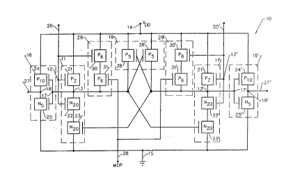
Referring now to Figure 1, a Di~ferential
Latching Inverter (DLI) according to tho present
invention will now be described. As shown in Figure 1,
DLI 10 includes a pair of cross coupled, skewed
transfer function complementary field effect transistor
inverters 11, 11~. The manner in which the skewed.
transfer function inverters are designed will be
described below. When the input signals on one of bit .
lines 20 or 20~ rise above the DLI's threshold voltage,
and a small differential signal component, for example
at least two millivolts, is present, a binary out~
latchup condition rapidly oc~, a that pro~l~ces a binary
ONE value at one of vu~put t~arminals 27, 27~ of the DLI
and a binary ZERO value at tho other one o~ v~puL
terminals 27, 27~ o~ the DLI. The binary signal state
o~ the selocted RAH cell being read is determined by
which v~yu~ terminal 27, 27' of the DLI is HIGH. ~-~
The P~ a~ inverters 11, 11~ are connscted
~t~eon a first re~erence voltage 1~ (here shown as
powor supply voltage VDD) and a ~econA reference voltage ~-
15 (here shown a9 ~ound). The input 12, 12~ o~ a
.~_,e ~ivo inverter 11, 11' i~ cQnnected to a
,e~e~ivo one of a pair of bit lines 20, 20~. As also
30 shown in Figure 1, the skewed complsmentary invertors ;~
11, 11~ are cross coupled, with the GU~U~ 13 of '
inverter 11 being csnnected to an input of inverter 11'
and the u~-~uL 13~ of inverter 1l~ boing connected to
an input of invorter 11.
It will be understood by thoso having skill
in the art that skewed complementary inverters 11, 11
.... _ . .. . .
-17-
may be formed using a pair of complementary (i.e. N-
~h~n~el and P-channel) field effect transistors, with
the inverter input being the gates of the transistors
and the sources and drains of the transistors being
serially con~ected between power supply and ground, and
the inverter output being the co~nection node between
the field effect transistors. However, a preferred
embo~ ~nt of the skewed inverters 11, 11~ i3 ag
illustrated in Figure 1. As shown, each inverter
lo comprises a first cen~uctivity (P-channsl) transistor
21, 21~ and a pair of ~econ~ cQn~llctivity (N-ch~n~el)
transistors 22, 22~ and 23, 23~, ~e~e~ively. The
cohL~olled electrodes of these transistor~ (drains and
sources) are serially co~nected between the power
supply 1~ and ~Lound 15. The gates of transistors 21
and 22 are coupled to bit line 20 and the Ou~u~ of the
inverter 13 is the connection node between p_chAnn~
transistor 21 and N-chAnn~l transistor 22. Similar
cQnnections apply to inverter 11~. In order to cross
couple the inverters, the ou~ù~ 13 of inverter 11 is
coupled to the gate of transistor 23~ and the uu~uL ~-
13~ of inverter 11~ is coupled to the gate of
transistor 23.
DLI 10 also includes an optional pair of
sym~etrical transfer function invertors 16, 16~ with
each sy~metrical inverter 16, 16~ compri~ing a pair of ;~
complementary transistors 2~, 2~ and 25, 2S',
connected ret~_~n power supply voltage 1~ and ~.Gu..d
15. The input 17, 17' of the symmetrical inverter 16,
16~ is cQ~--,r~ed to the respective o~uL 13, 13~ of
the skewQd inverter 11, 11~. The uu~u-g 18, 18~ of
the symmetrical inverter 16, 16~ ~orm the o~L~s 27, ;~
27' of the DLI. The manner ln which symmetrical
inverters 1-, 16~ are designed will be described below.
DLI 10 also includes optional pull-up circuit ~ -
19. As shown, pull-up circuit transistors 26, 26~ are
co~nected bet - power supply 1~ and the leA~e_~ive
? ~
-18-
output 13, 13' of skewed inverter 11, 11'. The gates
of pull up transistors 26, 26~ are cross-coupled to the
respective out~ut 13, 13~ of the skewed inverter 11,
Still referrlng to Figure 1, an optional
~ocon~ set of ~9, 29~ of pull-up transistors i8
provided. Each optional ~econ~ pull-up circuit 29, 29
includes a pair of transistor~ 30, 30~ and 31, 31~,
serially coupled between power supply voltage 1~ and a
respective uu-~uL 13, 13~ of the skewed inverter 11,
11~. As shown, the gate of one transistor 30, 30' is
connected to the respective bit line 20, 20~ and the
gates of the other transistors 31, 31' are coupled
together to form a memory operation (MOP) input 28.
The operation of this MOP input will be described in
detail below. Briefly, during read or write operation,
the MOP input 28 is high so that it doesn't effect
operation of the DLI. ucw-.er~ at the conclusion of a
read or write operation, the MOP input 28 is brought
LOW to turn on the pull-up circuit 29, 29', and rapidly
force nodes 13, 13~ to VDD~ thereby forcing DLI u~L~uts
27, 27~ to ~LV~d.
Rererring now to Figure 2, the inverter
transfer functions of symmetrical inverters 16, 16~ and
sXewed inverters 11, 11~ are shown. As shown, the
ouLyu~ voltages (at nodes 13, 13~) of the ~k~u~d
inverter~ 11, 11' are skewed towards the secon~
refelencc potential 15 (i.e. ~Lound) relative to the
input voltages thereof (at nodes 12, 12'). In
particular, for reference voltage~ of 5 volts and
o~nl, the o~u~ voltages of ~eue1 inverter~
rapidly ~hang8 state at an input voltage of about one
volt. Stated di~ferently, the o~ L voltage iB ~ wed
by a factor of 2~ less than a symmetrical inverter.
This conLL~sts with the inverter transfer function of
the symmetrical inverters 1~, 16~, the ou~- voltages
o~ which (at nodes 18, 18'~ ch~nge state symmetrically
,. ., , : ., . - ~ . .. . .
19 -
about an input voltage (at nodes 17, 17') approximately
midway between the first reference voltage 1~ and the
second reference voltage lS. For five volt and ground
reference voltages, the symmetrical inverters switch
state at about 2.5 volts.
Left hand skewing of inverters 11, 11~
~a~ lishes two primary results. First, it allows DLI
10 to sense a voltage differential on bit lines 20, 20
immediately after one of the bit line3 rises above the
lo noise level. Se~sing not need to wait until the bit
lines rise to half the power supply voltage. SeconA,
it causes the slope ~voltage ga~n) of the transfer
function at the skewed switching point to be much
higher than it i~ at the midway point. Compare the
lS slopes of the two curves of Figure 2. Rapid latchup i~.
thereby provided.
Left hand skewing of the voltage transfer
function of inverters 11, 11~ is accomplished by making
the product of the N-chAnnel transistor (22, 22', 23,
23') maximum square chAnnel saturation current (I~satN)
and the ~annel width-to-length ratio of the N-channe
transistors substantially larger than the p~u~ of
the P-rha~lel square chA~-.fl saturation ~rel-t ~I~satP)
and the çhannel width-to-length ratio o~ the P-channe
transistors 21-21~. It will be understood by those
h_ving skill in the art that the sguare chAnnsl
saturation ~uLL~n~ is the maximum current which can be
proA~ceA by a ch~nnsl having equal length and width.
The square channel saturation ~LLen~ is pLupG~tional
to the value o~ the carrler mobility in the Le~ye~ive
transistor; i.e. the electron mobility in the N-cha~ne
transistor and the hole ~obility in the P-chAnnel
transistor. Since the ~hannel lengths of all FET
transistor~ in a typical integrated circuit are
generally ~ade equal, above the relationship ~ay be
generally L~pr~ented as:
(I~satN)(Z~)>>(I~satP)(Zp)
a
-20-
Preferably the product of saturation current and
channel width of the N-channel devices is made ten
times greater than that of the P-channel devices. For
silicon devices having egual c~nnel lengths, the
relative chAnnel widths of the P-ch~nne1 device~ 21,
21' and the N-~h~nnel devicea 22, 22', 23, 23~ are
shown in Figure 1 inside the respective transistors.
These ch~nnel widths can be scaled to any desired
groundrules.
As also shown in Fiqure 2, inverter 16, 16'
has a symmetrical voltage transfer function. This is
obtained by making the product of the square ~hAnnel
saturation current and the width-to-length ratio of the
P-chAnnel transistors substantially equal to that of
the N_~hA~ne1 transistors. Since ror silicon, the P- -
~hAnn~l tran~istor has a square ~hAnn9l saturation
current about half that of a N-~hAnne~ transistor, the
symmetrical transfer function is obt~ine~ by making the -~-
chAn~el the P-chAnnsl transi~tor twice as wide as the
N-chA~nel transistor. Tho relative dimensions are
ahown in oach transistor in Figuro 1.
Dfflerential Latchina Inverter O~ on
Operation of the Dif~erential Latching
Inverter (DLI) 10 o~ Figu~e 1 will now be described.
In general, when the input signal on ono o~ bit lines
20, 20' ri~e~ above tho DLI'~ threshold voltaqe, the
DLI uu~uL~ 27, 27' rapidly latch to l~ t ono or
tho other binary signal state. Spocirically, when one
Or tho ~ignal~ on the bit lines 20, 20~ i5 above the
threshold voltago of the DLI, and a small dirforential
signal com~or.e~,~, rOr example o~ at least two
millivolts, is y.~ecent, a binary G~yu~ latcbup
condition rapidly oc~ù.~ that pro~uces a binary ONE
signal at one o~y~ terminal 27, 27~ of the DLI and a
binary ZERO ~down) signal at the othor ~yu~ 27, 27'
of tho DLI. The binary signal ~tate Or the selected
-21-
memory cell being read is determined by which output
terminal 27, 27' of the DLI is HIGH. For example, when
o~u~ 27 goes up to VDDI a binary ONE has bsen read
from memory, and when ou~pu~ 27~ goe~ up to VDD a binary
ZERO has been read from memory.
The DLI has a third or reset state that
occurs when both o~uLs 27 and 27~ are at DOWN level
(i.e. at or near ground level). The third state is
automatically set when the bit l~nes 20, 20~ are both
lo at or near ~luul.d potential. When the DLI is not being
called-to read or write, both of the bit lines 20, 20
are placed at yLOul~d potential so that both ou-~u~
terminals 27, 27~ are at LOW ouL~uL state, i.e. at
~,ound. It will be understood by those having skill in
15 the art that substantially no DC power is dissipated by ~ -~
DLI 10 in any of the three stable states. ~inimal
power ~8 dissipated only during the switching interval;
i.e. when switching from one state to another. The
amount of power dissipa~ed is a function of the
switching fre~le~cy.
During a read operation, a selected bit line
pair is coupled to a single memory cell selected by a
word line. Once coupled together, the voltage on bit
lines 20, 20' both ramp-up from ~r~"d. ucw-~er~ the
ramp-up rate is faster on one bit line than the other
bit lins a~ a function of whether the selected memory
cell is storing a binary ONE or ZERO.
It will be recalled that the inverter
transfer function of inverters 11, 11' i~ ~kewed
towards ~uun~ potential. For example, voltage level
transfer uay occur at around one volt. Accordingly,
assume that the voltages on bit lines 20 and 20~ are
increasing from ~L~nd, but that the voltage on bit
line 20 i8 increasing from ~Loun~ at a slightly fa~ter
rate due to the binary value stored in the selected RAM
cell. When the voltage on bit line 20 eYcee~C one
volt, the o~u~ 13 of inverter 11 rapidly switches LOW
-22-
(to ground potential), forcing the o~uL 13~ to remain
HIGH (near VDD). Since output 13 is at ground
potential, the input to cross-coupled transistor 23~ is
also at ~.ound potential turning off transistor 23~ and
thereby forcing node 13~ to VDD~ Accordingly, latchup
rapidly occurs.
In summary, the DLI include~ a ~eedback mode
of operation which results in a high gain rapid
lat~hinq condition determined by the imbalance in input
Ibit line) ramp-up voltage rates. A two millivolt
difference between the input signals above threshold is
sufficient to cause the desired latchup state. The
sQnsitivity of the DLI to the RAM cell state to i~ce
a differential signal component during a read cycle is
primarily due to the heavily left hand skewed voltage -
transfer function in the inverters 11, 11'.
The first pull-up circuit 19 increases the
latchup speed o~ DLI 10. In particular, if bit line 20
first eY~ee~C threshold and the ou~ut 13 of skewed
inverter 11 is first forced to ~Loul.d, transistor 26
of pull-up circuit 19 is turned on, thereby also
rapidly bringing (or holding) node 13' to VDD. Since
node 13' is HIG~, transi~tor 26 i8 turned of~ and does
not pull node 13 up. Accordingly, pull-up circuit 19
increases the speed at which latchup O~ULS-
It will be assumed for the present that MOPinput 28 is at HIGH logic leval 80 that transistors 30,
30', 31 and 31~ are of~ and the 8eCQ~ pull-up circuits
29, 29' are not operational. SecQ~ pull-up circuits
29, 29~ are used to restore the third or reset state of
the DLI at the conclusion o~ a read or write operation,
as will b- described in detail below.
It will also be understood by those having
skill in the ~rt that symmetrical inverter 16, 16' may
be used to provide an o~yu~ 27, 27' for the DLI which
is a TRUE v~yu~ (as o~oFe~ to a COMPLEMENT u~y~) of
the se~-el signal. In other word~ th~ voltage in
3 ~
-23-
bit line 20 increases faster than 20~, the latchup will ~-
force output 27 ~IG~ and 27~ LOW. It will al90 be
understood that inverter~ 16, ~6~ should have a
symmetrical voltage transfer function so that they
latch up rapidly when output nodes 13, ~3~ of the
skewed inverters change state.
Referring now to Figures 3A-3D, the above
described operation is illustrated. Voltage wave forms
for the bit lines 20 and 20~ and the o~uL~ 27, 27~ of
the skewed inverters ~1, 11~ are ~hown. As shown in
the first time interval for Figures 3A-3D, when the
input on bit lines 20, 20~ are below about one volt,
the OU~yu~8 27, 27~ remain at ~ vu,.~. However, as
shown in the first time interval of Figure 3A, when the
voltage on bit line 20' i8 greater than about one volt
and eY~e~ the voltage on bit line 20 by about two
millivolts, line 27~ rapidly latches to S volts and the
slight rise in line 27 is immediately suppressed by the
fee~hack condition. During a data read operation
latchup o ~ù,a in about 1.65 n~nosecon~C from the start
of the word pulse, u~ing 0.8 micron ~Loundrules. The
~eco~ time interval of Figures 3A-3D illustrates the
latchup of Gu~y~L ~7 in ~yons~ to the voltage on bit
lin- 20 being higher than that o~ bit line 20'. After
~ensing o~ the stored data o ~ur~, the voltage on both
ou~ ar- rapidly bLo~gl.~ to ~,ou,.~ by operation of
the MOP input 2~ which will be described below.
Memoly Architscture Inc~ The DLI
Having described the de~ign and operation of
the DLI, a high speed, low power, high density memory
archite~ which uses the DLI will now be described.
This archite~Lu~L will be describQd relative to an
S~AM, hsw-~r it will be undQrstood by tho~e having
skill in the art that the archite~ a may al~o be used
in a DRAM.
-24~ 3 ~
Referring now to Figures 4A and 4B, which are
placed together as indicated to form ~igure 4, random
access memory (RAM) ~0 comprises an array o~ cells
~l. It will be understood by those having skill in the
5 art that RAM cells 41 may be SRAM cells or DRAM cells,
and may use cell designs well known to those having
skill in the art. As illustrated in Figure 4, RAM
cells 4l are configured in an array of m rows and n
c:olumn For example, in a 128k bit RAM, 256 rows and
10 512 columns of RA2~ cells may be used. As also shown, m
word lines ~2a-~21~ are coupled to a one-o~-m row
~lec-o~lPr 43 for Accessing one o~ word lines 42a...42m.
As also shown in Figure 4, n pairs of bit lines 44a,
44a~-4411, 44n~ are connected to the respective n rows
15 of the array. As will be described below, two sets of
bit lines are used in RAM 40, so that bit lines ~4 are
referred to as the "primary" bit lines.
Still referring to Figure 4, it may be seen
that p pairs of "signal" bit lines 45a, 45a~-45p, 45p~
20 are provided, with every p'th pair Or primary bit lines
44 being cc~ne_led to a .e~e-;Live one of the signal
bit line3 45. In the example shown herein, p3I6, i.e.
16 pairs of signal bit lines 4S, 45~ are provided, with
every 16th column being cor~nected to a respective one
25 of the bit lines. In other words, bit line pairs 441
441~ 4417~ 441J ---44~"~ 44",' are cQnnected to signal
bit lines 45~, 45~, and bit lines 441~ 441~~~~44
44~---44~12~ 44~12~ are cornected to signal bit line
pa~r 4Sp, 4Sp~. The signal bit lines are generally
30 ortho~rr~Al to the primary bit lines.
The choice of the number Or signal bit line
pairs ~l~pe~ on several ~actors. In particular, it
ha~ been ~ound that the total capacitance which loads
the primary bit line~ ~4 should be equal to or greater
35 than the tot~l capacitance lo~Atng the signal bit lines
~5. The total cApac1tance which loads the signal bit
lines 45 is primarily due to the dif~u~ion carAcitance - ;~
J
3 ~
-25-
of the coupling transistors which couple the primary
and signal bit lines, as described below. It has been
found that this lo~ing capacitance should be minimized
to achieve the maximum memory clock ra~e and mini~um
S data Ac~ess time and i8 inversely proportional to the
number of DLI 10 used to configure the system.
Finally, the relation~h1p between m (the r ~?r of
rows), n (the number of columns), and p (the number of
DLIS) will also dQ~ ' on the overall conPiguration of
the RAM 40.
Continu~ng with the description of Fiqure 4,
a DLI lOa...lOp is connected to a re~pective signal bit
line 4Sa...~5p. First, secon~ and third coupling
means, 46, 47 and 48 respectively, are used to
~electively couple the primary bit lines 44 to the
first refe.ence potential 14 (VDD), to selectively
couple the signal b$t lines 4S to the 8eCQn~ reference
potential 28 (~Lound), and to selectively couple the
primary bit lines 44 to the signal bit lines 45. In
particular, the fir~t coupling means comprises n pairs
of p-~hAnnel transis,tors 49~, ~9a'-49n, 49n' for
coupling a ,ss,e tive primary bit line 44-, 44~'...44n,
~4u~ to VDD under CVn~LO1 Of gat~ inputs 51--S1~.
S~s~n~ coupling means 47 comprises p pairs of N-chAnns
25 FET~ 52~, 52~'-52~, 52p', each of which couple~ a
e_~iVQ ~ignal bit line 4S~, 45a~-45p, 45p~ to
.vun~ ~ under c~n~lvl of gate 53. Finally, third
coupling means 48 is seen to include P-ChAnn~l
transistor~ S4a, 54a'-5~n, 54n' for coupling a primary
30 bit lin~ 44a, ~4a'-4~n, ~4n~ to a le~e~-ive si~nAl bit ~
line ~5-, 45-~-4Sp, 4S~ under control o~ gate 55a-55n. ~:
An N-chAnnel transistor 56a, S6~-56n, 56n' al80
couples a ~e~e~ive primary bit line 44a, 44~-44n,
4~' to a ,e~pe~ive signal bit line 4Sa, 45a~-4Sp,
35 45p' under con~ol of gates 57a-57n.
As will be seen from the operational
description below, the first coupling mean~ 46 couples
. .
~ .. - ~ . . . . . . . . .; . ; ..
~10~
-26-
the primary bit lines to VDD during the idle operation
and during the read operation and deceuples at least
one of the primary bit line pairs from VDD during a
write operation. The second coupling means ~7 couples
the signal bit lines to g.ound during the idle
operation and ~e~ourles the siqnal bit lines from
~ ound during a read operation and a write operation.
The third coupling means ~8 couples the primary bit
lines to the signal bit lines during a read and write
operation and ~ecol~rles the primary bit lines and
signal bit lines from one another during an idle
operation. In particular, P_C~AnnO1 tran~istor~ S~
couple the primary bit lines to the signal bit lines
during read operation and N-~hannel transistors S6
couple the primary bit lines to the signal bit lines
during a write operation.
~ .:
O~.~ion of the ll~n~o,~\ Access Memory :
The detailed operation of the random ~ccess
memory ~0 ~Figure 4) will now be described. ~The ~dle
state will first be described followed by the read
state and then the write state.
During the idle state, a LOW logic level is
provided to gates 51 of first coupling means ~6 to turn
all o~ transistors ~ on and thereby place the primary
bit line~ ~ at the power 9Upply level V~. At the same
ti~ , a HIGH iogic level is provided to input S3 to
turn on ~e~Dn~ coupling means ~7, and thereby couple
all of the signal bit lines ~5 to ~ nd. A high logic
level 18 applied to input~ SS and a low loqic level is
applied to inputs S7 to thereby turn transistors S~ and
S~ of~ and thereby ~ecourle the primary bit lines
rrom the signal bit lines ~5. Flnally, 6ince all o~
the signal bit lines ~S are at ~-o~nd, all of the DLIs
10 are in their third or idle state with all o~ the
ou~ 8 27 and ~7~ being at ~,o~d potential. No DC
power is consumed by tha circuit during the idle state.
h~ a
-27-
During a read operation, row decoder ~3
selects one of word lines 42a...42~ to access a
particular row of RAM cells 41. A logic LOW signal is
applied to input S3 to turn ~con~ coupling means ~7
of~ to thereby ~eco~rle signal blt lines ~S from
ground. Although not coupled to gLuu..d, the
capacitance of the si~nal bit lines maintains the
signal bit lines near yLound potential. A logic LOW
level i8 maintaine~ at gates 51 to thereby continue to
couple the primary bit lines to V~. A column ~ecoA~r,
not shown in Figure 4, provides a LOW logic level to a
selected one o~ inputs of 55~-S5n ~2~en~ng upon the
column to be read. This turns on the appropriate
transistor pair S4, 54~ and causes current to flow
lS bet~een the associated primary bit lines ~4, 4~, and
the signal bit lines 4S, 4S'.
It should be noted that FETs 54 are connected
as current controlled devices, the current through
which is cont,olled by their source voltage.
Accordingly, the primary bit line which is at a highsr
voltage wlll produce more current to pull up the signal
bit lines, than the primary bit line whlch i8 at a
lower voltage- Since the selectad RAM cell ~ULlen~
tries to ~i~charge one or the other side Or the primary
bit lines 44, 4~, the voltage o~ one Or the primary
bit lines drops irom V~ at a rate ~aster than the
othor, ~ e~'~ng on the state o~ the selQcted RAM cell ~;
41. C~.h~ flow~ between the sele~ted primary bit
line pair 44, 44', and the ~ignal blt~ lines 45, 45~,
causing a di~e,en~e to occur in the voltage ramp-up
rate on the signal bit line pair 45, 45'. When the
ramp-up voltage on one or the other o~ the signal bit
lines ~5, 45~ ~Ycre~ the thrs~o1~ of the DLI 20, the
u~yu~ of tho DLI i~ rapidly latched to a ONE or ZERO.
In other words, either vu-p~t 27 goea HIGH and 27~ goes
LOW or G~tyu~ 27~ goes HIGH and 27 goes LOW.
~:;
-28-
As described in detail below, the outputs 27
of all ot the DLIs may be gated (ORed) together because
I all of the DLIs which are not active are in their third
¦ state. Accordingly, t~e ou~ of the activated DLI
may be placed in a read register and provided as the
chip output, as described in detail below.
Once a DLI has been latched and the data has
been read, the RAM is rapidly restored to the idle
state by activating the MOP input 28 ~Figure 1) with a
log~c LGW signal, to immediately pull the DLI back to
its idle state. At ~he same time, once the data has
been read, a HIGH signal is applied to input 53 to
thereby reactivate s9cond coupling means to ~e~u~.. the
signal bit lines to ~LOU~d and a HIG~ signal $8 applied
lS to input S5 to ~eco~le primary bit lines 4~ ' from
signal bit lines ~S, 45~. Once this ~as occurred, the
MOP input 28 i5 again brought HIGH to d~Ah~e the
seco~d pull-up circuit 29 because the D~I is now in the
reset state. The operation of the conL~ol circuits for
restorinc ~he RAM aftor a read operation will be
described in detail below.
From the above description it may be seen
that the read operation is self-timing. In other
words, once the data has been read, the RAM resets
itsolf to the idle state without t~e need for a reset
clock pulse. Accordingly, speed is not hr -red by
cloc~in~ .e ~r~ 8, and operations can occur as ta~t
a~ posslble consistent ~ith reliabl~ reA~n~ o~ data.
The DLI also provides reliable rea~in~ of data at high
speed, 80 that hiqh speed operation of RAM 40 may be
obta~e~7.
In the write operation, a selected one of
inputs Sla-Sl~ is pl~cq~ NIGH by a column ~t~o~er to
thereby deactivate the a~ocia~ed first coupling means
- 35 ~t and thereby ~eo~ e the as~ociated pair ot primary
bit lines ~ from Vw. A HIGH log~c signal i~
applied to select one ot inputs 57a-57n to thereby
.~ ,~ . . .~ .
~ . . ~ .
:: '
3 ~
-2~-
couple the selected primary bit lines ~4, 4~ to the
appropriate si~nal bit lines ~5, ~5'. One of the
signal bit lines is clamped at LOW level which thereby
forces one of the selected primary bit lines to ~ound.
This forces one ~ide of the selected RAM cell to ground
and causes the other s$de to go up thereby storing data
in the ~elected cell. Dur$ng the write operation,
tran~istors S~ are maint~ne~ ofr and transistors 52
are turned off to decouple the ~gnal bit lines ~rom
~.o~.,d. After the wr$te operat$on i9 ~-~cces~ully
performed, the wr$tten data is automatically sq~ce~ by
the as~ociated DLI, and the memory i5 reset as
descr$bed above for the read operation. The operat$on
o~ the control c$rcuit~ for restor$ng the RAM arter a
write operation will be descr$bed in detail ~elow.
~ aving described the general operation o~ the
RAM of the pL~s~nt invention, the detailed circuitry
for controlling the operation of the RAM will now be
descr$bed.
20 ReadandWr~ ntrolCircuit ~ :~
Re~erring now to Figure 5, there is
illustrated a schematic circuit d$agra~ of the circuit
ror coupling each Or p signal bit l$ne pa$rs ~S~, 45a~-
~5p, ~Sp' to a DLI 10--lOp and coupl$ng tbe ou~u~5 27,
25 27~ of each DLI to a data ou~u~ register. Circuitry - ;
~or rerer0nc~n~ the 9~gn~1 bit line pair~ ~5a, ~Sa~
~5p, ~S~ to ~Lound i8 also ~hown along w$th circu$try
to cG..-~ol the binary value written into a selected RAM
cell ~1 from a given ~ignal bit line pair.
Rererring again to Figure 5, each of the
ouL~ terminals 27, 27~ Or a DLI 10, ~or example, ''
ou~p~ terminal~ 27p, 27p~ of ~LI lOp, is shown coupled
to a p-input Comple~ntary Logi¢ Input Parallel Clocked
OR gate ~ a~ al80 rererred to as a CLIP-C OR gate.
The CLIP-C OR ~ate is described in detail in copen~ng
application Serial No. 07~648,21g entitled
9 ~ ~ ~
-30-
Complementary Logic Input Parallel rCLIPJ Log~c Circu~t
Family by the present inventor Albert W. Vinal and
assigned to the assignee of the present invention, the
disclosure of which is incorporated herein by
reference. Conventional c~ccAA~ OR gates may also be
used: however, as described in the aforesaid copen~in~
application, a single CLIP-C OR gate can handle large
numbers of inputs at high speed and low power.
As shown, ou~uts 271-27~l and 271'-27~l' of
the remaining DLI circuit 1o~-1o~l drive other input
terminals of these CLIP-C OR gates. The logic o~
78, 78~ of each CLIP-C OR gate drives-the input of a
transfex memory (TRAH) ou~u~ cell 62 comprising a pair
of cross-coupled complementary inverters, via coupling
transistors 63, 63~. As shown, if ou~ 27p of DLI
10p is HIGH, then N-~hAnnel transistor 63 is turned on
and the left side of TRAM cell 62 is driven L0W.
Alternatively, if o~t~u~ 27p' of DLI 10~ is HIGH, then ;
N-chAn~l transistor 63~ is turned on via CLIP OR gate
61~ and the o~u~ of TRAM cell ~2 is HIGH. The clock
inputs 75, ~5~ to CLIP-C OR gates ~1, 61~ will b
described below, in ~ tion with Figure 7. The
ou~u~s 78, 78~ o~ OR gates ~1, 61~ are al~o provided
to re~et circuit 88 of Figure 7, via lines 77, 77~ as ~ -
~ ibed below.
As shown, the GU~UL 6~ of TRAH cell 62 is
coupled to a ring segment bu~fer 65 having ~our stages,
to allow the out~ of the TRAM cell to rapidly drive
of~-chip or on-chip load capacitance with a 6pecified
voltage rise and delay time. The ring segment buffer
design i~ da wribed in Application Serial No.
07/497,103 entitled ~lgh Speed Loglc and ~emory F~m~ly
Us~ng R~ng Segment ~u~er by the ~Lescnt inventor
Albert W. Vinal assigned to the as~ignee o~ the ~e~e~L
invention and now U.S. Patent No. 5,030,853, the
disclo~ure of which is hereby incorporated herein by
-31-
reference. The output 66 of the ring segment buffer 65
is the digital data output of the memory array.
Accordingly, during a read operation, one
output of one DLI will go HIGH, as a function of t~e
voltage ramp differential on the associated signal bit
line. One input to OR gate 61, or one input to OR gate
62 will thereby go HIGH. One of OR gate ou~u~s 78 or
78~ will thereby go HIGH, thereby setting or resetting
TRAM 62. The ~Ly~t of TRAM 62 drives ring segment
buffer 65, to thereby provide a HIGH or LOW data input.
The ring segment buffer 6S may be con~igured as a
tristate driver, under control of a chip select signal,
in order to accommodate a plurality of RAM OU~ 8 on a
single bus.
Still referring to Figure 5, when the RAM is
in it~ idle state, the gate~ Or transistors S2p, S2p~
are HIGH ~:-uce the MOP gate 28 is LOW causing the
ou~ut S3 o~ complementary inverter 69 to be HIGH. The
gate input terminals o~ the transistors in inverter 69
are driven by the MOP gate 2S. Generation of the MOP
signal is described in detail below. In the ~h~ence of
a MOP gate 2S, each bit line o~ all signal bit line ~'
pairs is cont~ lly re~,Qn~t to ~,ound by
transistors S2, 52~. Voltage referen~7 i~ terminated
only when a HOP gate i8 àctive.
During a write interval, transistor~ 67, 67'
and 71 provide means rOr controlling the binary state
written into a selected RAM c~ll. A RAM cell selection
oc~uLs at the intersection of a selected word line ~2
and a selected primary bit line pair ~S (Pigure 4).
The gAte input terminals o~ transistors 67, ~7~, are
coupled through a logic AND gate ~not shown), to the
ONE and ZERO ou~yuL terminala ,es~actively, of a binary
data input register described below in connection with -'
Figure 6.
During a write interval, the gate input 6~ to
transistor 71 i8 b.ougl~t HIGH, thereby clamping the
~.:
-32~ 8 3 .j
common source connection between transistors 67 and 67
at ground potential. Transistor 71 allows one or the
other bit line of a signal bit line pair to be clamped
to ground, depen~ing on whether the gate voltage i
applied to tran6istor 67 or 67'. If the data input
register contains a binary ONE, then transistors 67 and
71 conrl~ot, clamping the ZERO side 20 of the slgnal bit
line pair to ~,uund. At the same time, the ONE side of
the signal bit line pair 20~ is not clamped to ground.
lo The opposite conditions exist if the data input
register prod~ces an UP level voltage at the gate of
transistor 67~ and a DOWN voltage at the gate of
transistor 67.
Figure 6 illustrates the data input register
70. As shown, a data input 76 to the RAM array i8 ~ ~:
coupled to a transfer memory ouL~u~ cell 73, the ZERO
OU~YU~ of which i5 coupled to a first ring segment
buffer 7~ and the ONE vu~puL of which is coupled to a
5ecc~ ring ~egment buffer 7~ to produce a ZERO vu~ut ~-~
72~ or a ONE outy~t 72 which is coupled to the input
72, 72' o~ Figure 5. The ring segment bu~fer is
described in the aforesaid application serial number
07~497,103. It allows a given load to be driven, with
a predetermined rise time, and miniDIum delay.
The data input register circuit 70 allows a
slow rise time input to be converted into fast rise
time TRUE and COMPLEMENT vu~ g, with a minimum delay.
Accordingly, the circuit o~ Figure S may also be used -~
to ~uf~er 810w rise time RAM inputs ~such as addleaY~ or
select inputs), for use in the RA~ array.
Cont~n~ln7 with the description of the write
operation, and referring again to Figure 4, assume that
a particular primary bi~ line palr ~ is ~ecode1
and activated by bit line ~leco~'~r. Transistors 49, 49'
of this bit line pair are ~u~cd off during a write
cycle by ~electing the appropriate input 51 via the bit
line ~eco-~er. A~Lvp.iate ~co~~ coupling transistors
r
_33~
56, 56~ are turned on. One side or the other of a
signal bit line pair ~S, 45' is clamped to ground by
the data input register via transistors 67, 6~ ~Figure
5). This causes the associated transistor 56, 56
~Figure 4) to pull down one primary bit line ~
towards ground potential. The unclamped signal ~it
line rapidly rises in voltage until the sum of this
voltage and the drop in the primary bit line voltage
e~Als the power supply voltage VDD. Preferably, the
RAM cell design allows the increase in the unclamped
signal bit line voltage to be equal to the decrease in
the primary signal bit line voltage.
During a write cycle, one o~ ~ word lines ~2
iB also ~ ..ed on by row ~e~o~er ~3 SFigure 4),
applying gate voltage to the pass transistors of the
RAM cell. The selected RAM cell pass transistors
thereby couple the potential of the primar~ bit lines
to or from a common ~ignal point in the RAM cell.
During write, the primary bit line that is driven to
near ~.uu~d potential sets the state of the selected
RAM cell. When the state of the selected RAM cell is
set, the MOP gate generator described below is
terminated along with the write gate 68 (Figure 5), and
transistors ~9, ~9~ are turned on to recharge the
primary bit lines ~4 back to power supply voltage VDD.
SimultAnoo~ly, transistor 71 of Figure S is ~ ed off
_nd transistors S2, S2' are turned on allowing both
~ignal bit lines ~5, ~5' to be returned to ground
potential.
During the write interval, the rising
potential of the unclamped signal bit line rapidly
causes the associated DLI to les~o..d to this signal
voltage when it ey~se~c the threshold voltage o~ the
D~I. The binary state written into the RAM c~ll is
therefore also transmitted to the o~ RAM 62
~Figure 5~ and presented to the o~u~ C6, as described
above 20r the read operation, allowing error detection
-34-
functions to be performed. It will be understood by
those having skill in the art that the simu~ltaneous
sensing of the signal voltage written into the selected
RAM cell during a write operation allows the RAM to
terminate the write operation without the need for
external clock~ nq . Resetting of the RAM after a write
or read operation will be described below.
Memor~ O~r~lion ~MOP) rlmina Control
Referring now to Figure 7, the circuitry ~or
controlling the timing of a read and write operation,
collectively referred to as a memory operation (MOP) is
shown. This circuitry generates a MOP signal which is
u~ed at various portions of the RAM architec~re a~
previously described. Activation of the MOP signal
initiate~ a read or write operation, and deactivat$on
of the MOP s~gnal term$nate~ the read or writo
operation, a~ descr$bed below. By generating an
internal MOP signal, and using the HOP signal to
control the timing Or read and write operations, the
memory operation is indepen~snt Or an external clock.
System powor is dissipated only during the MOP
intorv~l, and is primarily related to the ~witching
power; i.e. it i8 propor~ion~l to capacitance times
voltage ~quared time~ tho switch~n~ rre~ ~~sy. When
the MOP gato i~ o~t, the only power dis~ipated by t~e
~ystem i8 due to transi~tor lea~rJe ~U~Le~- None of
the circuits within the system dissipate standby power
when the memory i8 not functioning in a read or write
~ode, rQgardless of whether the chip select i~ active
or not. A low power, high speed memory i~ thereby
providQd.
MoLeover, sinco t~e memory create~ its own
timing signals rOr read and write operation~, all
timing and logic functions within the memory are
automatically temperature compensated, allowing the RA~
to reliably operate over a ~road range of temperatures.
~,' ' , ~. " ' .... ' .-'' .... ' . ....... .
~tO~3~
-35-
At high temperatures, the maximum access rate i8
~ lowered from room temperature due to the reduced
¦ current capabilities of the transistors. At low
¦ temperatures, the maximum access rate i~ increased
above the room temperature value due to the increased
current capabilities o~ the transistor.
Re~erring again to Figure 7, the readJwrite
operatiGn timing circuitry BO i8 CGn~lolled by a T~AM
cell 82 comprising a pair o~ cross-coupled inverters
and a pair o~ p~ss translstors o~ well known de~$gn.
This TRAM cell i8 turned on and the o~ul 83 thereof
goes HIGH when an addres~ oh~nge detection system -~
~sgue5 an addrQss r~ng~ detection clock pulse on input
8S, upon detecting a change in the input addre88- ThiS
TRAM cell is also ~ù~od on when a chip select
tran~ition going active, or a write enable transition
going active, iB detected by a TDW A~c~l~Re~A~ below in
c~nection with Figure 8. ~he address chA-,e detection
sy~tem is described in co~nection with Figure 8 below.
The ou~u~ 83 o~ RAM cell 82 is coupled to a
ring ~egment bu~fer 86, the ou~ù~ of which is coupled
to a group o~ ring segment buf~ers 8~. ThesQ ring
segment burfers provide the mechani~m for driving the
total load c~pacity a~ociated with the clock line~ and
the sy~te~ logic cells such ~3 the bit and word ad~,ess
drivers and thQ DLI sensing systems. ThQs~
ring ~egoent bur~er~ al~o provide the proper delay for
timing th- various intarnal circuits in the RA~, as
described below.
As shown in Figure 7, fi~e delay ring ~egment
buffers ~ 8~- are u~ed, h' w~r other numbars of ring
segment buffers may be usQd in other memory
archite~u~es. Ring segment buffers ~ and ~b are
used to clock the bit ~ncQ~srs (not shown) ~or the
35 prima n bit line pairs, and ring segmQnt buf~er~ ~a ~ -
and 8~d are used to clocX the row ~eco~er ~3 (Figure
4). The input ~tage o~ each o~ ring segment bu~fers
m~
~ 7
-36-
8~-8~d comprise a two input CMOS NAND gate. one of
the input gate electrodes of this NAND gate is driven
by the appropriate o~ut of the high order bit of the
m bit word and n bit address registers. The other
input is dri~en by the MOP gate. This NAND gate
permits segmenting the total nu~ber of row and column
selects of the RAM into at least two halves. The first
half contains m/2 low order addresses and n/2 high ~;
order addresses. Accordingly, cloc~ng in high order
10 ~L~u~g i8 inhibited when addressing low order group
sel~ction and vice versa. This p~oce~llre eliminates
dissipating ~nneces6Ary switching power during a read
or write memory cycle and simplifies the design of the
clock driver. ~ow_Yer, it will be understood by those
having skill in the art that the word and bit decoAQ
functions need not be divided into ~Guy~.
The ou~u~ of delay ring segment buffer 8~-
is provided to the DLI input 28 (Figures 1 and 5) and
to the clock inputs of the C~P-C OR circuit~ 75, 75'
(Figure 5~. Accordingly, after a predetermined period
from the time an add~ass change is detected, the DLI
input 28 is activated and a clock pulse is applied to
the CLIP-C OR gate. Application of the MOP input 28 to
the DLI 10 Or Figure 1l allow~ the DLI to rapidly latch
into one or the other binary stat-, without
int-rference fro~ the gg~- 1 pull-up circuit 29, 29'.
Application o~ the MOP input to cloc~ng input~ of the
CLIP-C OR gates 75 provides ~ clock pulse for ti~ing
the u~u~ of the CLIP-C OR gate.
Still re~erring to Figure 7, two input CMOS
OR gate 88 i8 driven by the vU~u~8 77, 77' of the p-
input CLIP-C OR gates 61, 61~ (Figure 5). The reset
out~u~ 81 of this OR gate resets TRAN 82 and thereby
re~et~ sach ring segment buffer 8~ a~ter the
predetermined delay o~ each ring segment buffer. After
a ~AM cell has been read (either during a read cycle or
at the end of a write cycle) one or the other p-input ;
-37-
CLIP-C OR gates 61, 61~ (Figure 6) will deliver a logic
HIGH voltage at output ~1 or 71~, to signal completion
of the int~n~e~ operation. In other word~, a DLI has
properly stored a bit value which was read or has
properly stored a bit value which was written to
confirm that writing ha~ taken plac~. When this event
OC~ , the MOP gate is no longer required and is
automatically t~rminated by action o~ th~ MOP gate
reset driver 88. All clock drivers s~h~e~uently shut
lo down within the propagation delay time of the ring
s~ t buffers 8~.
In particular, ring 6e; --~ buffers ~a ,and
8~b shut down the bit deco~ers and ring segment buffers
8~c and 84~ shut down the word AecoA~rs ~3 (Figure 4). ,
Ring segment buffer 8~c term$nates the NOP signal which
shuts of~ CLIP-C OR gates 61, ~1~ (Figure 5) and also
c~ es seconA pull-up circuits 29, 29~ (Figure 1) to
rapidly bring DLI 10 to its reset state (both inputs at
~Lu~nd). A memory operation (read or write) i8 thereby
automatically terminated.
Fro~ the above description it may be seen
that the feeAhack shutdown control o~ the MOP gate
generator automatically accommodates broad thermal
environment~ that the RAH may exparience, since ~OP
~hutdown o~u~ only after a read or write function
completion has been detected by the DLI. In other
words, the MOP gate is initiated when either an add~e3
~h~ ,~, chip select or write enable is detected,
indicating that a read or write operation i5 to begin,
and is automatically terminated once the proper read or
write ~unction ha~ been completed. When nelther a ~'
write or read function i8 required, the MOP gate is off
and remains off until ~ul--ed on again by the ou~yuL of :: ~
the cha-,e detector. The address ch~--,e detector '~ --
operation will be described in the next sQction in
con~sction with Figure 8. ,~
''; ;~
~9~3~
--38--
Address Chan~e D~1~.,1ion SYstem
In general, a random access memory can begin
a memory operation (i.e. a read or a write operation)
by detecting a ~hAn~e in at least one of the input -~
address bit~. In a conventional address ~hA~gs
detection sy~tem, the time reguired to detect a change
in the input address can significantly slow the memory
cycle time. According to the invention, an lmproved
address change detection ~ystem detects a c-hA~ge in an
lo input addres~ in ~n~ time. The system uses a
transition detection logic unit (TDLU) which i8 shown
in Figure 8. Prior to describing the TDLU, a
conventional address chAnge detection system will be
described.
There are three basic el~ments required in a
conventional address ~hA~ge detection system. The
first is a latch which is used to increase the rise
time of the input address bit. Using the example of a
memory with m rows and n columns, a total of m+n
latches are required to compare the m+n latches allow
comparison Or the mln ad~,~rs bits. The P~o~
componen~ of a co..~_n~ional address chA~,e detection
sy~tem i8 an exclusive OR circuit for each of the
latches. ~ho exclusive OR circuit will provide an
o~ L whenever the previous address bit and the
~s.~ a-~dlcgs bit are different. Finally, all Or the
exclusive OR gate o~ s are ORed together, to provide
a HIGH logic level w~en any of the exclusiva OR gates
arQ HIGH. A chA~qe in the address is thereby detected.
The above described exclusive OR and OR logic
is ~cs~ol~cible for most o~ the delay in dQtecting the
~hAng~ in the input ad~ress, due to the large number of
inputs which have to be ORed together. For example,
~or a 64k bit RAM, the total number of address bits
(m+n) is 16, and ~or a 256k bit RAN the total nu~ber of
add~e~s bits (m+n) is equal to 18. U3ing conventional
-...
-39-
CMOS gates, a cascaded tree of CMOS gates i8 required
to provide the function of a 16 or 18 input OR gate.
For example, using conventional three input
CMOS OR gates, a nine-OR gate tree is necess~ry to OR
18 inputs. Six OR gates accept the total of 18 inputs
at a first level of the tree. The ou~u~s of each
group of three gate~ are provided to an OR gate at a
second level. Two OR gate~ are used in the secon~
level to accept all six o~yuLs from the rirst level.
Finally, at a third level, one OR gate combines the
ou-yu~ of the two secon~ level OR gates. Propagation
delay time through this logic tree iQ PYc~ssive and
requires many transistors to per~orm the function.
Re~errlng now to F~gur~ 8, a block dlagram o~.
the address change detection system 90 of the ~L~ ~nt
invention will now be described. As shown, the address
ch~nqe detection system comprises m+n Transition
Detection Delay Units (TD W) 92a-92n~ A respective
address bit 91a-9~n is provided as the input to a
respective transition detection delay unit 92a-92n.
The ~o-~e_Live ouL~u~s 93~-93n o~ the transit~on
detection delay units 92a-92n are provided as inputs to
a single m+n input Comple~entary Logic Input Parallel
(CLIP) OR gate 102. The o~ L 85 Or CLIP OR gate 102
2S provlde~ an address çh~ng9 detection signal which is
provided ~o the MOP generating circuit 80 of Figure 7.
The design and operation of a complementary logic input
parallel OR circuit 102 is described in the
arorementioned application Serial No. 07/648,219.
Each TDW 92 delivers a clock pulse to the
a~ siate input o~ the CLIP OR gate 102 when an
address transition is detected on it~ input add~ess
line 91. One TDLU is coupled to the chip select latch
and one TDW i8 coupled to the write enable latch (not
shown). Th~ir ~LpuLs are also inputted to CLIP OR
gate 102. The basic components of the TDLU ara a latch
9~--9~, whose logical state i~ cont.olled by a single
-40-
input signal line sl~-91n which is connected to the
address inputs of the RAM chip. The ONE and ZERO
oUt ~uLs of the latch, 95a-95n and ~5a'-95~
respectively, rapidly switch when a transition in the
input signal 91 occurs and provides both the TRUE and
COMPLEMENT function of the input signal. Identical
ring segment buf~ers s6a-~6n and 96~-96~ are coupled
to the true and complement o~Lyuts 95a-9sn and 95a~-
ss~ o~ the latches 9~a-9-~. As shown in Figure 8,
ring segment buffers 96 are delay rlng segment bu~fers
with an odd number of stages to provide an inverting
delay ring segment buffer (RSB-I). The design and
operation of a delay ring segment buffer is described
in Application Serial No. 07/497,103. As dascribed in
this application, the delay property o~ the ring
segmQnt bu~er is con~.olled by proper choice o~
çh~nnel length for the P- and N-chAnnel transistors
used to form the ring segment buffer inverters. The
~uL~uts of the ring sogment buffers and the uu~yuLs of
the latch are each cc~-.e~Led to cAsc~A~e~ NAND gates
98~-98n as illustrated in Figure 8, to form the ouL~uuL
93a-93n of the TDLUs 92a-92n.
Figure 9 illustrate~ an alternativ- design
~or the TD~U 92. In this alternative design,
noninverting delay ring segment buf~ers, consisting of
an even number o~ inverter stages, are used. The latch
~L~uLs 95, 9S~ ~re cross-coupled with the ring segment
bu~er uu-~ut8 in order to provide the proper inputs to
the c~c~da~ NAND gates 98. Figure 10 lllustrates the
relation~r b~een the input ad~,ees bit 91 and the
uut~uL 93 of each of the TDLUs 92, g2' of Figures 8 or
9. As shown, a positive going or negative going
.. ..
transition in an al~ass bit gl provides a clock pulse
o~ a ~ etermined duration at the uu-~uut 93. The
duration o~ the clock pulse resulting from detecting a
transieion at the ou~u~s o~ the latch, is cor.L~olled
' ~
3 ~
by the time delay designed into the ring segment
buffers 96.
Figures llA and llB illustrate the truth
tables for the TDLU 92 of Figure 8 and the TDLU 92~ of
Figure 9, ~es~ecLively. Referring to Figures llA and
llB, it may be seen that both con~igurations o~ the
TDLU produce the same o~LpuL function for the same
input function.
The address r.hAngQ detection system of the
present invention, is simple to construct and virtually
eli~inates propagation delay time required to detect a
nhange in an input voltage function, and ha~ broa~
functional application for high speed computer design
philosophy. It will also be noted that the TDLU
technology automatically accommodates the ~r ~ of
the MOP gate generator for temperature effects.
Figures 12A and 12B, which togetner form
Figure 12 as indicated, illustrate a circuit schematic
diagram of the address rhA-,, e detection circuitry of
Figure ~. As shown, TRAH 92 includes latch 9~ and a
pair of three stage (inverting) ring segment buffers
9~, 96~. Complement_ry Logic Input Parallel NAND gates
99, 100 and 101 are also shown. Assuming equal chAnnel
lengths, th~ relative rhAn~sl widths of the .e~ye~Live
tran#istors are shown within the Les~e~Live
tr~nsistors.
The o~ L 93 from the transition detection
delay unit 92 i8 provided as an input to multipl~ input
CLIP OR gate $02. The co~ 7~Q~in~ ou~uLs ~rom the
other transition detection delay units are also
provided as inputs to the CLIP OR gate 102. Also
provided as an input to the CLIP OR gate is a chip -
select input 103 so that the ouLy~t 8S of CLIP OR gate
102 is at logic HIGH whenever an address rh~e is
detected and the RAM chip ~a~ been selected.
~: ' .
:: :
. . .. .. ,... , , .. ,, ., ~ . . . . .
-42-
rlmina ofRAM O~er~ion
Having now described the individual
components and the detailed operation of the present
invention, an overview of the memory timing will now be
S described in connection with the timing diagram of
Figure 13. The time line of Figure 13 i~ calibrated in
nanosecon~ and the values are based on simulations of
the RAM of the present invention, with the FETs being
fabricated using 0.8 micron ~Lou~dL~les.
The timing diagram begin~ at time equals
zero, with a change on input address 91 of Figure 8.
The change in input address is detected and the uuL~u-
85 of the address ch~nge detection system of Figure 8
is produce~ after 1.1 nAnosecon~. This o~uL is
provided to the timing circuit 80 o~ Fiqure 7, and the
GuL~u- of ring segment buffer 8~- pro~l~ce~ the MOP
signal after about 1.75 ~ArtosQconds. At about 3.5
no~econ~ the bit ~eco~rs and word ~eco~ers are
clocked via the o~ Ls of ring segment buf~ers 8~a-8
of Figure 7. Accordingly, the read or write interval
begins after about 3.5 nAno~econ~ from the time the
input ~ddlQs~ chan~e~.
An vuL~uL is proAl~ce~ on the DLI at ~ust over
five nA--s~ and the MOP reset ~iqnal 8~ o~ Figure
7 1~ p~a~ shortly thereafter. The data out signal
~- in Figure 5 i~ proAuc~ approximately 2.7
n~ from the time the read/write interval
began. The re~et signal propagates through the ring
~egment buffer~ 8~a-B~- be~Gon five and six ;
nano~oc~.Aa to turn off the CLIP-C OR gate 75, 75' of
Figure 5 and to activate the ~ n~ pull-up circuit of
the DLI via ~OP input 28. Accordingly, after about
seven ~nonecon~ a new read/write cycle may start
with a new c~ango in the input addL g~
The random ~cceso memory of the present
invention may also be operated in a nn~le write mode
called ~burst writen. Burst write i8 achieved when the
~3 ~983~
-43-
write enabl~ ls active, the chip select ~103, Figure
12) is active, and the transition detection delay unit
output starts ~he memory cycle with each detected
address change and the DLI output terminate~ the MOP
gate. This burst write cycle can be used efficiently
to fully load all or a part of the total memory in
min~mal time and with minimal power consumption.
Im~rcved COUDIjn9 ~h~ Pri~a~ and Sianal ~ Unes
The memory architecturo of Figures 4A and 4B
lo includes a first coupling means ~ for coupling a
primary bit line 4~ to V~ under cOI.~LOl of gato inputs
S~. A third coupling means ~8 couples at least one
primary bit line pair ~ to a ~e~peo-ive signal bit
line pair ~S. The first and third coupling meana are
located at opposite end~ of the pr~mary bit lines ~
In particular, each of the primary bit lines includes
one end which is relativoly closQ to the signal bit ~-
lines and an opposite end which i~ relatively distant ~-
~rom the signal bit lines. ~he fir~t coupling moans
are located at the opposite ~relatively distant) end of
the primary bit lines and the third coupling means are ~
located at the one (rolatively close) end of the ~-
primary bit lines, ad~acent the signal bit lines. -~
In the configuration Or Figures 4A and 4B it
has been found that tho remote po~itioning of the first
coupling means may degrade the per~ormance of the RAN.
In particular, the performance Or the third coupling
mean~ may be degraded by ~he electrical resistance of ~
the primary bit lines ~. When the first coupling ~ ~;
mean~ ~9 is located at the opposite end ot the pri~ary
~i~ lines, the pull-up transi6tors remain on and serve
to control the s~uYca voltage of the pass transistors
S~ in the third coupling mean~. These pass transistors
s~uttle ~u~,~n~ from the primary bit lines to one of
the signal bit line pairY ~5. The amount ot shuttle
current decreases with increacin~ source voltage. The
3 ~
difference in source voltage of the P-ch~nnel
transistors S4 in the third coupling means ~cco~1nts for
the differential component of the current which is
shuttled through the signal bit line~. Thi~
differential current component is prs~oe~ by current
flowing to ground from one side or the other of the
primary bit lines as a result of a selected RAM cell
during a data read operation. The difference in the
shuttle current accounts for the difference in the
voltage ramp up rate of the selected bit line detected
by the DLI lO.
The remote position of the first coupling
means 49 of Figure 4 allows the shuttle current to flow
through the primary bit lines 44. Unfortunately, this -
current proA~-~eq an additional voltage drop at the
source terminal of the transistors S4 in the third
coupling means, due to the resistance of the primary
bit lines ~4. This additional voltage drop reAmQes
shuttle ~Len~ and thereby increases the ramp-up time
on the signal bit lines, thereby delaying detection of
the state o~ the selected RAM cell.
Mo,eover, a ~igniricant imbalance may occur --~
in the resi~tance o~ one o~ the main bit line~ of each ~ -;
~ain bit lin- p~ir as a result Or manufacturing
imp-rrection~. This resistance im~1Ance may increase
the probability of a ~alse signal being detected by the
DLI. Finally, the remote position of the first
coupling means 49 requires a con~nctor to run along the
length Or each primary bit line pair 44 in order to ~-~
30 terminate the pull-up current on a selected bit line -~
pair during a write operation. In other words, -~
terminals 51 and S7 are co~ r~e_~ed by runn1ng a
conAuQtor line acro~s the entire length o~ the main bit
line. These cQn~u~tor lines add to the complexity of-
the RAM layout.
Figures 14A and 14B, which when placed
together form Figure 14, describe a ~olution to all of
~?;
~n~
.
-45-
these problems. As shown in Figures 14A and 14B, the
first coupling means 49 i~ positioned at the one end 66
of the primary bit lines 44, relatively close ~o the
signal bit lines 4S, rather than being positioned at
the opposite end 6S Or the primary bit lines ~,
relatively distant from the signal bit lines ~S. By
positioning the first coupling means at the one end of
the primary bit lines, close to the third coupling
means, bit line rQsistance effects are ellminated.
Accordingly, the re~ e~ shuttle current due to primary
bit line voltage drop is eliminated, and sensing delay
is re~uce~. Moreover, an imbalance in the resistance
of one or the other primary bit lines as a result of
manufacturing imperfections does not adver~ely impact
the accurate ~ensing of data read from a selected RAM
cell. Finally, the placement of the first coupling
means ad~acent the third coupling means allows
terminals Sl and S7 to be electrically oo~e~ed using
a short con~l~ctor line, which need not run the entire
length of the primary bit line3.
It will be under~tood by those having skill
in the art that in the configuration shown in Figure
14, the main bit linRs ~ become stub transmlssion
lines with no termination at the oppo~te end 65. RAM
25 c-lls which are located toward the opposite end 65 are -~
therefore not Y~ l immediately at the one end 66 due
to transmission l~ne delay time. The maximum delay
time T~ is qiven by the following equation:
Td~ 2[ I ~R~]
Where;
-46-
V0 = is the voltage operating point of the
first coupling transistor 49 with ~ull shuttle ~u~lel~t
flowing, typical 0 5 Volts
V~ - Power supply voltage
Cl 2 ~otal capacitanc~ of the main bit line
IUW - RAM cell ~1 current
Rl - El-ctrical resistance of the main bit
line
For a RAN architecture which includes 256 RA~ cells
per main bit line pair ~, the delay time Td is
typically 200 p1cosQcou~ This delay may be
accommodated by activating a selected word line ~2
prior to activating the selected tranQistor S~ in the
third coupling means by a time equal to the worst main
bit line d~lay tim- Td ,~
A numb-r of alternate embodiments for the
~irst and third coupling mean~ are illustrated in
Figures 15-19 It will b- under~tood by those having ~-
skill in the art that the ~irst coupling means may be
located at the opposite (~ar) end 65 of the primary bit
lin-s ~, as was illustrated in Figure 4 Preferably,
h~ W_~6~, the first coupling means is located at the one
(near) end ~ of the primary bit lines as illustrated
25 in Figur-s 14A and 14B Other embodiments of the fir~t -~
and third coupling m-ans will also be envisioned by
those having skill in the art
In order to ~impli~y Figure~ 15-19, only a
~ingle first coupling means ~6 and a single third
coupling means ~8 are shown Rfw .er, it will be
und~rstood by those having skill in the art that a
plurality of first coupling m-ans ~ and third coupling
m-ans ~a ~ay be substituted into Figur~s 14A and 14B
Referring now to Figure 15, the ~ ment
shown includes third coupling means ~8 which i5
identical to that shown in Figure 14 However, first
'
-- i.'~ O~83
-47-
coupling means ~6 adds a pair of cross coupled P type
transistors 61, 61~, the controlled electrodes o~ which
are serially coupled between power supply voltage Vdd
and a respective one of the primary bit lines ~4,
The controlling electrodes are cross coupled to a
respective one of the associated signal bit lines ~S~,
~5. The chAnnsl widths and lengths of all of the P
nnel transistors 61, 61~, and ~9, ~9~ are identical.
The transistors 61, 61~ provido an analog
foedback path from the signal bit lines to tho ~irst
coupling means to onhAnce the RAM cell i~uce~ -
differential signal component which i8 shuttled from
the main bit lines to the signal bit lines. The effect
of this feeAhA~ configuration is to al~ost doublo the
differential of the signal component due to RAM cell
~u~lor~. Tho fee~hack allows almost all of the RAM
current to be shuttled to the signal bit line as a
differential signal, instead of slightly over half the
RAM current which i~ shuttlod without the use o~
fe~AhAc~. Accordingly, the signal being detocted by
the DLI 20 is increa~od, and smaller RAM cell designs
~1 with re~uc~A ~u~el.~ ouL~8, may be used.
This f~e''~:k t~hnique also plays a
fundamental role in controlling thR voltage of each
primary bit lino of the selected pair during tho
writing of data. Specifically, fe~Aha~k voltago
r~gnal~ are cross coupled from the signal bit lino to
tho gatos of the first coupling moans, allowing ono of
tho selected primary bit lines to be held close to
supply voltage V~, while tho othor solocted memory bit
lino is forcod closo to ~ou..d. Thi~ teçhniquo of
utilizing f~s~h~ck con~,ol from the signal bit lino to
tho first coupling moan~ groatly improvos tho
roliability of writing data into a solocted RAN coll.
3S It will bo undorstood that an additional
s~all capacitivo lo~tng of tho signal bit line is
produced due to the gate capacity of transistors 61.
-48-
Howaver, when the Fermi threshold field effect
transistcr, described in U.S. Patent Nos. 4,990,974 and
4,984,043 (assigned to the assignee of the present
invention) are used, this capacitive 1OA~;ng becomes
almost negligible. The ~ ~o~iment of Figure 15 is
presently considered by the inventor to be the best
moda for configuring the first and third coupling mean~
at the first snd of the primary bit lines.
Referring now to Figur~s 16, another
alternative e~bo~ rt of the fir~t and third coupling
means is shown. The third couplinq means ~8 is
identical to Figure 15. However, the first coupling ~ ~-
mean~ ~6 uses only the cross coupled pair of
translstors 61, 61' and eliminates the need for thé
transistors ~9, ~9~ o~ Figure 15. This embod$ment may
provide more feeAh~ck than is nececsAry in some RAM
archite~L~s.
Referring now to the e~hodiment of Figure 17,
the third coupling mean~ ~B is identical to Pigure 16.
20 The first couplinq means ~6 i8 identical to Figure 16, ~-
except that another P chA~nel transistor 62 is added in
order to allow th~s transistor~ 61, 61' to b~s turned off ~ -
during a write operation. ~-~
Figure 18 describes another embodiment of the
~ invention. The ~lrst coupling means ~- is
identical to Figure 14. urw~ver~ the seco~ coupling
means ~8 adds a pair of cross coupled tran~istors 63,
~3~ to ~rovide additional fee~hAc~ and th- e~, a~plify
the dif~erential signal. As shown in Figure 18, the
additional transistors may be located beL~een
transistors 5~, 5~' and the signal bit l$nes ~5, ~S'.
Alternatively, as shown in Figure 19, the cross coupled
tr2nsistors 63, 63~ may be located between the ~irst
coupling means ~6 and the transistors 5~, S~.
Other ~ ments of the first and third
coupling means will be anvi~ione~ by those having skill
in the art, in which the ~irst and third coupling means
~o~
are located at one end of the primary bit lines,
adjacent the signal bit lines. The first coupling
means i8 not located at the opposite (remote) end o~
the primary bit lines. Although it would appear to be
unde6irable to allow the remote end of the primary bit
llne to act as an unterminated transmission line, it
has been un~Yrectedly found, both experimentally and
theoretically, that improved performance may be
obtaine~ when the first coupling mean~ are moved to the
close end of the primary bit lines, ad~acent the signal
bit lines and the third coupling means.
~ .
~ ~ ~ * *
From the above Description of a Preferred - '
Embodiment, it will be undeirstood by those having skill
in the art that the Differential Latching Inverter,
memory architecture, read and write con~ol circuit,
memory operation timing c~ ol circuit and address ~ ;
~hange detection circuit may be used in~ er~el~ly to ~-
improve the operation of cor.~...Lional rando~ ~cce~s
me~ories. l~:wa~er, it will also be understood by those
having sXill in the art that thesQ ele~ents may all bo
incorporated together into a unique random acce~s
memory design whlch exhibits high ~peed and low power
dissipation. For example, a computer simulation Or a
128 kilobit SRAM array using these circuits and
i~plemented in 0.8 micron MOSFET technology exhibits a
r-ad or write cycle time Or eight na~s-co~3~, and a
power dissipation of 200 milliwatts operating at 125
mHz, at roo~ t~mperature. The memory dissipates 200
microwatts when idle. Thi~ perrormance is ~ ~e-rd o~
in the ~r? ~e~t state of the art of SRAM design. When
0.8 ~icron Fer~i-FET technology is employed, 200 mHz
pffrror~ance is readily achieved with le88 power.
In the drawings and specification, there have.
been disclosed typical preferred embodiments Or the
invention and, altho~gh ~peci~ic ter~s are employed,
. - . . ~ , , , ~ .
9 8 ~ ~
-50-
they are used in a generic and descriptive sense only
and not for pu ~oses of limitation, the scope of the
lnv-ntlon belng G~t forth ln th- followlng clal~s.